A New Approach of Hetero-Cladding for Design of Compact Si Photonic Directional Coupler
←
→
Page content transcription
If your browser does not render page correctly, please read the page content below
M. Mishra and N. R. Das: “A New Approach of Hetero-Cladding for Design of Compact Si Photonic Directional Coupler” 1
A New Approach of Hetero-Cladding for Design
of Compact Si Photonic Directional Coupler
Madhusudan Mishra, Student Member, IEEE, and Nikhil Ranjan Das, Sr. Member, IEEE
Abstract— In this letter, we propose a new approach of ultra-compact MZ couplers without manipulating the cores of
hetero-cladding for realization of compact CMOS regular on-chip conventional bus waveguides is still a major
compatible silicon photonic directional couplers. The concern. Using ferroelectric BTO as cladding material has been
proposed hetero-cladding comprises ferroelectric BaTiO3 shown to be useful in reducing length of the switching device.
(BTO) and SiO2 to control the evanescent mode within the BTO is being widely used in Si photonics due to its low loss,
structure. The results show very small and identical high quality growth on Si and its very high Pockels coefficient
coupling length for both TE and TM modes with reduced (~1000 pm/V) etc. [22-26]. It’s refractive index (n) varies from
device cross-section, which promises for a huge reduction in 2.41 (no) to 2.36 (ne) tracing the orientation of its ferroelectric
the footprint of both conventional and programmable domains from in-plane (a-axis) to out-of-plane (c-axis) with
application of suitable amount of electric field [27,28]. This
photonic integrated circuits. The concept can also be
huge modulation (i.e., Δn = 0.05) is fast (takes few tens of
utilized to design compact, low loss and energy efficient
microseconds) and quite non-volatile in nature [29-31]. In the
phase shifters, other types of couplers, sensors etc.
proposed approach to tailor only the cladding material, BTO is
used as one of the materials for the hetero-cladding, the other
Index Terms—Photonic Integrated Circuit, Reduced
footprint, Programmable PIC, Directional coupler.
being SiO2. This creates an asymmetry in the dielectric mirror
around the cores, which enhances the coupling process by
allowing more light in the coupling region.
I. Introduction
C MOS compatibility is an important driving force for
increased interest in silicon based integrated photonic
devices [1-4]. This, along with useful properties of light lead to
II. SCHEMATIC STRUCTURE WITH PROPOSED DESIGN
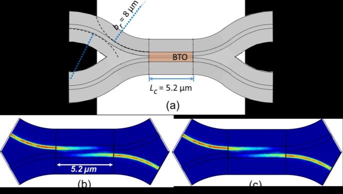
The schematic of the device structure with a new approach to
numerous applications of cutting edge Si photonic technology design using SiO2-BTO-SiO2 hetero-cladding of thickness ‘t’ is
[5-10]. However, large size of photonic devices compared to shown in Fig. 1(a). The coupling gap is taken as 200 nm to
the state-of-the-art electronic counterparts leads to larger ensure it doesn’t violate the minimum experimental limit. In
footprint of Si photonic integrated circuits (PICs). This severely this concept of hetero-cladding, our aim is to gather more light
limits the number of on-chip device integration, hence leads to in the cladding which take part in coupling and reducing the
less functionality of the PICs. To avoid it up to a certain extent, light spreading in other cladding region. At the same time, the
recently, programmable PICs have been developed to facilitate hetero-cladding also includes the technique of releasing more
post-fabrication manipulation and on-demand reconfiguration light from core to cladding without modifying the core structure
of PICs with variety of functionalities [11-13]. These employ unlike the slotted/trenched core structure [32]. The whole
two-dimensional meshes of Mach–Zehnder (MZ) couplers as cladding region of the hetero-cladded coupler is hence devided
their fundamental building elements with a square, triangular, into two parts, named “Region-1” and “Region-2” (indicated in
or hexagonal pattern as their unit cell [11,12,14]. However, figure). Region-1 contributes for light guiding, while region-2
since the size of currently used on-chip conventional MZ is involved in coupling process. Fig. 1(b) shows the schematic
couplers is large (few 10’s of µm), their assembly in a huge of the refractive index profile of the given structure. The idea
number again contributes to extremely large footprint of here is to keep region-1 with a cladding material of high
programmable PICs. To reduce the footprint and making those refractive index contrast (w.r.t core) and to replace region-2
energy efficient, cost effective and multi-functional, it is very with a low refractive index contrast material, to help the mode
essential to design compact MZ couplers. evanescent gather there to enhance the coupling as shown later.
Moreover, the two additional dielectric interfaces formed at the
In search of ultra-compact couplers, researchers have made junction of both the claddings (indicated as dashed orange lines
use of plasmonics, photonic crystals and other techniques [15- in Fig. 1(b)), will prevent spreading of the mode evanescent in
21]. However, most of those follow unconventional design
rules with abundant structural modifications. Realization of
Submitted on October 6, 2021. This work was financially supported Nikhil Ranjan Das is with the Institute of Radio Physics and
by Department of Science and Technology (DST), Govt. of India, Electronics, 92, A.P.C. Road, University of Calcutta, Kolkata 700009,
through INSPIRE Fellowship program under Grant IF150280. India (e-mail: nrd@ieee.org).
Madhusudan Mishra is with the Institute of Radio Physics and
Electronics, 92, A.P.C. Road, University of Calcutta, Kolkata 700009,
India (e-mail: madhusudandbt@gmail.com)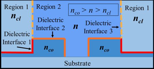
M. Mishra and N. R. Das: “A New Approach of Hetero-Cladding for Design of Compact Si Photonic Directional Coupler” 2
(a)
(c)
(b) (b)
Fig. 1. (a) Schematic of the device structure and (b) refractive index and dielectric interface
asymmetry around the core. Red line is the most reflective and the orange and dashed orange
marked interfaces are less reflective. (c) Schematic circuit lines for biasing-1 and biasing-2.
region-1. As it is shown in Fig. 1(a), BTO is used as cladding is more in the case of hetero-cladding structure, for both even
for region-2, by keeping region-1 as SiO2. This kind of and odd modes as anticipated in section-II. This also happens
cladding design creates a strong reflection of light at the outer for TE modes (Fig. 2 (c) & (d)), but with the mode shapes
walls of the cores (red lines in Fig. 1(b)), whereas a weak pushed more towards the BTO cladding region. This, helps
reflection at the inner wall and top of the cores (solid orange reducing the coupling length (Lc) of TE mode prominently.
lines in Fig. 1(b)). This asymmetry in reflection helps pushing
the mode shape more towards the BTO cladding i.e. to region-
2, without seeking for any modification in the core. Weak
reflection at inner side wall and top of the cores could also help
the device become less sensitive to roughness at the core-
coupling region interface.
The proposed structure can be fabricated using the
procedures indicated in literature [26, 29, 33-35]. For example,
after the growth (/patterning) of the doped Si-core waveguide, Fig. 2. Mode profiles of directional coupler for (a,c) uniform BTO
BTO layer can be deposited around the Si-cores using pulsed cladding, and (b,d) SiO2-BTO-SiO2 hetero-cladding (core width=450 nm).
layer deposition technique [29]. A mask can be used along with .
Results for estimated coupling length for proposed hetero-
a photoresist to etch out the BTO from the sides using
cladding structure as a function of cladding thickness (t) for
inductively coupled plasma (ICP) etching technique leaving
three values of core width (Wc =400, 450 and 500 nm) are
BTO cladding only on the top [35]. It may be mentioned here
shown in Fig. 3. Considering the intermediate Wc, (Fig. 3(b)),
that a slight misalignment of the BTO edge and Si-core edge
Lc is now of only ~ 11 m and 9 m (dashed lines) for TE and
won’t affect the performance reported in this study. The side
TM mode respectively, which saturates at a cladding thickness
cladding now can be filled with growth of SiO2.
of only t ≈ 1300 nm. We have seen from our simulation study
To exploit the electro-optic effect of ferroelectric BTO, three
that, this Lc is ~ 60% smaller than traditional uniform SiO2
independent ITO electrodes could be employed (Fig. 1(a)) in
cladding case (for TE mode) and ~ 40% smaller than uniform
two biasing configurations, say “biasing-1” (to set n to ne) and
BTO cladding case, which occurs at a t which is only < 30 % of
“biasing-2” (to set n to no) (Fig. 1(c)) as reported earlier [28,36].
the t needed in uniform BTO cladding case (where t > 3000
Initially n is taken as no. Also, both the cores are n-doped
nm). As indicated in figure, on changing n from no to ne, Lc for
(~1018) to behave as a part of bottom ITO electrodes.
both TE and TM modes undergo further reduction and finally
converge into an identical value (solid lines in figure). That
III. NUMERICAL RESULTS AND SELECTION OF STRUCTURE
means, for a fixed value of Lc (i.e. of a fabricated structure),
PARAMETERS
both the modes get fully coupled. Moreover, switching n back
This part of study employs FEM based simulator (COMSOL) and forth between ne - no, the power coupling can also be tuned.
to optimize the structure parameters as follows. Comparing Fig. 3(b) with (a) and (c) shows that, Fig. 3(a)
A. Estimation of Core Width and Coupling Length gives larger Lc and Fig. 3(c) shows negligibly small tuning with
Lc values for TE and TM modes. At the same time, Fig. 3(b)
Fig.2 shows a comparison between the mode shapes of the (Wc = 450 nm) shows promising behavior with smaller and
proposed hetero-cladding and the uniform (BTO) cladding identical Lc and equal range of tunability for both n = no and ne,
structure. Comparing Figs. 2(a) and (b) it can be seen that, the as compared to Wc = 400 nm (Fig. 3(a)). Thus, this study found
presence of TM mode evanescent in the central BTO cladding Wc = 450 nm as the optimum waveguide width.
(a) (b) (c)
Fig. 3. Coupling length of
directional coupler with
hetero-cladding for both n =
no (dashed line) and n = ne
(solid line) for wave guide
widths of (a) 400 nm, (b)
450 nm, (c) 500 nm.M. Mishra and N. R. Das: “A New Approach of Hetero-Cladding for Design of Compact Si Photonic Directional Coupler” 3
B. Estimation of Transverse Dimension Simulations show that the power coupling here is 2 % less. It
As shown in Fig.2, light in cladding is mainly present in may be mentioned here that the power coupling can be tuned to
region-2, with its negligible presence in region-1. This greatly some extent by applying a suitable bias as reported earlier [41].
reduces the transverse dimension and power loss of the device.
Absence of mode evanescent beyond few 100’s of nanometers IV. CONCLUSION
from outside wall of the cores allows the side electrodes sit A new approach of hetero-cladding (BTO/SiO2) has been
closer to them without any significant contribution to insertion proposed for realization of compact silicon photonic devices
loss. This leads to the need of less applied voltage. through realization of compact directional coupler. The design
The amount of loss experienced by the structure (with is capable to make the coupler more than 60% smaller
optimized core-to-side electrode gap (del) of 500 nm and compared to traditional uniform SiO2 cladded structure. An
thickness t of 1300 nm) for TE and TM modes are around 0.052 optical design shows high power coupling using the designed
dB and 0.057 dB respectively with n = no, and is 0.035 dB and small coupling length. The concept of hetero-cladding could
0.040 dB for n = ne. The estimated loss for uniform BTO also be used to improve the performance of other type of
cladding case for same structure parameters are around 0.135 couplers, sensors, phase shifter, switches, power splitters etc.
dB and 0.179 dB respectively for TE and TM modes with n =
no, and is 0.138 dB and 0.14 dB with n = ne; thus showing 3-4 ACKNOWLEDGMENT
times improvement in the proposed hetero-cladding structure.
The authors acknowledge Dr. Francesco Morichetti of
Finally, the optimized parameter values are summarized in
Dipartimento di Electtronica, Informazione e Bioingegneria,
Table I. It can be seen that, the values of minimum Lc may be
Politecnico di Milano, Milan, Italy, for his useful advice and
kept ~ 7.1 µm for both TE and TM modes, which may further
support on viability of design from experimental aspects.
reduce if coupling assisted by bending is considered as in an
actual design, discussed in the following sub-section.
TABLE I
OPTIMIZED PARAMETER VALUES OF THE PROPOSED STRUCTURE
Symbol Structure Parameters Optimized Values
t Thickness of cladding 1300 nm
del Core to side electrode Spacing, 500 nm
Wc Width of core 450 nm
Lc Minimum coupling length for TE 11 µm (TE)
and TM mode for n = no 9 µm (TM)
Lc Minimum coupling length for TE 7.18 µm (TE)
and TM mode for n = ne 7.12 µm (TM)
C. Optical Design
Using suitable dimensions as discussed above, the schematic
of optical design and the power coupling plot are shown in
Fig.4. As shown in Fig. 4(a), the structure uses a bending radios
(br) of 8 µm with hetero cladding only in the straight coupling
region. Fig. 4(b) shows the light coupling (seen to be ~97 %
from simulation) with an insertion loss of about 0.14 dB. Thus,
high power coupling can be achieved with this design for
reduced footprint. This Lc is less than the minimum Lc
mentioned in Table I because of the bending arms. Fig. 4 (c)
shows power coupling assuming 50 nm of under-filling at the
bottom of coupling gap (assuming any fabrication constraint).
Fig. 4. (a) Schematic of coupler (b) power coupling for n = ne without
under filling and (c) with 50 nm of under filling.M. Mishra and N. R. Das: “A New Approach of Hetero-Cladding for Design of Compact Si Photonic Directional Coupler” 4
REFERENCES and non-symmetric slotted Si wire waveguides”, J. Opt. 18, pp. 105801,
September 2016. DOI: https://doi.org/10.1088/2040-8978/18/10/105801
[1] J. Xiao, Q. Wei, D. G. Yang, P. Zhang, N. He, G. Q. Zhang, T. L. Ren, X. [21] H. Sattari, A. Y. Takabayashi, Y. Zhang, P. Verheyen, W. Bogaerts, N.
P. Chen “A CMOS-Compatible Hybrid Plasmonic Slot Waveguide With Quack “Compact broadband suspended silicon photonic directional
Enhanced Field Confinement”, IEEE Electron Device Letters 37, pp. 456- coupler”, Opt. Lett. 45, pp. 2997-3000, 2020. DOI:
458, April 2016. DOI: 10.1109/LED.2016.2531990 https://doi.org/10.1364/OL.394470
[2] M. Frounchi, G. N. Tzintzarov, A. Ildefonso, J. D. Cressler, “High [22] F. Eltes, D. Caimi, F. Fallegger, M. Sousa, E. O’Connor, M. D. Rossell,
Responsivity Ge Phototransistor in Commercial CMOS Si-Photonics B. Offrein, J. Fompeyrine, S. Abel, “Low-loss BaTiO3-Si waveguides for
Platform for Monolithic Optoelectronic Receivers”, IEEE Electron nonlinear integrated photonics”, ACS Photonics 3(9), pp. 1698-1703,
Device Letters 42, pp. 196-199, Feb. 2021. DOI: August 2016. DOI: https://doi.org/10.1021/acsphotonics.6b00350
10.1109/LED.2020.3042941 [23] K. J. Kormondy, Y. Popoff, M. Sousa, F. Eltes, D. Caimi, M. D Rossell,
[3] R. Won, “Integrating silicon photonics”, Nature Photonics 4, pp. 498– M. Fiebig, P. Hoffmann, C. Marchiori, M. Reinke, M. Trassin, A. A
499, August 2010. DOI: https://doi.org/10.1038/nphoton.2010.189 Demkov, J. Fompeyrine, S. Abel, “Microstructure and ferroelectricity of
[4] Y. Li, L. Yang, H. Zou, H. S. Zhang, X. H. Ma, Y. Hao, “Substrate BaTiO3 thin films on Si for integrated photonics,” Nanotechnology 28,
Integrated Waveguide Structural Transmission Line and Filter on Silicon 075706, January 2017. DOI: https://doi.org/10.1088/1361-6528/aa53c2
Carbide Substrate”, IEEE Electron Device Letters 38, pp. 1290-1293, [24] S. Abel, T. Stoferle, C. Marchiori, D. Caimi, L. Czornomaz, M.
Sept. 2017. DOI: 10.1109/LED.2017.2734947 Stuckelberger, M. Sousa, B. J. Offrein, J. Fompeyrine, “A hybrid barium
[5] D. Thomson, A. Zilkie, J. E. Bowers, T. Komljenovic, G. T. Reed1, L. titanate–silicon photonics platform for ultraefficient electro-optic tuning,”
Vivien, D. M. Morini, E. Cassan, L. Virot, J. M. Fédéli, J. M. Hartmann, J. Lightwave Technol. 34, 1688–1693, December 2015. DOI:
J. H. Schmid, D. X. Xu, F. Boeuf, P. O'Brien, G. Z Mashanovich, M. 10.1109/JLT.2015.2510282
Nedeljkovic “Roadmap on silicon photonics”, Journal of Optics 18, [25] C. Xiong, W. H. P. Pernic, J. H. Ngai, J. W. Reiner, D. Kumah, F. J.
pp.073003, June 2016, DOI: https://doi.org/10.1088/2040- Walker, C. H. Ahn, H. X. Tang, “Active Silicon Integrated
8978/18/7/073003 Nanophotonics: Ferroelectric BaTiO3 Devices”, Nano Lett. 1, pp. 1419-
[6] X. Wang, J. Liu, “Emerging technologies in Si active photonics”, Journal 1425, January 2014. DOI: https://doi.org/10.1021/nl404513p
of Semiconductors 39, June 2018. DOI:https://doi.org/10.1088/1674- [26] E. L. Lin, A. B. Posadas, L. Zheng, J. E. Ortmann, S. Abel , J. Fompeyrine,
4926/39/6/061001 K. Lai , A. A. Demkov , J. G. Ekerdt, “Atomic layer deposition of epitaxial
[7] F. Giuseppe, D. Corte, S. Rao, “Use of Amorphous Silicon for Active ferroelectric barium titanate on Si(001) for electronic and photonic
Photonic Devices”, IEEE Transactions on Electron Devices 60, pp.1495- applications”, J. Appl. Phys. 126, pp. 064101(1-9), August 2019. DOI:
1505, May 2013. DOI: 10.1109/TED.2013.2249069 https://doi.org/10.1063/1.5087571
[8] M. Chacinski, U. Westergren, B. Stoltz, L. Thylen , “Monolithically [27] M. J. Dicken, L. A. Sweatlock, D. Pacifici, H. J Lezec, K. Bhattacharya,
Integrated DFB-EA for 100 Gb/s Ethernet”, IEEE Electron Device Letters H. A Atwater, “Electrooptic modulation in thin film barium titanate
29, pp. 1312-1314, Dec. 2008. DOI: 10.1109/LED.2008.2007222 plasmonic interferometers,” Nano Lett. 8, 4048–4052 November 2008.
[9] A. Noriki, K. Lee, J. Bea, T. Fukushima, T. Tanaka, M. Koyanagi, DOI: 10.1021/nl802981q
“Through-Silicon Photonic Via and Unidirectional Coupler for High- [28] M. Mishra, N. R. Das, A. Melloni, F. Morichetti, “Modelling domain
Speed Data Transmission in Optoelectronic Three-Dimensional LSI”, switching of ferroelectric BaTiO3 integrated in silicon photonic
IEEE Electron Device Letters 33, pp. 221-223, Feb. 2012. DOI: waveguides,” Opt. Commun. 448, 19–25, October 2019. DOI:
10.1109/LED.2011.2174608 https://doi.org/10.1016/j.optcom.2019.05.001
[10] Z. Zhou, R. Chen, X. Li, T. Li, “Development trends in silicon photonics [29] I. M. Albo, S. Varotto, M. Asa, C. Rinaldi, M. Cantoni, R. Bertacco, F.
for data centers”, Optical Fiber Technology 44, pp. 13-23, August 2018. Morichetti, “Non-volatile switching of polycrystalline barium titanate
DOI: https://doi.org/10.1016/j.yofte.2018.03.009 films integrated in silicon photonic waveguides,” in Advanced Photonics
[11] W. Bogaerts, D. Pérez, J. Capmany, D. A. B. Miller, J. Poon, D. Englund, 2018 (BGPP, IPR, NP, NOMA, Sensors, Networks, SPPCom, SOF), OSA
F. Morichetti, A. Melloni, “Programmable photonic circuits”, Nature 586, Technical Digest (online) (Optical Society of America, 2018), paper
pp. 207–216, October 2020. DOI: https://doi.org/10.1038/s41586-020- ITu4I.2. DOI: https://doi.org/10.1364/IPRSN.2018.ITu4I.2
2764-0 [30] T. Mikolajick, “The Past, the Present, and the Future of Ferroelectric
[12] D.P. López, “Principles, fundamentals, and applications of programmable Memories”, IEEE Transactions on Electron Devices 67, NO. 4, pp.1434-
integrated photonics”, Adv. in Opt. and Photonics 12, pp. 709-785, 2020. 1443, March 2020. DOI: 10.1109/TED.2020.2976148
DOI: https://doi.org/10.1364/AOP.387155 [31] R. P. Shi, X. D. Huang, J. K. O. Sin, P. T. Lai “Y-Doped BaTiO3 as a
[13] H. Zhou, Y. Zhao, X. Wang, D. Gao, J. Dong, X. Zhang, “Self- Charge-Trapping Layer for Nonvolatile Memory Applications”, IEEE
Configuring and Reconfigurable Silicon Photonic Signal Processor”, Electron Device Letters 37, pp. 1555-1558, Dec. 2016. DOI:
ACS Photonics 7, pp. 792-799, February 2020. DOI: 10.1109/LED.2016.2615063
https://doi.org/10.1021/acsphotonics.9b01673 [32] M. Mishra and N. R. Das, “Trenched Core Waveguide Structure for
[14] D. Perez and I. Gasulla, “Toward programmable microwave photonics Photonic Integrated Circuit”, in “Computers and Devices for
processors,” J. Lightwave Technology 36, 519–532, 2018. DOI: Communication", N. R. Das and Santu Sarkar (Eds.), Lecture Notes in
10.1109/JLT.2017.2778741 Networks and Systems, Springer Nature Singapore Pte. Ltd. 147, 321
[15] C.-H. Du and Y. P. Chiou, “Vertical Directional Couplers with Ultra- February 2021. DOI: 10.1007/978-981-15-8366-7_46
Short Coupling Length Based on Hybrid Plasmonic Waveguides”, Journal [33] Y.-J. Seo and W.-S. Lee, “Chemical Mechanical Polishing Characteristics
of Lightwave Technology 32, pp. 2065-2071, June 2014. DOI: of Barium Titanate Thin Films Using Mixed Abrasive Slurry”, Journal of
10.1109/JLT.2014.2318182 the Korean Physical Society 48, pp. 1651-1656, 2006.
[16] L. Ye, Y. Zheng, J. Wang, H. Liao, R. Huang, “Miniature CMOS Stacked https://www.jkps.or.kr/journal/view.html?uid=7625&vmd=Full
Spiral-Coupled Directional Coupler With −67-dB Isolation and − 0.8-dB [34] Y. Li, C. Wang, Z. Yao, H. K. Kim, N. Y. Kim, “Comparative analysis
Insertion Loss”, IEEE Electron Device Letters 33, pp. 919-921, July 2012. of barium titanate thin films dry etching using inductively coupled
DOI: 10.1109/LED.2012.2196749 plasmas by different fluorine-based mixture gas”, Nanoscale Research
[17] C. E. Garcia-Ortiz, V. Coello, E. Pisano, Y. Chen, S. I. Bozhevolnyi , Letters 9.1, September 2014. DOI: https://doi.org/10.1186/1556-276X-9-
“Plasmonic directional couplers using channel waveguides in random 530
arrays of metal nanoparticles”, Optics Express 27, pp. 22753-22763, [35] C. Wang, H.K. Sung, N.Y. Kim, “Aerosol deposition-based
2019. DOI: https://doi.org/10.1364/OE.27.022753 micropatterning of barium titanate via sulphur hexafluoride inductively
[18] N. Janrao, and V. Janyani, “Ultra compact slow light photonic crystal coupled plasma etching”, Vacuum 114, pp. 49-53, April 2015. DOI:
directional coupler design with elliptical rods”, Optik 124, pp. 3120– 3124 https://doi.org/10.1016/j.vacuum.2014.12.028
2013. DOI: https://doi.org/10.1016/j.ijleo.2012.09.039 [36] M. Mishra, N. R. Das and F. Morichetti, “Waveguide design optimization
[19] H. Xie, J. Zheng, P. Xu, J. Yao, J. Whitehead, A. Majumdar , “Ultra- for compact silicon photonic ferroelectric phase shifters”, Applied Optics
Compact Subwavelength-Grating-Assisted Polarization-Independent 59, pp. 4385-4391 May 2020. DOI: https://doi.org/10.1364/AO.390273
Directional Coupler”, IEEE Photonics Technology Letters 31, pp. 1538-
1541, August 2019. DOI: 10.1109/LPT.2019.2937890
[20] R. Haldar, V. Mishra, A. Dutt, S. K Varshney, “On-chip broadband ultra-
compact optical couplers and polarization splitters based on off-centeredYou can also read


