A novel true random number generator based on a stochastic diffusive memristor - Nature
←
→
Page content transcription
If your browser does not render page correctly, please read the page content below
ARTICLE
DOI: 10.1038/s41467-017-00869-x                OPEN

A novel true random number generator based on a
stochastic diffusive memristor
Hao Jiang1, Daniel Belkin1,2, Sergey E. Savel’ev 3, Siyan Lin1, Zhongrui Wang1, Yunning Li1, Saumil Joshi1,
Rivu Midya1, Can Li 1, Mingyi Rao1, Mark Barnell4, Qing Wu4, J. Joshua Yang 1 & Qiangfei Xia1

The intrinsic variability of switching behavior in memristors has been a major obstacle to their
adoption as the next generation of universal memory. On the other hand, this natural sto-
chasticity can be valuable for hardware security applications. Here we propose and
demonstrate a novel true random number generator utilizing the stochastic delay time of
threshold switching in a Ag:SiO2 diffusive memristor, which exhibits evident advantages in
scalability, circuit complexity, and power consumption. The random bits generated by the
diffusive memristor true random number generator pass all 15 NIST randomness tests
without any post-processing, a first for memristive-switching true random number gen-
erators. Based on nanoparticle dynamic simulation and analytical estimates, we attribute the
stochasticity in delay time to the probabilistic process by which Ag particles detach from a Ag
reservoir. This work paves the way for memristors in hardware security applications for the
era of the Internet of Things.

1 Department of Electrical and Computer Engineering, University of Massachusetts, Amherst, MA 01003, USA. 2 Swarthmore College, Swarthmore, PA

19081, USA. 3 Department of Physics, Loughborough University, Loughborough LE11 3TU, UK. 4 Air Force Research Lab, Information Directorate, Rome, NY
13441, USA. Hao Jiang, Daniel Belkin and Sergey E. Savel’ev contributed equally to this work. Correspondence and requests for materials should be addressed
to J.J.Y. (email: jjyang@umass.edu) or to Q.X. (email: qxia@umass.edu)

NATURE COMMUNICATIONS | 8: 882       | DOI: 10.1038/s41467-017-00869-x | www.nature.com/naturecommunications                                             1
ARTICLE                                                                                                        NATURE COMMUNICATIONS | DOI: 10.1038/s41467-017-00869-x

T
       he internet of things (IoT) is a network of devices, sensors,                            dependent on the applied voltages29. Balatti et al. demonstrated a
       and other items of various functionalities that interact and                             TRNG using cycle-to-cycle and device-to-device voltage varia-
       exchange data electronically1. Because of the explosive                                  tions from Cu/AlOx and Ti/HfOx based memristors, respec-
growth in the number of IoT objects (estimated to be 50 billion by                              tively30, 31. Besides the need for complicated probability tracking
20202) and overwhelming reliance on cyberspace, the existing                                    and careful tuning of the applied voltage/current, a pair of SET
hardware infrastructure is increasingly vulnerable to a wide range                              and RESET pulses were required to generate each random bit
of security threats3. When software-based data securing methods                                 since those memristive devices are non-volatile. More impor-
are no longer sufficient because they are easily attacked, hardware                              tantly, none of the aforementioned memristor based TRNGs
security systems become critical. A true random number gen-                                     passed all the 15 NIST Special Publication 800-22 randomness
erator (TRNG) is a hardware component that generates a string                                   tests32 even with post-processing of data, leaving the claimed true
of random bits, which can be used as a cryptographic key. It relies                             nature of the randomness debatable. Most recently, Wei et al.
on intrinsic stochasticity in physical variables as a source of                                 demonstrated a TRNG using randomness from small read-
randomness. For example, thermal noise is often exploited by                                    current fluctuation at certain resistance states in TaOx-based
TRNGs via oscillator jitter4, resistor-amplifier-Analog/Digital                                  devices. Sophisticated algorithms and circuits were needed to
converter chains5, or metastable elements with capacitive feed-                                 ensure the quality of generated binary bits before they could pass
back6. Other approaches include using telegraph noise7, current                                 the NIST tests33.
fluctuation in oxide after soft breakdown8, or time-dependent                                       Here, we propose and demonstrate a novel TRNG based on a
oxide breakdown process9. However, all prior TRNGs have suf-                                    diffusive memristor, a newly developed volatile device that relies
fered from drawbacks in scalability, circuit complexity, or relied                              on the diffusion dynamics of metal atoms in the memristive
on post-processing such as a “Von Neumann corrector” to                                         layer34, 35. The device switches to a low-resistance state under a
remove bias from the generated bit sequences4–13.                                               voltage pulse after a random delay time, and relaxes back to the
   Memristors14–16, or resistive switching devices, have been                                   high-resistance state spontaneously upon removal of the applied
proposed and demonstrated for a broad spectrum of                                               electrical bias. We use the intrinsic stochasticity of the delay time
applications16–19 because of their attractive properties, such as                               as the source of randomness to build a TRNG unit that consists of
low power consumption20, fast switching speed21, high endur-                                    only a diffusive memristor, a comparator, an AND-gate, and a
ance22, excellent scalability23, and CMOS-compatibility24. The                                  counter. Compared with previous TRNGs based on non-volatile
intrinsic variation in switching parameters is a major challenge                                memristors30, 31, the self-OFF-switching behavior in the diffusive
for some applications such as non-volatile memory25. However,                                   memristor greatly reduces the energy consumption since no
this random behavior can be helpful in stochastic computing and                                 RESET process is required. Our TRNG also has evident advan-
hardware security applications26–28. For example, Huang et al.                                  tages in circuit complexity because the randomness is generated
proposed a TRNG based on random telegraph noise (RTN) from                                      and harvested directly using simple elements. The diffusive
the low resistance state of a W/TiN/TiON/SiO2/Si memristor.                                     memristor TRNG can easily be incorporated into memory sub-
The resulting circuit, however, proved difficult to activate and                                 systems, greatly increasing the security, and the area efficiency33.
control because the probabilities of “0” and “1” were heavily                                   More importantly, the bits generated by our diffusive memristor

                                          a                                                     b
                                                                            20 nm Pt/30 nm Au                  10–7
                                                                                 5 nm Ag
                                                                                                                             Vhold
                                                                              10 nm Ag:SiO2
                                                                                                Current (A)

                                                                                15 nm Pt                       10–9

                                                                                                              10–11

                                                                                                                                                  Vthreshold
                                                                                                              10–13
                                                                                                                  0.0        0.2         0.4     0.6       0.8
                                                                                                                                     Voltage (V)

                            c                                                                   d
                                          0.6
                                                    Vin          Delay time
                                                                                                              40    0.9 V
                                                                                      Vin
                                                          Diffusive
                                                                                      Vout                            0.8 V
                                                          memristor
                            Voltage (V)

                                          0.4                                                                 30
                                                                                                Counts (#)

                                                                                                                        0.7 V        0.5 V
                                                                                                                                                 0.4 V
                                                          Series                                              20            0.6 V
                                          0.2             resistor     Relaxation time
                                                                                                              10

                                          0.0                                                                  0
                                                0           2        4            6                             0      50   100 150 200 250 300 350
                                                                 Time (ms)                                                    Delay time (μs)

Fig. 1 Stochastic threshold switching behavior in a Ag:SiO2 based diffusive memristor. a Optical microscopic image of the 5 × 5 µm2 Ag:SiO2 cross-point
device. Scale bar, 50 µm. Inset shows geometry of the Ag:SiO2 diffusive memristor. Note that a 5 nm Ag layer is inserted between switching layer and top
electrode to provide enough Ag supply. b 50 Consecutive DC switching cycles of the diffusive memristor connected to a 4.7 MΩ series resistor. c Typical
pulse switching behavior of the diffusive memristor. Under a voltage pulse (300 µs in this case), some delay time is needed before the device abruptly
turns ON. Inset shows the circuit for the measurements with a 120 kΩ resistor connected in series to the memristor. d Distribution of delay time for
different input pulse amplitude (0.4 to 0.9 V at 50 Hz). A higher voltage leads to a shorter average delay time with a narrower distribution

2                                                                    NATURE COMMUNICATIONS | 8: 882                 | DOI: 10.1038/s41467-017-00869-x | www.nature.com/naturecommunications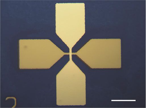
NATURE COMMUNICATIONS | DOI: 10.1038/s41467-017-00869-x                                                                                                   ARTICLE

TRNG pass all 15 NIST Special Publication 800-22 randomness                                 SiO2 layer deposited on a thin SiNx membrane fabricated in the
tests without any post-processing. Utilizing nanoparticle dynamic                           same batch, dense Ag nanoclusters (mostly 2 to 5 nm in diameter
simulations and simple analytical estimates, we reveal for the first                         with a few outliers of 10 nm) were uniformly dispersed in the
time that the stochasticity in delay time originates from the sto-                          SiO2 matrix (Supplementary Fig. 1b).
chastic process by which Ag particles detach from a Ag reservoir                              The Ag:SiO2 device did not require electroforming and
before their transportation to form the conduction channel(s)                               exhibited reliable threshold under quasi-DC sweeps with a
within SiO2 matrix. The new mechanism based on ionic/atomic                                 > 105 ON/OFF window, a sub-100 nA operation current and an
motion indicates that our TRNG may be less vulnerable to                                    extremely low (< pA) leakage current at OFF state (Fig. 1b). The
environmental variations such as radiation relative to other                                device abruptly reached a low resistance state at a threshold
electron-based TRNGs36.                                                                     voltage of around 0.5 V (ON-switching), followed by a sponta-
                                                                                            neous relaxation back to the high-resistance state when the
                                                                                            voltage swept back to below 0.3 V (self-OFF-switching), confirm-
Results                                                                                     ing the volatility of the device. Multiple switching sweeps of the
Stochastic volatile switching behavior of a Ag:SiO2 diffusive                               device also showed evident cycle-to-cycle variations in threshold
memristor. The optical image and geometry of a Ag:SiO2 based 5                              voltage, verifying the stochastic nature of the switching behavior.
µm × 5 µm cross-point diffusive memristor used in this work is                              A series resistor was found effective in limiting the ON-state
schematically shown in Fig. 1a. The device has a Pt/Ag/Ag:SiO2/                             current and tuning the ON/OFF window (Supplementary Fig. 2).
Pt stack with another 30 nm thick Au on the top electrode for                                 Stochastic delay time was observed before the sudden increase
better contact with measurement probes (see Methods for device                              in device conductance during ON-switching under an electric
fabrication details). Unlike in diffusive memristors used for other                         pulse (Fig. 1c). A 300 µs pulse of 0.5 V (Vin) was applied to the
applications34, an extra Ag layer (5 nm) was inserted between the                           device, and the voltage across the series resistor (Vout) was
switching layer and the top electrode as a reservoir of Ag atoms to                         monitored by an oscilloscope. Under this specific applied Vin, a
avoid any Ag depletion during switching. After fabrication, the                             finite delay time (incubation period, ~ 130 µs) was required before
Ag doping ratio in the Ag:SiO2 switching layer was determined to                            Vout abruptly increased, indicating ON-switching of the device.
be around 17% (atomic ratio) by X-ray photoelectron spectro-                                When the applied voltage was removed, the device relaxed to the
scopy (XPS; Supplementary Fig. 1a). According to bright-field                                OFF state within 100 μs, as read by a subsequent 50 mV pulse.
transmission electron microscopy (TEM) analysis of a 10 nm Ag:                              Figure 1d shows the statistics of the measured delay time under

                                                a
                                                      Pulse
                                                                        1
                                                                                      Clock
                                                                                               4
                                                                            Vref

                                                                                              AND       Counter
                                                                                CMP
                                                                 2                                  5                   6
                                                                                       3

                       b
                                 1                    V1                    2          V2                           3                    V3
                                                                                       Input pulse V1                                    Input pulse V1
                                                                                       Vref                                              V2
                       Voltage

                                                              Voltage

                                                                                                          Voltage

                                        Time                                          Time                                        Time
                                 4                                          5          V5                           6   Bit            Bit      Bit
                                                      V4
                                                                                       Input pulse V1               pre-status     flipping post-status
                                                                                       V2
                                                              Voltage

                                                                                                          Voltage

                                                                                                                                              “1”
                       Voltage

                                                                                       V3                                   “0”

                                        Time                                          Time                                        Time

Fig. 2 Working principle of a diffusive memristor based true random number generator (TRNG). a Circuit diagram of a TRNG with a diffusive memristor,
a comparator (CMP), an AND gate, and a counter. b Schematic pulse waveforms at each stage of the circuit (as labeled in a), illustrating the working
principle of our diffusive memristor TRNG. The stochastic delay time of the diffusive memristor leads to variations of the pulse width (shown in 3) and then
random numbers of clock pulses that are sent to the counter (shown in 5). The bit status (counter output) before, during and after flipping is labeled in red
in 6. The bit flipping is triggered by the rising edge of clock signal and hence the bit flipping frequency is half of the clock frequency. The counter output is
random due to the random times of bit flipping, as determined by the random numbers of clock pulses sent to the counter (V5)

NATURE COMMUNICATIONS | 8: 882        | DOI: 10.1038/s41467-017-00869-x | www.nature.com/naturecommunications                                                   3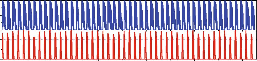
ARTICLE NATURE COMMUNICATIONS | DOI: 10.1038/s41467-017-00869-x
different voltages (from 0.4 to 0.9 V). A higher voltage leads to a concept unit with a diffusive memristor, a comparator, an AND-
shorter average delay time with a narrower distribution. The gate, and a counter. Figure 2b illustrates the operating principle of
stochastic delay time can be linked to the process of forming the our TRNG with waveforms corresponding to each stage of the
Ag conduction channel(s), as will be discussed later in detail. circuit as labeled in Fig. 2a. A voltage pulse (V1) of fixed width is
Moreover, the delay time is also dependent on pulse frequency. applied across a diffusive memristor and a series resistor (Panel 1).
As shown in Supplementary Fig. 3, a higher frequency leads to Under the applied voltage, the diffusive memristor is turned ON
shorter delay times even with the same voltage amplitude and and hence the output voltage (V2) across the series resistor sud-
pulse width (0.5 V, 300 µs), which may be related to an increase of denly increases after a stochastic delay time (Panel 2). When V2 is
temperature of the device at higher pulse frequencies. Other higher than a reference voltage to the comparator (Vref), the
factors including the speed of capacitor charging could also play comparator output voltage (V3) goes to a logic high level (Panel 3),
a role. and V2 and V3 fall back to zero when the single input pulse (V1)
ends. Since the delay time of the diffusive memristor is random,
the comparator output voltage pulse V3 has a random width. V3
TRNG based on a diffusive memristor. The stochastic delay and a high frequency clock signal (V4) are sent to an AND gate,
time of the Ag:SiO2-based diffusive memristor during ON- whose output voltage pulses (V5 in Panel 5) are sent to a counter.
switching was utilized as the source of randomness for our Panel 6 shows the binary bit (counter output, in red) stays at its
TRNG. Figure 2a shows the circuit diagram of the proof-of- pre-status (“0”) before the device is turned ON, flips rapidly
(triggered by clock signals) until the single input pulse (V1) ends
and then stays at its post-status (“1”). The bit flipping in the
a b counter is triggered by the rising edge of the clock signal, and
Bit
10 hence has a frequency half of the clock frequency. The bit on
Delay Bit
Bit pre-status time flipping post-status
0.4 which the counter stops is random, because the stochastic delay
Voltage (V)
Voltage (V)
Input
Counter output “1”
5
time of the diffusive memristor leads to random pulse width from
0.2
Counter
the comparator (V3) and thus a random number of clock pulses
working that are sent to the counter. The random bit generation rate can
“0”
0.0 0 be increased using a multi-bit counter, with which one stochastic
0.0 0.2 0.4 0.6 volatile switching event can produce more than one binary bit
Time (ms) (Supplementary Fig. 4).
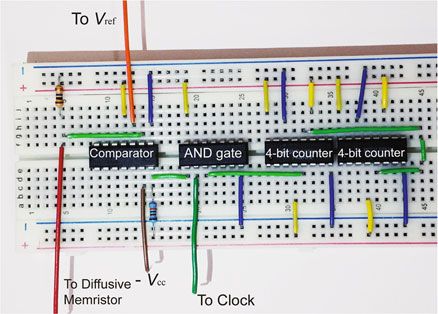
c The diffusive memristor TRNG was experimentally imple-
10 mented by a simple circuit built on a breadboard (Fig. 3a). To
“1” “0” “0” “1” “0” demonstrate the operation of our diffusive memristor TRNG, the
0.4
lowest order bit of the counter output was monitored by an
Voltage (V)
Input
Voltage (V)
5 oscilloscope during operation (Fig. 3b). We used a pulse train of
0.2
Counter constant amplitude (V1 = 0.4 V) with pulse width of 300 and 700
output
µs spacing (i.e., 1 kHz frequency). As shown in Fig. 3b, the bit was
0.0 0 initially at a low logic level (“0”). After the delay time (once the
diffusive memristor switched to ON state) the counter started
0 2 4
TIme (ms)
receiving clock signals (at 4 MHz) and the bit flipped rapidly
between low and high level (“0” and “1”). At the end of the input
Fig. 3 Experimental demonstration of a diffusive memristor true random pulse (V1), the counter stopped counting and kept its last state “1”
number generator. a Photo of our simple circuit built on a breadboard. until receiving the next counting signal. This “1” was the output
b Monitored one counter output in response to input voltage pulse (1 kHz) bit read by the microcontroller. Due to the stochastic nature of
applied on our diffusive memristor. c Monitored one random binary output the delay time for each cycle, the counter output after each
flipping from “1” → “0” → “0” → “1” → “0” over continuous switching cycles pulse was totally unpredictable and flipped randomly between “0”
Table 1 Randomness test (NIST 800-22 test suite) results for a diffusive memristor true random number generator
P-value Pass rate min. pass rate Success/failure
1. Approximate entropy 0.00983 75/76 72/76 Success
2. Block frequency 0.768138 75/76 72/76 Success
3. Cumulative sums 0.046525, 0.426525 73/76, 74/76 72/76 Success
4. FFT 0.739918 75/76 72/76 Success
5. Frequency 0.477737 74/76 72/76 Success
6. Linear complexity 0.350485 76/76 72/76 Success
7. Longest run 0.042413 76/76 72/76 Success
8. Non overlapping template - 11052/11248 10656/11248 Success
9. Overlapping template 0.592591 75/76 72/76 Success
10. Random excursions - 360/368 344/368 Success
11. Random excursions variant - 818/828 774/828 Success
12. Rank 0.094936 76/76 72/76 Success
13. Runs 0.042413 75/76 72/76 Success
14. Serial 0.739918, 0.795464 76/76, 76/76 72/76 Success
15. Universal 0.000954 76/76 72/76 Success
Total 76M binary bits are collected from our diffusive memristor TRNG and then divided into 76 sequences (1M bits each). Tests are considered passing if P-value (except non-overlapping-template and
random excursions variant) is > 0.0001 and the pass rate exceeds the minimum pass rate for each test. Our diffusive memristor TRNG passed all the 15 tests without any post-processing, confirming its
reliable performance
4 NATURE COMMUNICATIONS | 8: 882 | DOI: 10.1038/s41467-017-00869-x | www.nature.com/naturecommunications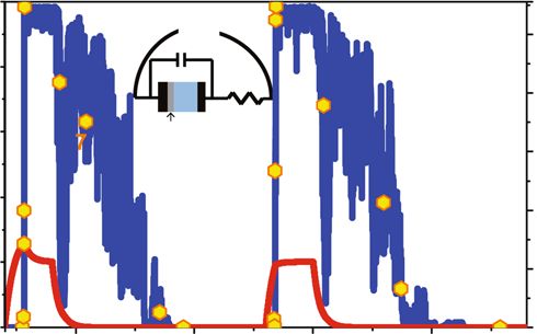
NATURE COMMUNICATIONS | DOI: 10.1038/s41467-017-00869-x ARTICLE
a c 1
d
1.0 1 14
G/Gmax
G/Gmax
5
G/Gmax
V(t) 13
C
5
0.5
V/Vth
6 Rex
Oxide
Pt Pt 15
0.0 0.6
b 1
0.6 7 Ag
3
V/Vth
12
0.4 0.4 4 16
0 2
3
0 4000 8000 12,000 16,000 20,000 0.2 0.2 17 1
κt 2 8 9 11 18
0 0 1 10 0
0
10
20
30
40
5
18,600 18,800 19,000 19,200
κt κt
e
50
1 2 3 4 5 6 7 8 9
Ag-nanoparticles probability
0.5
distribution
50
10 11 12 13 14 15 16 17 18
0.5
–1 –0.5 0 0.5 –0.5 0 0.5 –0.5 0 0.5 –0.5 0 0.5 –0.5 0 0.5 –0.5 0 0.5 –0.5 0 0.5 –0.5 0 0.5 –0.5 0 0.5 1.0
x/L x/L x/L x/L x/L x/L x/L x/L
f g h i
30 30
Transportation 200
t0 from fitting (ms)
20 0.4 V 0.7 V
Counts (#) 150
Counts (#)
20
U/kBT0
15 100
10
10
Detaching 50
0 0 0 0
–1.0 –0.5 0.0 0.5 1.0 200 250 300 350 400 40 50 60 70 80 90 100 0.4 0.5 0.6 0.7 0.8 0.9
x/L Delay time (μs) Delay time (μs) Voltage (V)
Fig. 4 Physical origin of stochastic delay time clarified by nanoparticle dynamics simulations. a The switching of the simulated memristor conductance
when 48 rectangular voltage pulses are applied, with conductance normalized by the maximum memristor conductance, and b the variation of voltage
across the memristor, normalized by the threshold voltage Vth. c The switching to the low resistive state at time measured from the beginning of the
corresponding pulses. The randomness of the resistive switching is clearly seen. d The two chosen resistive switches with different delay time and
e corresponding particle probability distributions (1–18) marked on d by yellow points. Inset in d shows the circuit model used during the simulation. The
memristor is connected with a parallel capacitor and a series resistor. f Potential normalized by thermal fluctuations across the sample used here. The
delay time is composed of charging time of capacitor, time of Ag particles detach from Ag reservoir and the Ag transportation time until the formation of
conduction channel(s), while the stochasticity is mainly attributed to the stochastic detaching process. For simulations in a–e, we used the following
voltage pulse parameters: voltage pulse duration κtp = 80 (allowing enough time to switch to low resistive state for every pulse), inter-pulse interval
κΔt = 360 (allowing enough times to relax) and voltage amplitude Vam/Vth = 1.6, potential versus temperature as in f (all times measured in unit of thermal
relaxation time 1/κ). The experimental delay time distributions under (g) 0.4 V and (h) 0.7 V fitted by eq. 2. i The fitting curve of t0 vs. pulse amplitudes
according to eq. (3). The fitted probability distributions appear to be consistent with experimental results, confirming the feasibility of our proposed
mechanism
and “1”. Figure 3c shows the monitored binary bits randomly Physical origin of stochastic switching delay time in Ag:SiO2
flipped from “1” → “0” → “0” → “1” → “0” during four contin- diffusive memristors. To better understand the physical origin of
uous ON-switching cycles. the delay time and confirm its stochastic nature, we performed
To assess the performance of our diffusive memristor TRNG, nanoparticle dynamical simulations utilizing a generalized model
we carried out randomness testing for 76 million binary bits using that links electrical, nano-mechanical and thermal degrees of
the standard statistical testing package developed by the National freedom (see Methods). Unlike previous studies that mainly
Institute of Standards and Technology (NIST 800-22 test suite)32. focused on response to a single pulse34, 35, multi-switching-cycles
We used a microcontroller’s built-in 16-bit counter with under a train of pulses were simulated. In addition to the equa-
11.0592 MHz crystal oscillation frequency as the clock signal tions for heat and Ag-nanoparticle dynamics used in previous
and the 6 lowest-order bits were collected. Each input pulse will model34, 35, we also took into account both external and intrinsic
give us 6 random binary bits, for a total bit generation rate of memristor capacitances37, 38 in order to better resemble the real
6 kbs−1. According to the test protocol, 76 million bits were conditions during experiments (see also Methods section).
collected (see Methods for more details) and divided into Figures 4a, b show the simulation results of 48 volatile switching
76 sequences (1 M bits each) for the NIST tests, which returned cycles: switching of conductance G (normalized by its maximum
two statistics, P-value (except non-overlapping-template and value) is shown in Fig. 4a, while the voltage across the memristor
random excursions variant) and pass rate. The bits are considered is shown in Fig. 4b. With the same input pulses, random delay
random and successfully pass the test only if the P-value is greater time during ON-switching was clearly observed in Fig. 4c (with
than 0.0001 and the pass rate exceeds the minimum value defined time counted from the moment when the corresponding voltage
by NIST. As shown in Table 1, our diffusive memristor TRNG pulse was applied). The delay time statistics from simulations also
passed all 15 NIST tests without any post-processing. confirm a shorter delay time and a narrower distribution with
NATURE COMMUNICATIONS | 8: 882 | DOI: 10.1038/s41467-017-00869-x | www.nature.com/naturecommunications 5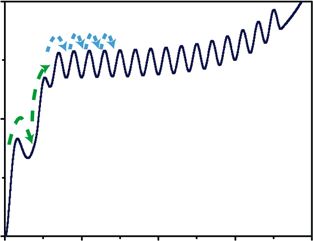
ARTICLE                                                                       NATURE COMMUNICATIONS | DOI: 10.1038/s41467-017-00869-x

increasing applied voltage amplitudes (Supplementary Fig. 5a),           by solving the Fokker-Plank equation with parabolic well and
similar to experimental results shown in Fig. 1d. Moreover, the          delta-function (for classical) or ground state (for quantum) initial
obtained distribution statistics of simulated and measured delay         distribution of Ag-nanoparticles in the potential minima
times are very similar.                                                  (Supplementary Note 1, Supplementary Figs. 6 and 7). In classical
    Evolution of Ag nanoparticle density distribution during two         limit the delay time distribution has the form:
typical switching cycles (with G(t) presented in Fig. 4d) with quite
                                                                                                     Ce1e2kte
                                                                                                                 A

different delay times was shown in Fig. 4e (panels 1–18) step by                                                                 1
                                                                                            Pðte Þ ¼ pffiffiffiffiffiffiffiffiffiffiffiffiffiffiffiffiffi e2kte 1                   ð1Þ
step. A simple circuit model used during the simulation is                                            1e     2kt   e

schematically shown as an inset in Fig. 4d, which consists of a
memristor, a parallel capacitor and a series resistor. The capacitor     Where A and k are fitting parameters related to potential
represents capacitances from the device itself and also from the         curvature and depth of the well, and C is a normalization
external circuits during electrical measurements such as cables          constant. Adding the deterministic RC effect (Supplementary
and breadboards. As mentioned above, a series resistor is used to        Note 2), one can easily get the distribution of stochastic delay
limit the operation current. When a voltage is applied, the voltage      time (t):
across memristor gradually increases (Fig. 4d, the red curve). As
                                                                                                 Ce 1e2kðtt0 Þ                      1
                                                                                                            A
soon as the voltage exceeds the threshold Vth, Ag nano-particles                                                                                   ð2Þ
                                                                                        Pðt Þ ¼ pffiffiffiffiffiffiffiffiffiffiffiffiffiffiffiffiffiffiffiffiffiffiffiffi e2kðtt0 Þ 1
can randomly detach from the Ag-electrode and form a large                                        1e2kðtt0 Þ
cluster nearby (Fig. 4e, panel 1). Some particles escape from the
cluster and start to diffuse towards the right electrode (Pt) driven
by the electric field (Fig. 4e, panel 2) and the memristor resistance                                          Vtr
                                                                                               t0 ¼ τ0 ln 1       þ t1                           ð3Þ
starts to decrease resulting in higher energy dissipation. This                                               V
results in positive-feedback: more particles travelling towards the
Pt electrode enhance the device conductance, so the heat                 where τ0 is characteristic “RC” time, Vtr is a threshold when the
dissipation and temperature increase activating even more                memristor can switch to its low resistance state if V(t) >Vtr, and t1
particle diffusion towards the Pt electrode. Finally, some Ag            is associated with any other deterministic voltage-independent
particles arrive at the Pt electrode and more and more particle          delays (e.g., characteristic temperature relaxation time). Figure 4g,
start to diffuse from the large left cluster (Fig. 4e, panel 3). After   h show the fitting results for the distribution of delay time under
that, Ag nanoparticles gradually migrate towards the other               0.4 and 0.7 V from experiments based on eq. (2) while Fig. 4i
terminal (forming bridge spans, Fig. 4e panel 4) and the device          shows the relationship between t0 and applied voltages with a
resistance continuously drops (and its conductance rises, Fig. 4d)       curve fit based on eq. (3). Similarly, we obtain a very good
until the formation of Ag conduction channel(s) that bridge the          agreement for the simulated distribution of delay time, and RC
two terminals and bring the device to ON state (Fig. 4e, panel 5).       deterministic time delays t0, thus, justifying a good agreement
After the voltage pulse is off, the capacitor gradually discharges       between experimental and simulated data (Supplementary
and the voltage across the memristor decays (Fig. 4d). The               Fig. 5b). Both experimental and simulation results suggest that
conduction channel breaks (Fig. 4e, panel 6), then is further            the stochastic process of Ag atoms detaching from Ag reservoir
fragmented (Fig. 4e, panel 7), and Ag particles are gradually            is responsible for the stochasticity in delay time during ON-
absorbed by the Ag electrodes driven by interfacial energy               switching. We have also checked (Supplementary Note 3 and
minimization (Fig. 4e, panels 8, 9), bringing the device to OFF          Supplementary Fig. 8) if diffusion in higher dimensions (3D) can
state. For the case of a shorter delay (second cycle in Fig. 4d),        qualitatively change the described above simple physical picture
particles detach faster and start to diffuse just after detaching        and concluded that the mechanism described is valid until the
from the Ag-electrode (Fig. 4e, panels 10–14), while the                 electric field is not applied perpendicular the conducting paths.
relaxation part of the cycle (Fig. 4e, panels 15–18) is almost the
same as was described above.                                             Discussion
    Figure 4f shows the potential profile used for the simulation,        Most previous approaches utilizing switching variations to build
which includes two energy scales: the interfacial energy                 TRNGs have defined a threshold value for some switching
responsible for detaching the Ag-electrode and formation of              characteristic (for example, SET voltage30 or read current39). The
large metallic clusters near the device terminal and a weaker            circuit will output 1 if the measured value exceeds the threshold,
nanoparticle-pinning energy with many smaller wells between the          and 0 otherwise. Complicated feedback and post-processing (such
electrodes. Based on our experiments and simulations, we have            as von Neumann corrections) are needed to correct the ratio of 1
found that the delay time during ON switching consists of three          to 0 s (bias) and improve the randomness before running NIST
steps: (i) the formation of a voltage across the device terminal         tests. This is because the distribution of bits generated is highly
(charging capacitor), (ii) Ag nanoparticles escaping from the big        dependent on the exact distribution of the measured character-
potential wells associated with interfacial energy (see Discussion       istic. If the median value shifts over time, then 0 and 1 will not be
of the detaching mechanisms in Supplementary Note 1),                    equally probable. A better approach is desired to more efficiently
corresponding to detaching from the left Ag reservoir/large Ag-          exploit variations in switching characteristics as sources of ran-
cluster (Fig. 4e, panel 1–2) and then (iii) transportation through       domness. Our method is distinct from the previous threshold-
the small pinning wells to the other terminal until the formation        value approaches. As shown in Fig. 2, the measured delay time is
of Ag bridge(s) (Fig. 4e, Panel 2–4). The time needed to charge          used to determine how many clock pulses are sent to a counter.
the capacitor (i) is deterministic in nature and delays setting          As a result, the mapping between analog delay time and a binary
voltage across the device, while the time for Ag transportation          value implemented by our circuit is highly chaotic when clock
(iii) is very short (from spot 2 to spot 4, due to a fast increase in    frequency is fast. Each generated bit is very sensitive to even small
device temperature and, thus, very fast diffusion) and in practice       variations in delay time, which makes the reliability of our
can be neglected. Hence the stochasticity in delay time should be        approach immune to global shifts/drifts in the delay time dis-
attributed mainly to the Ag detaching process (ii). The escape           tribution with fast enough clock signal. Our method is a pro-
time (te) of a particle from the primary potential well (interfacial     mising way to exploit intrinsic stochasticity in memristive devices
barrier) is naturally random and its distribution can be estimated       for security applications.

6                                            NATURE COMMUNICATIONS | 8: 882     | DOI: 10.1038/s41467-017-00869-x | www.nature.com/naturecommunications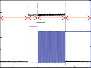
NATURE COMMUNICATIONS | DOI: 10.1038/s41467-017-00869-x                                                                                      ARTICLE

   Pulse parameters were carefully chosen to optimize bitrate and            efficiently save area of the circuits by 3D vertical stacking those
ensure the randomness of generated bits. We simulated three                  devices41.
possible cases during continuous pulse switching and identified                  We further characterize the operations of our diffusive mem-
two ways in which random number generation could fail: (i) no                ristor TRNG in response to two important challenges: tempera-
switching to the low resistive state during pulse, or (ii) insufficient       ture effects and long pulse cycling39. Our diffusive memristor
time to relax to the high resistive state during the inter-pulse             TRNG still functions satisfactorily and passes the NIST tests even
interval (Supplementary Fig. 9). Type (i) failure can be prevented           at 85 °C, as shown in the Supplementary Table 2. We collected
by choosing a sufficiently large pulse width and amplitude, such              11 M binary bits under 1 kHz pulses (voltage amplitude: 0.5 V
that the device will turn ON every cycle. Type (ii) failure can be           and pulse width: 300 µs). Unlike in operation at room tempera-
avoided by increasing the interval between pulses, so that the               ture, we can only collect the 3 lowest-order bits, which means the
device is always fully relaxed and nonzero delay time occurs                 bitrate decreases from 6 to 3 kb s−1. at 85 °C. However, this will
during every ON-switching cycle. This suggests that the pulse                not be a problem if we increase the clock frequency accordingly.
frequency and duration need be optimized to achieve the best                 Utilizing a clock signal of > 8 × 11.0592 = 88.4736 MHz, one will
performance of the diffusive memristor TRNG.                                 be able to keep the bitrate steady at 6 kb s−1. The required clock
   Randomness from volatile switching with a high ON/OFF ratio               frequency is dependent on the spread of delay time, and so the
is easier to exploit than small noises or current fluctuations. As a          decreased bitrate could be a result of the decreased s.d. of delay
result, simpler circuits are required. Our diffusive memristor               time at high temperatures. Possible degradation due to long pulse
TRNG can be built into memory subsystems, reducing chip area                 cycling is the other concern for memristive switching based
and increasing security. As revealed by simulations, the stochas-            TRNG39. We collected 54 M binary bits from a single diffusive
ticity is derived from the process of ionic motion, which suggests           memristor before the device failed and got stuck at ON state (each
that our diffusive memristor TRNG (like all other memristive-                cycle produced 6 random bits with endurance of ~ 107 cycles).
switching-based TRNG) could be more resistant to harsh envir-                Supplementary Table 3 shows that the total 54 M random bits
onments than other electron-based TRNGs36. Moreover, varying                 successfully passed all 15 NIST tests. In addition, we run the tests
temperature, when TRNG is operating, affects the distribution by             with the first 2 M bits from the initial cycles and the last 2 M bits
shifting its maximum towards lower time delays (see experiments              from the same device after ~ 9 × 10⁶ continuous cycles (Supple-
and simulations, Supplementary Fig. 6). However, the high fre-               mentary Table 4). Both of them passed all 15 tests, which strongly
quency clock used to generate random numbers makes sure the                  suggests that the randomness in memristors is still sufficient to
randomness is not affected.                                                  generate high quality random bits even after long cycling using
   Current bit generation rate from our diffusive memristor                  our method and again highlights the feasibility and novelty
TRNG is 6 kb s−1, which is sufficient for many encryption                     compared with previous attempts to build memristive switching
applications such as internet secure session link (SSL) keys, car            based TRNG29–31, 33, 39.
keys, and identification cards9, 29. To further increase the bit rate            In conclusion, we proposed and experimentally demonstrated
for other applications, a counter with more bits can be used in the          a novel diffusive memristor true random number generator
circuit. Supplementary Fig. 10 shows the comparison between                  (diffusive memristor TRNG) utilizing the stochastic delay time as
frequency counts of 8-bit block values if the 8-lower-order bits             the source of randomness. Our diffusive memristor TRNG has a
each cycle are collected and those of 6-bit block values from only           simple structure, and shows evident advantages in circuit com-
6-lowest-order bits. Clearly, frequency counts of 6-bit block                plexity, scalability, and power consumption. Binary bit sequences
values are uniform but those for the 8-bit block values are not,             generated by our diffusive memristor TRNG passed all the 15
which is because those two higher-order bits (7th and 8th) do not            NIST Special Publication 800-22 randomness tests without any
flip frequently enough under the current clock signal. The 8th                post-processing, a first for hardware utilizing memristive
lowest bit flips 4 times slower than the 6th lowest bit. To make              switching. Efficient approaches to further improve the bit
sure the two higher order bits also can flip more, we need                    generation rate are discussed. Finally, the physical nature of
to increase the clock frequency by a factor of about four                    stochastic delay time during ON-switching in these devices
(11.0592 × 4 = 44.2368 MHz) for an 8-bit counter. In general,                was explained by nanoparticle dynamics simulation and
a higher frequency clock signal is needed so that higher order bits          simple analytical estimates and attributed to the ionic/atomic
can also flip frequently to guarantee the generation of high quality          motion process, indicating our diffusive memristor TRNG
random bit streams. This comes at the cost of increased power                could be immune to harsh environments in contrast to
consumption. Alternatively, our diffusive memristor TRNG can                 other electron-based TRNGs. This is the first time that the true
be combined with a linear-feedback shift register (LFSR) for                 randomness of switching variability in memristors has been
higher bit rates with little increase in power consumption. We               confirmed with a standard test suite, which paves the way for the
performed simulation with MATLAB and demonstrated the                        adoption of memristors for more security applications for the era
bitrate can be readily increased by 50 times (to 300 kb s−1) with            of the IoT.
this method (Supplementary Note 4, Supplementary Fig. 11 and
Supplementary Table 1). With further optimization, such as using             Methods
a LFSR with more bits, the bitrate can potentially reach over                Device fabrication. We used Si wafers that have 100 nm thermally grown SiO2 on
100 MHz as previously reported29. In addition to circuit solu-               top as the substrates. For the 5 × 5 µm2 micro-devices, the bottom electrodes were
tions, device engineering that leads to a higher switching speed of          patterned by ultraviolet photolithography. After that, a 1.5 nm thick Ti adhesion
                                                                             layer and a 15 nm thick Pt bottom electrode were deposited sequentially in an
the diffusive memristors will also improve the bitrate without               electron beam evaporator, followed by a lift-off process in acetone. A 10 nm Ag:
changing the TRNG circuit. Possible solutions include changing               SiO2 blanket layer was prepared by radio-frequency (RF) co-sputtering from SiO2
the switching matrix35, 40 or using other memristive devices. For            and Ag targets (power for SiO2: 270 W and Ag: 12 W). Top electrodes were defined
instance, NbO2 could be a good candidate for the TRNG because                by a second photolithography step and a 15 s O2 descum, metallization of 5 nm Ag
                                                                             using RF sputtering (100 W) and 20 nm Pt/30 nm Au deposition using electron
of its sub-nanosecond switching speed, albeit with relatively high           beam evaporator and liftoff. The extra Ag layer was used as Ag ions reservoir while
operation current ( ~ 300 µA) and voltage ( ~ 1.5 V) even with               the Au layer was to improve the contact between pads and probe tips.
small device size20. Finally, parallel operation of several diffusive
memristors could also lead to increased bitrates by simulta-                 Electrical characterization. The DC electrical characterizations were carried out
neously generating multiple random sequences. One can                        using a Keysight B1500 semiconductor parameter analyzer in a voltage-sweep

NATURE COMMUNICATIONS | 8: 882    | DOI: 10.1038/s41467-017-00869-x | www.nature.com/naturecommunications                                                     7
ARTICLE NATURE COMMUNICATIONS | DOI: 10.1038/s41467-017-00869-x
mode. Voltage pulses were generated through a Keysight 33220A function/arbi- locations. A simple consideration of a circuit consisting of the memristor resistance
trary waveform generator while the output waveforms were monitored by a Key- connected in parallel to the memristor capacitance result in the equation for
sight MSO-X 3104 T mixed signal oscilloscope. During all the electrical voltage drop V(t) across the memristor:
measurements, the bottom electrodes were connected to a resistance to ground
dV Rex
while the top electrodes were biased. τ0 ¼ Vex ðt Þ 1 þ V ð6Þ
dt RðxÞ
Physical characterization. The XPS depth profile was acquired in a Physical where “RC” time τ0 = CMRex with the resistance Rex of external wires connected in
Electronics Instruments (PHI) quantum 2000. sequence with the memristor (for simulations we used κτ0 = 16 and RRmin
ex
¼ 0:5), and
Vex describes the applied voltage pulses.
NIST Randomness tests. A microcontroller (IAP15F2K61S2) was introduced to
collect a large number of bits from our diffusive memristor TRNG. To generate Data availability. The data that support the findings of this study are available
those sequences, input pulses (0.5 V, pulse width: 300 µs) at a frequency of 1 kHz from the corresponding author upon request.
were continuously sent to the diffusive memristor and a series resistor. We used the
microcontroller’s built-in 16-bit counter (11.0592 MHz) as the clock signal and
collected the 6 lower-order bits (6 kb s−1). NIST Statistical Test Suite (Special Received: 6 February 2017 Accepted: 1 August 2017
Publication 800-22) was downloaded from the NIST websites and then run in
virtual Linux system machine using the GNU Compiler Collection compiler. The
test suite contains 15 randomness tests and each test targets a specific aspect of
randomness. Each test returned two statistics, P-value (except non-overlapping-
template and random excursions variant) and pass rate. The bits are considered to
References
1. Weber, R. H. & Weber, R. Internet of Things, Vol. 12. (Springer, 2010).
be random if and only if the P-value ≥ 0.0001 and the pass rate exceeds the
2. Evans, D. The internet of things: how the next evolution of the internet is
minimum pass rate for each test.
changing everything. Cisco 1–11 (2011).
3. Van der Leest, V., Maes, R., Schrigen, G. J. & Tuyls, P. Hardware intrinsic
Diffusive memristor dynamical simulations. To simulate resistive switching in security to protect value in the mobile market. ISSE 2014 Securing Electronic
the diffusive memristor, we generalize the model used in ref. 34 where electric, heat Business Processes (Springer Vieweg, Wiesbaden, 2014).
and Ag-nanoparticle degrees of freedom were considered. In contrast to ref. 34 we 4. Bucci, M., Germani, L., Luzzi, R., Trifiletti, A. & Varanonuovo, M. A high-speed
have also taken into account the memristor self-capacitance, which is critically oscillator-based truly random number source for cryptographic applications on
important to describe the delay time distributions. The diffusion of Ag- a smart card IC. IEEE Trans. Computers 52, 403–409 (2003).
nanoparticles is described by the Langevin equations: 5. Petrie, C. S. & Connelly, J. A. A noise-based IC random number generator for
dxi ∂U ðxi Þ V ðt Þ pffiffiffiffiffiffiffiffiffiffiffiffiffi applications in cryptography. IEEE Trans. Circuits and Systems I 47, 615–621
η ¼ þα þ 2ηkB T ζ ð4Þ (2002).
dt ∂xi L
6. Tokunaga, C., Blaauw, D. & Mudge, T. True random number generator with a
where xi describes the location of the ith Ag-nanoparticle, t is time, and η is the metastability-based quality control. Proc. ISSCC 44, 404–405 (2007).
viscosity of Ag-nanoparticles. The potential profile U(xi), where Ag nanoparticles 7. Brederlow, R., Prakash, R., Paulus, C. & Thewes, R. A low-power true random
diffuse, is formed due to interfacial interactions (see Discussion in Supplementary number generator using random telegraph noise of single-oxde-traps. IEEE
Note 1 and Supplementary Fig. 12) attracting small particles to the Ag-electrode International Solid-State Circuits Conference Digest of Technical Papers (ISSCC),
and to the large cluster located near the electrode as well as large number of small 1666–1675 (San Francisco, CA, USA, 2006).
minima due to pinning of Ag-nanoparticles to the device inhomogeneities and 8. Yasuda, S. et al. Physical random number generator based on MOS structure
SiO2 matrix structure as well as repulsion from Pt-electrode. The particular shape after soft breakdown. IEEE J. Solid State Circ. 39, 1375–1377 (2004).
of potential (the potential profile used in simulations is shown in Fig. 4f) does not 9. Liu, N., Pinckney, N., Hansen, S., Sylvester, D. & Blaauw, D. 2011 Symposium
significantly affect the result. The only important property of the potential is the on VLSI Circuits 216–217 (Honolulu, HI, USA, 2011).
large minima associated with interfacial energy comparing with both temperature 10. Yang, K. et al. A 23Mb/s 23pJ/b fully synthesized true-random-number
and depths of multiwell pinning potentials; the repulsive potential barrier of the Pt- generator in 28 nm and 65 nm CMOS. IEEE International Solid-State Circuits
electrode should be strong enough to ensure relaxation to high resistive state on a Conference Digest of Technical Papers (ISSCC) 280–281 (San Francisco, CA,
reasonable time scale when no voltage is applied. The second term in the right- USA, 2014).
hand-side of eq. (4) is related to the electric bias/tilt of the potential in the electric 11. Fujita, S. et al. Si nanodevices for random number generating circuits for
field VLðt Þ if Ag-nanoparticles accumulate effective charge α (the strength of this cryptographic security. IEEE International Solid-State Circuits Conference
electric force tilt of the potential used in simulation is given in Supplementary Digest of Technical Papers (ISSCC) 294–295 (San Francisco, CA, USA, 2004).
Fig. 8a (inset)). The last term in Eq. (4) represents the unbiased δ-correlated white 12. Srinivasan, S. et al. 2.4GHz 7mW all-digital PVT-variation tolerant true
noise ζ: hζ ðt Þi ¼ 0; hζ ð0Þζ ðt Þi ¼ δðt Þ. The noise intensity is controlled by the random number generator in 45nm CMOS. Symposium on VLSI Circuits
temperature T (see Fig. 4f to estimate kBT0 with the Boltzmann constant kB and the 203–204 (Honolulu, HI, USA, 2010).
background temperature T0 with respect to the potential used in the simulations). 13. Fukushima, A. et al. Spin dice: a scalable truly random number generator based
In particular, the noise is responsible for overcoming the interfacial barrier which is on spintronics. Appl. Phys. Express 7, 083001 (2014).
suppressed by the electric force (in the simulations the electric field decreases the 14. Chua, L. O. Memristor-the missing circuit element. IEEE Transac. Circ. Theory
interfacial potential well by a factor of 1.6 at Vth); this results in switching the 18, 507–519 (1971).
system to its low resistance state when a voltage pulse is applied. In addition, the 15. Strukov, D. B., Snider, G. S., Stewart, D. R. & Williams, R. S. The missing
noise generates the diffusion of Ag-nanoparticles towards the Ag-electrode when memristor found. Nature 453, 80–83 (2008).
voltage is off resulting in the thermal relaxation of the memristors. 16. Yang, J. J., Strukov, D. B. & Stewart, D. R. Memristive devices for computing.
The heat dynamics in the memristor are described by Newton’s cooling law: Nat. Nanotechnol. 8, 13–24 (2013).
dT 17. Chang, T., Yang, Y. & Lu, W. Build neuromorphic circuits with memristive
¼ C1
T Q κ ðT T0 Þ
ð5Þ devices. IEEE Circ. Syst. Magazine 13, 56–73 (2013).
dt
18. Pi, S., Ghadiri-Sadrabadi, M., Bardin, J. C. & Xia, Q. Nanoscale memristive
where CT is the memristor heat capacitance, Q ¼ V ðt Þ2 =Rðx1 ; x2 ; ::; xN Þ is radiofrequency switches. Nat. Commun. 6, 7519 (2015).
Joule heat power with memristor resistance Rðx1 ; x2 ; ::; xN Þ, which depends on Ag- 19. Valov, I., Waser, R., Jameson, J. R. & Kozicki, M. N. Electrochemical
nanoparticle locations, κ is the heat transfer coefficient describing heat flux from metallization memories-fundamentas, applications, prospects. Nanotechnology.
the device. Note that the actual system temperature and the macroscopic-cluster 22, 254003 (2011).
temperature can be significantly different. We assume the resistance has a 20. Pickett, M. D. & Williams, R. S. Sub-100 fJ and sub-nanosecond thermally
tunneling nature and is described by the equation RðxÞ ¼ Rðx1 ; x2 ; ::; xN Þ ¼ driven threshold switching in niobium oxide crosspoint nanodevices.
P
N Nanotechnology. 23, 215202 (2012).
Rt eðxiþ1 xi Þ=λ where x0 and xN+1 are positions of the device terminals, Rt 21. Torrezan, A. C., Strachan, J. P., Medeiros-Ribeiro, G. & Williams, R. S. Sub-
0
resistance amplitude and λ is the tunneling length. The minimum possible nanosecond switching of a tantalum oxide memristor. Nanotechnology. 22,
resistance occurs when all Ag-nanoparticles are equally separated and has the value 485203 (2011).
Rmin ¼ ðN þ 1ÞRt eðxNþ1 x0 Þ=ððNþ1ÞλÞ (we used λ/L = 0.12 for 1D and 0.2 for 3D 22. Lee, M. J. et al. A fast, high-endurance and scalable non-volatile memory device
simulations). made from asymmetric Ta2O(5-x)/TaO(2-x) bilayer structures. Nat. Mater. 10,
As a distributed system with high resistance the memristor can have a 625–630 (2011).
capacitance (CM) which was not considered in previous models34, 35. In general, 23. Pi, S., Lin, P. & Xia, Q. Cross point arrays of 8 nm×8 nm memristive devices
this capacitance could be different in the two memristor states37, 38, but we, for fabricated with nanoimprint lithography. J. Vacuum Sci. Technol. B
simplicity, assume that CM is a constant and is not a function Ag nano-particle Microelectron. Nanometer Struct. 31, 06FA02 (2013).
8 NATURE COMMUNICATIONS | 8: 882 | DOI: 10.1038/s41467-017-00869-x | www.nature.com/naturecommunicationsNATURE COMMUNICATIONS | DOI: 10.1038/s41467-017-00869-x ARTICLE
24. Xia, Q. et al. Memristor−CMOS hybrid integrated circuits for reconfigurable Acknowledgements
logic. Nano. Lett. 9, 3640–3645 (2009). This work was supported in part by the U.S. Air Force Office for Scientific Research
25. Guan, X., Yu, S. & Wong, H. S. P. On the switching parameter variation of (AFOSR) (Grant No. FA9550-12-1-0038), the U.S. Air Force Research Laboratory
metal-oxide RRAM—part I: physical modeling and simulation methodology. (AFRL) (Grant No. FA8750-15-2-0044), and the National Science Foundation (NSF;
IEEE Transac. Electron Devices 59, 1172–1182 (2012). ECCS-1253073). D.B. is supported by a Research Experience for Undergraduates (REU)
26. Gaba, S., Sheridan, P., Zhou, J., Choi, S. & Lu, W. Stochastic memristive deviecs supplement grant from NSF. Any opinions, findings and conclusions or recommenda-
for computing and neuromorphic applications. Nanoscale 5, 5872–5878 (2013). tions expressed in this material are those of the authors and do not necessarily reflect the
27. Chen, A. Utilizing the variability of resistive random access memory to views of AFRL. We thank C. Yu and Dr. Xiaolin Xu for helpful discussions.
implement reconfigurable physical unclonable functions. IEEE Electron Devices
Lett. 59, 1172–1182 (2012).
28. Liu, R., Wu, H., Pang, Y., Qian, H. & Yu, S. Experimental characterization of
physical unclonable function based on 1kb resistive random access memory
Author contributions
Q.X. and H.J. conceived the idea, Q.X., J.J.Y. and H.J. designed the experiments. H.J.
arrays. IEEE Electron Devices Lett. 36, 1380–1383 (2015).
performed device fabrication and engineering. D.B. and S.L. built the circuit. H.J., D.B.
29. Huang, C. Y., Shen, W. C., Tseng, Y. H., King, Y. C. & Lin, C. J. A contact-
and S.L. performed electrical measurements. S.E.S. performed the simulation and
resistive random-access-memory-based true random number generator. IEEE
modeling. Z.W., Y.L., S.J., R.M. and C.L. helped with experiments and data analysis.
Electron Devices Lett. 33, 1108–1110 (2012).
Q.X., H.J., S.E.S. and J.J.Y. wrote the manuscript. All authors discussed the results,
30. Balatti, S., Ambrogio, S., Wang, Z. & Ielmini, D. True random number
commented on and gave approval to the final version of the manuscript.
generation by variability of resistive switching in oxide-based devices. IEEE J.
Emerg. Select. Top. Circuits Syst. 5, 214–221 (2015).
31. Balatti, S. et al. Physical unbiased generation of random numbers with coupled
resistive switching devices. IEEE Transac. Electron Devices 63, 2029–2035 (2016). Additional information
32. Rukhin A. et al. A statistical test suite for random and pseudorandom number Supplementary Information accompanies this paper at doi:10.1038/s41467-017-00869-x.
generators for cryptographic applications. NIST, Special Publication 800–822, (2010).
33. Wei, Z. et al. True random number generator using current difference based on Competing interests: The authors declare no competing financial interests.
a fractional stochastic model in 40-nm embedded ReRAM. IEEE Electron. Dev.
Meet. 4.8.1–4.8.4 (San Franciso, CA, USA, 2016). Reprints and permission information is available online at http://npg.nature.com/
34. Wang, Z. et al. Memristors with diffusive dynamics as synaptic emulators for reprintsandpermissions/
neuromorphic computing. Nat. Mater. 16, 101–108 (2017).
35. Midya, R. et al. Anatomy of Ag/Hafnia-based selectors with 1010 nonlinearity. Publisher's note: Springer Nature remains neutral with regard to jurisdictional claims in
Adv. Mater. 29, 1604457 (2016). published maps and institutional affiliations.
36. Fang, R. et al. Total ionizing dose effect of γ-ray radiation on the switching
characteristics and filament stability of HfOx resistive random access memory.
Appl. Phys. Lett. 104, 183507 (2014).
37. Salaoru, I., Li, Q., Khiat, A. & Prodromakis, T. Coexistence of memory Open Access This article is licensed under a Creative Commons
resistance and memory capacitance in TiO2 solid-state devices. Nanoscale Res. Attribution 4.0 International License, which permits use, sharing,
Lett. 9, 552–558 (2014). adaptation, distribution and reproduction in any medium or format, as long as you give
38. Bessonov, A. A. et al. Layered memristive and memcapacitive switches for appropriate credit to the original author(s) and the source, provide a link to the Creative
printable electronics. Nat. Mater. 14, 199–204 (2015). Commons license, and indicate if changes were made. The images or other third party
39. Gallo, M. L., Tuma, T., Zipoli, F., Sebastian, A., Eleftheriou, E. Inherent material in this article are included in the article’s Creative Commons license, unless
stochasticity in phase-change memory devices. in 46th European Solid State indicated otherwise in a credit line to the material. If material is not included in the
Device Research Conference (ESSDERC), 373–376 (Lausanne, Switzerland, 2016). article’s Creative Commons license and your intended use is not permitted by statutory
40. Song, J. et al. Monolithic integration of AgTe/TiO2 based threshold switching regulation or exceeds the permitted use, you will need to obtain permission directly from
device with TiN liner for steep slope field-effect transistors. IEEE International the copyright holder. To view a copy of this license, visit http://creativecommons.org/
Electron Devices Meeting (IEDM) 25.3.1–25.3.4 (San Francisco, CA, USA, 2016). licenses/by/4.0/.
41. Baek, I. G. et al. Realization of vertical resistive memory (VRRAM) using cost
effective 3D process. IEEE International Electronic Devices Meeting (IEDM).
31.8.1–31.8.4 (Washington, DC, USA, 2011). © The Author(s) 2017
NATURE COMMUNICATIONS | 8: 882 | DOI: 10.1038/s41467-017-00869-x | www.nature.com/naturecommunications 9You can also read