Analysis and Characterization of Normally-Off Gallium Nitride High Electron Mobility Transistors
←
→
Page content transcription
If your browser does not render page correctly, please read the page content below
Computers, Materials & Continua                                                             Tech Science Press
DOI:10.32604/cmc.2021.018248
Article

  Analysis and Characterization of Normally-Off Gallium Nitride High Electron
                              Mobility Transistors
        Shahzaib Anwar1 , Sardar Muhammad Gulfam1, * , Bilal Muhammad2 , Syed Junaid Nawaz1
                            Khursheed Aurangzeb3 and Mohammad Kaleem1

        1
         Department of Electrical and Computer Engineering, COMSATS University Islamabad (CUI), Islamabad,
                                                    45550, Pakistan
2
  CTIF Global Capsule, Department of Business Development and Technology, Aarhus University, 7400, Herning, Denmark
    3
      Computer Engineering Department, College of Computer and Information Sciences, King Saud University, Riyadh,
                                                  11543, Saudi Arabia
             *
               Corresponding Author: Sardar Muhammad Gulfam. Email: sardar_muhammad@comsats.edu.pk
                                    Received: 02 March 2021; Accepted: 08 April 2021

                  Abstract: High electron mobility transistor (HEMT) based on gallium nitride
                  (GaN) is one of the most promising candidates for the future generation of
                  high frequencies and high-power electronic applications. This research work
                  aims at designing and characterization of enhancement-mode or normally-off
                  GaN HEMT. The impact of variations in gate length, mole concentration,
                  barrier variations and other important design parameters on the performance
                  of normally-off GaN HEMT is thoroughly investigated. An increase in the
                  gate length causes a decrease in the drain current and transconductance,
                  while an increase in drain current and transconductance can be achieved by
                  increasing the concentration of aluminium (Al). For Al mole fractions of 23%,
                  25%, and 27%, within Al gallium nitride (AlGaN) barrier, the GaN HEMT
                  devices provide a maximum drain current of 347, 408 and 474 mA/μm and a
                  transconductance of 19, 20.2, 21.5 mS/μm, respectively. Whereas, for Al mole
                  fraction of 10% and 15%, within AlGaN buffer, these devices are observed
                  to provide a drain current of 329 and 283 mA/μm, respectively. Furthermore,
                  for a gate length of 2.4, 3.4, and 4.4 μm, the device is observed to exhibit
                  a maximum drain current of 272, 235, and 221 mA/μm and the transcon-
                  ductance of 16.2, 14, and 12.3 mS/μm, respectively. It is established that a
                  maximum drain current of 997 mA/μm can be achieved with an Al concen-
                  tration of 23%, and the device exhibits a steady drain current with enhanced
                  transconductance. These observations demonstrate tremendous potential for
                  two-dimensional electron gas (2DEG) for securing of the normally-off mode
                  operation. A suitable setting of gate length and other design parameters is
                  critical in preserving the normally-off mode operation while also enhancing
                  the critical performance parameters at the same time. Due to the normally-
                  on depletion-mode nature of GaN HEMT, it is usually not considered as
                  suitable for high power levels, frequencies, and temperature. In such settings,
                  a negative bias is required to enter the blocking condition; however, in the

                      This work is licensed under a Creative Commons Attribution 4.0 International License,
                      which permits unrestricted use, distribution, and reproduction in any medium, provided
                      the original work is properly cited.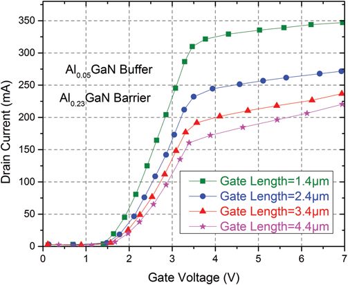
1022                                                                               CMC, 2021, vol.69, no.1

                 before-mentioned normally-off devices, the negative bias can be avoided and
                 the channel can be depleted without applying a negative bias.

                 Keywords: High electron mobility; GaN; HEMT; bipolar transistors
                 gallium nitride; heterojunctions; MOS devices

1 Introduction
     Today 40% of the energy consumed in the world is shared by electric energy. This share is
anticipated to increase further about by 60% in 2040 [1]. Modern societies will strongly depend
upon the production and management of electric energy. The electricity not only will have to be
produced with environmentally friendly approaches (e.g., favouring the renewable energies) but also
will have to be distributed and used more efficiently. Power Electronics is a key technology between
energy generation and end-user. Power electronic devices do energy conversion from direct current
(DC) to alternating current (AC), AC to DC and DC to AC according to requirements [2]. A large
portion (up to 54%) of the energy is dissipated in Silicon (Si) devices during electricity conversion
processes [3]. Swapping Silicon with wide bandgap semiconductors such as silicon carbide (SiC)
and gallium nitride (GaN) in power electronics can minimize 20%–25% of the overall electricity
consumption worldwide (with a potential saving of more than $30 billion/year) [4]. We can save
energy with power electronic devices by reducing the power loss and retaining the higher con-
version efficiency. The demand for highly efficient power electronic application goes on increasing
in consumer electronics with an increase in power consumption. The silicon-based devices can’t
be able to meet all requirements of higher voltage, higher current, large switching frequency and
higher efficiency.
    As compared to silicon, the energy bandgap of GaN is 3.4 eV which lies in wide bandgap
semiconductors and due to this reason gallium nitride high electron mobility transistor (GaN
HEMT) can be operated at high temperature, higher breakdown field, low on-resistance and high
Baliga figure of merit (BFOM) [5]. Material characteristics have a very significant influence on
the fundamental features of the device. Fig. 1 represents the comparison of four materials Si,
SiC, GaN and gallium arsenide (GaAs) in terms of the electric field, saturation velocity, melting
point and thermal conductivity. GaN has higher electric field and electron peak velocity which
results in higher electron mobility and low leakage current [6]. Moreover, GaN functions at high
voltages with low leakage current due to its higher breakdown electric field and it also operates
in higher frequencies because of its high electron mobility [7]. GaN represents excellent electrical
and physical characteristics than silicon. GaN is an exceptional material for large power and
high-frequency devices [8].
    GaN HEMTs are very similar to traditional field-effect transistors (FET). Like FET it has
also three terminals drain, source and gate which represent the subcategory of voltage-controlled
Power switches. The difference is, in HEMT we are using the heterojunction in between GaN and
aluminium gallium nitride (AlGaN) instead of a doped region in FET. Because of two operating
modes of GaN HEMTs, these are divided into two types of categories such as depletion-mode
or normally-on and enhancement-mode or normally-off. In the case of depletion-mode of GaN
HEMTs, the source and drain electrodes are placed in the barrier layer of AlGaN which is on the
uppermost side of GaN transistor to build the ohmic contact with two-dimensional electron gas
(2DEG) which is below the AlGaN layer [9]. In radio frequency (RF) applications, the depletion-
mode of GaN HEMTs is frequently used as power amplifies but has restricted applications in
power converters or power electronics [10].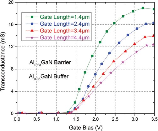
CMC, 2021, vol.69, no.1                                                                         1023

                          Figure 1: Material characteristics of GaN and Si [7]

    In the field of power electronics, during start-up of power converters, a negative bias should
be induced in gate otherwise a short circuit will happen. But enhancement-mode can be used
in power electronics application or power converters because this normally-off device would not
experience this constraint. Enhancement-mode of GaN HEMTs performs in an analogous way
to metal-oxide field-effect transistors (MOSFET) in which channel is not built-in like normally-
on GaN transistors, therefore, the positive voltage is applied at the gate terminal connecting the
source. This positive voltage attracts the electrons to form a bidirectional channel between the
source and drain. The entire resistance of the conducting channel becomes minimum because
of these electrons which are pooled in the 2DEG [11]. The device remains on till the positive
voltage connected to the gate terminal. Whenever voltage is detached from the gate, the device
turns into off condition because electrons beneath it disperse, removing the conductive channel.
In other words, if the gate bias entails the negative voltage, then the design is described as a
Depletion-mode design of HEMT. The electron carrier’s density inside the channel relies on the
voltage which has employed at the gate terminal [12]. The recent developed GaN HEMTs models
cannot work as a comprehensive design for GaN RF devices and GaN power devices due to
the complexity in the design construction. Various ML algorithms predict the output of a GaN
HEMT device by mapping the data into decision models [13].
     This paper is focused on designing and analysing the appropriate model of normally-off GaN
HEMTs with considering the suitable structural parameters such as gate length, aluminium mole
concentrations, buffer and barrier variations. The impact of these variations will be inspected
on electrical parameters such as drain current, transconductance and gate voltages. This paper
is arranged as follows. Section 2 reviews the detailed study of the evaluation of GaN HEMT
technology and a brief history of how normally-off structures were implemented with different
techniques. Section 3 introduces the device simulation mechanisms and deals with the implemen-
tation of a GaN HEMT structure using p-GaN gate technique to make device normally-off. Two
normally-off structures are studied and discussed in this section and their characteristics curves
are also analyzed. In Section 4, structural parameters are varied to analyse the impact on electrical
parameters. The effects of drain current on variations of aluminium concentrations in buffer
and barrier are investigated. Section 5 represents the effects of gate length on the drain current.
Section 6 discusses the effect of gate length and aluminium concentrations on transconductance.
Section 7 concludes the overall contribution of the paper.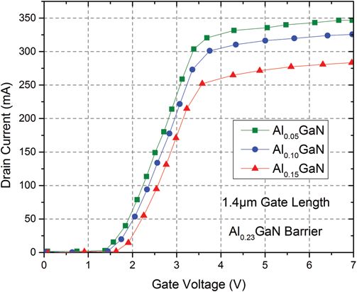
1024                                                                         CMC, 2021, vol.69, no.1

2 Background, State-of-the-Art and Future Outlook
     In the power electronics industry, silicon power devices have dominated the 20th century. In
the 1950s, bipolar power transistors (BJT) and Silicon controlled rectifier (SCR) were introduced.
Power electronics industry migrates to metal oxide silicon transistor (MOS) gated devices in the
1980s. Those applications which operate at a power supply voltage below 220 V, silicon power
MOSFET turn into a well-known device of choice. To remove most of the defects in silicon power
devices such as high on-state resistance insulated gate bipolar transistor (IGBT) was introduced in
the 1980s [14]. IGBTs minimizes the cost and reduces the extent of power electronic circuitry by
developing it more efficient technology for consumer and industrial users along with minimum on-
state voltage drop and excellent performance. To displace the broadly acknowledged technology,
new technology must propose significant perfections to the reduction in the on-state voltage and
switching losses, while preserving all the additional features [15]. Countless innovative concepts
were anticipated and established for silicon power devices that were accessible as products in the
1990s. For any novel anticipated expertise, it is necessary to exceed the fulfilment of not only
the old silicon power devices but be capable to contend with these more eminent productions of
silicon devices as well [14]. Based on elementary material properties of semiconductors, the first
examination related to the performance of power devices was established in 1980 and published
in 1982. To estimate the possible developments in the on-state resistance of FET based power
devices by adding silicon with different semiconductor substances formed a simple equation, now
usually referred to as BFOM. By swapping silicon with GaAs, this examination showed 13.7-times
improvement. GaAs based power devices beginning to emerge as a direct result of estimation in
the 1980s [16].
     Afterwards, GaAs power rectifiers having a breakdown voltage of 200 V have been developed
and accessible from numerous companies. Swapping silicon with extensive bandgap semiconductor
corporeality, these strategies represent the first-power semiconductor products [17]. In the 1990s,
improvement of unipolar devices of the existing hexagonal silicon carbide (6H-SiC) polytype
substance, BFOM for SiC provided the solid incentive for this cause. The initial device based on
SiC for operating in high-voltage up to 400 V as a Schottky rectifier of SiC along with minimum
on-state voltage drops up to 1 V is demonstrated by north Carolina state university (NCSU) in
1992 [18,19]. Attention in GaN raised in the 1990s because of its better capabilities for utilisation
in the illumination and cellular amplifier industries [20]. Marketable products created with this
substance have developed remarkable demands in these markets. Newly, important attention has
arisen in exploiting the new substance for constructing power devices that might potentially reach
the achievement of silicon-based power devices and be more extra cost effectual as compared
to silicon carbide power devices [17]. The GaN HEMT has been under examination because of
their outstanding performance in high power electronic devices. There is an essential need to
understand the operation of the device by designing a model which could be used to enhance
electrical features of GaN HEMT design for high power and high-frequency operation [21].
AlGaN/GaN heterostructures based HEMT have demonstrated greater performance than that of
Silicon counterparts at larger voltage, greater current and higher frequency and temperature [22].
This material has a stronger electric field with the advantage of the more mobility and electron
density of 2DEG developing at the AlGaN/GaN interface [23]. Normally-on mode AlGaN/GaN
HEMT is utilized for those applications which require minimum voltage and limited frequency
range. To use in power switching applications, enhancement-mode features are needed to assure
secure handling because of higher voltage [24].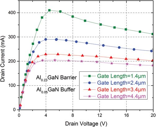
CMC, 2021, vol.69, no.1                                                                       1025

     Many techniques have been developed to obtain the normally-off GaN HEMT. By applying
the very small thin barrier layer of AlGaN with very depressed aluminium fractions, 2DEG
depletion can be achieved. The first genuine solution anticipated for enhancement-mode of GaN
HEMT was the depressed thin barrier layer below the critical thickness which is necessary for the
generation of such channel in the region under the gate terminal [25]. Normally-off behaviour of
GaN HEMTs can also be achieved by introducing the fluorine gas below the gate electrode [26,27].
Another approach of achieving the normally-off GaN HEMTs is to introduce the local surface
oxidation methods or interjecting the nitric oxide (NiOx) based interlayer under the gate to obtain
the positive Vth shift [28]. To overcome these various restrictions, the hybrid metal insulator
semiconductor high electron mobility transistor (MISHEMT) structures were developed [29]. The
AlGaN barrier layer is removed under the gate in this device establishing the channel employing
a metal-insulator semiconductor (MIS) system. Therefore, this method associates the benefits
of an enhancement-mode MIS channel having the least immunity of the 2DEG. Though, the
selection of the dielectric sheet is very crucial in GaN power designs and also necessary for MIS
HEMTs. It explicitly influences both the carrier movement and threshold voltage durability [30].
Possibly, the most capable technique is the usage of a p-GaN (or p-AlGaN) layer below the
gate contact region on the interface of AlGaN/GaN heterostructure. Without the presence of
an externally injected bias at gate terminal which means gate to the source, voltage is zero. The
channel becomes depleted of carriers at (VG = 0) due to the advancement of band diagram. As
a result, the exhaustion of the 2DEG channel occurs in this case. This method is getting a great
consideration within the scientific society because of this fact that barely “real” enhancement-
mode of GaN HEMT which is accessible to date on a commercial level is based on a p-GaN gate.
Although, enhancement-mode of HEMT technology with p-doped GaN is slightly complicated
and HEMT performance can be significantly affected by numerous design and processing circum-
stances. Many other significant safety features connected to the enhancement-mode of p-GaN gate
GaN HEMT technology with AlGaN buffer that includes threshold voltage and balance charge
trapping tools [31].
    The essential benefit of the GaN HEMT is that it has a considerably lesser figure of merit
(FOM) than that of silicon super-junction (SJ) and SiC-MOSFETs [23]. The switching FOM is
the multiplication of the gate charge and the resistance between the drain and source terminals
in the on-state [32]. 2DEG is produced by polarization effects of heterojunction within GaN
HEMT which shows the depletion-mode naturally normally-on behaviour of these devices that
exclude them from most power electronics applications [33]. For normally-off enhancement-mode
operation, the p-type layer of GaN or AlGaN is introduced under the gate metal in many reported
researches. GaN-based power semiconductors are largely adjacent structures [34]. GaN HEMT
models are usually analysed using Computer-aided design (CAD) based approaches.

3 Device, Design, Simulations and Characteristics
    In this section, we present the design analysis of enhancement-mode of GaN HEMT using
Technology computer-aided design (technology CAD or TCAD) which signifies a multipurpose
plus flexible program intended for two- and three-dimensional design modelling. The electric char-
acteristics of these enhancement-mode structures with different buffers, aluminium concentrations
and gate lengths are scrutinized with the help of ATLAS simulator which is more compact
and reliable. In this research, we consider the normally-off GaN HEMT model design in two-
dimensional matrix-mesh format [35]. Every mesh point denotes a physical location inside the
modelled design and program simulates transport characteristics through differential equations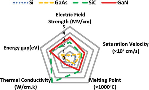
1026                                                                         CMC, 2021, vol.69, no.1

resulting from Maxwell’s equations at these mesh points [36]. Different numerical analyses are used
to solve for electrostatic potential and carrier densities within the design. Most commonly used
is the Newton Raphson method. Different parameters of normally-off GaN HEMT are studied
such as gate length, transconductance, drain current, gate voltage, aluminium mole fraction and
various other effects are also analysed while designing the enhancement-mode model.
    Two normally-off structures have been analysed due to normally-on behaviour of GaN
HEMT, using p-GAN gate where the gate is p-doped. One structure is designed using AlGAN
buffer with AlGAN barrier and GaN channel. The second GaN HEMT structure is based on
GaN buffer with AlGaN back barrier. The characteristic curves with AlGaN buffer are shown
in Fig. 3. The curves are plotted on different gate voltages. The drain current rises with growing
gate voltage at static drain voltage or fixed gate voltage with increasing drain voltage. With higher
gate voltages, more electrons are attracted into the bidirectional channel. This increased electron
density drives to accretion in drain current. The dimensions of the GaN HEMT device structure
With AlGaN Buffer are as follows [37]:

               Figure 2: The cross-sectional view of proposed GaN HEMT structure

    •   Source and drain lengths are 1 μm and widths are 110 nm.
    •   Gate length is 1.4 μm and Width is 100 nm.
    •   P-GaN layer length underneath the Gate is equal to gate length but width is 110 nm.
    •   The lengths of Al0.05GaN0.95 Buffer, GaN Channel, Al0.23GaN0.95 Barrier, and SiN
        Layer are 10.4 μm which is equal to device length.
    •   The width of Al0.05 GaN0.95 Buffer is 2 μm.
    •   The width of the GaN Channel is 35 nm.
    •   Width of Al0.23 GaN0.95 Barrier is 15 nm.
    •   The width of the SiN Layer is 35 nm.
    •   The total device width is 2.36 μm. Spacing between the source to the gate is 2 μm but the
        gate to drain is 5 μm.
    Another structure of enhancement-mode GaN HEMT transistor for power electronic applica-
tion with the modified GaN buffer and AlGaN back-barrier is manifested. It is also converted into
normally-off mode by introducing a p-GaN layer underneath the gate which depletes the channel
when the device is off [38]. By introducing the GaN buffer with AlGaN back-barrier, the device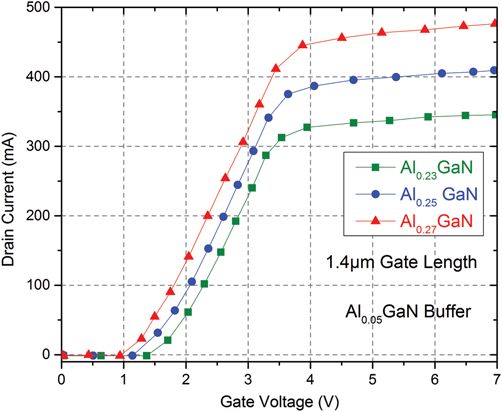
CMC, 2021, vol.69, no.1 1027
becomes more compatible with power electronic applications due to despicable on-state resistance,
the higher threshold voltage and securing the normally-off operation. The cross-sectional view of
the proposed structure is shown in Fig. 2 and its characteristic curves are shown in Fig. 3.
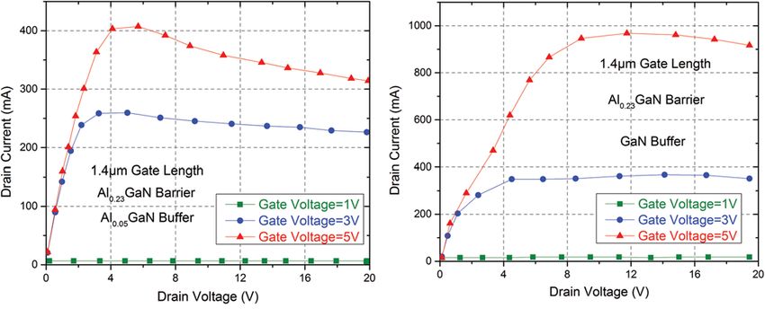
Figure 3: Simulation results for the impact of Drain Voltage and Gate Voltage on Drain Current
for the proposed GaN HEMT. (a) AlGaN buffer, (b) GaN buffer
Theses curves are also taken from three different gate voltages 1 v, 3 v and 5 v. In the
enhancement-mode structure, we have to apply the positive source to the gate voltage. The positive
voltage at the gate terminal produces the quantum well at the interface of AlGaN and GaN
structure. The electrons are attracted to that quantum well which leads to the formation of 2DEG.
Higher the positive voltage, higher will be the depth of quantum well and more will be the drain
current. This structure gives a higher drain current as compared to the previous model with the
same conditions. The high electron density is achieved in GaN HEMT because electrons flow
within the bidirectional channel separate from their donor atoms which minimize the collisions
and scattering of electrons [39]. As a result, the mobility of electrons has been increased. This
high mobility electrons start penetrating GaN buffer under the GaN channel and their mobility
is reduced inside the buffer. The concentration of electrons within the channel is also reduced.
Therefore, AlGaN back-barrier is introduced underneath the channel to concentrate the electrons
within the channel [40]. AlGaN back-barrier has higher energy level as compared to the channel
and electrons from the channel cannot jump to this barrier. The dimensions of the proposed
device structure for GaN HEMT With GaN Buffer are as follows:
• Source and drain lengths are 1 μm and widths are 110 nm.
• Gate length is 1.4 μm and Width is 100 nm
• P-GaN layer length underneath the Gate is equal to gate length but width is 110 nm.
• The lengths of Al0.05GaN0.95 Buffer, GaN Channel, Al0.23GaN0.95 Barrier, SiN Layer
are 10.4 μm which is equal to device length.
• The width of the GaN buffer is 2 μm.
• The width of the Al0.05GaN back-barrier is 35 nm.
• The width of the GaN Channel is 15 nm.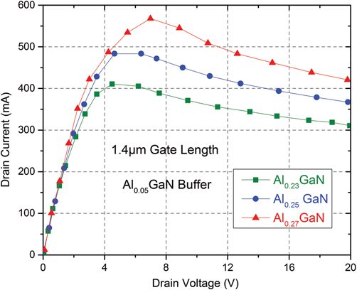
1028                                                                         CMC, 2021, vol.69, no.1

    • Width of Al0.23GaN0.95 Barrier is 15 nm.
    • The width of the SiN layer is 295 nm.
    • The total device width is 2.36 μm. Spacing between the source to the gate is 2 μm but the
      gate to drain is 5 μm.

4 Effects of Aluminium Mole Fractions
     The HEMT construction is based on phenomena of high electron mobility which described as
2DEG because of development of heterostructure in between the AlGaN and GaN [41]. 2DEG
flows in between this region of AlGaN and GaN. Due to placing the p-GaN under the gate, when
2DEG is unbiased, p-GaN layer accumulates the positive charge due to the impurity of a p-type
semiconductor, these positive charges deplete the electrons within the channel [42]. When two
different materials having large bandgap are combined while keeping equivalent crystal structure,
a heterostructure is formed and energy discontinuity is created in a band diagram. In conduction
band, the notch is produced and in the valence band, the valley is produced due to bandgap
discontinuity [31]. The difference of lattice constant determines the quality of junction produced
between such materials. Two materials having a larger difference between lattice constants, there
is a larger prospect of the interface defect [43]. The similarity in lattice constant is an essential
condition to develop suitable heterojunction and excellent heterostructure based design. If we
are combining the corporealities such as AlGaN and GaN, the only constraint which is to be
measured is the composition of aluminium since it expresses the bandgap energy and lattices
constant of AlGaN [44]. Variations of aluminium mole fraction exhibit different effects on AlGaN
barrier and buffer.

4.1 Barrier Effects
     Initially, we examine the effects of aluminium mole fraction (typically in the range from 15%–
20%) on AlGaN GaN-based GaN HEMT. In the heterojunction transistor, two materials with
different bandgaps, ensures that the work functions and electron affinities are combined. Electrons
are transferred from material to another. The material that donates electrons has to be a higher
bandgap and work function material as compared to that material which accepts the electrons.
The larger the bandgap difference between the materials, more electrons will be transferred to
the other material to balance the energy level and hence more will be the current. The bandgap
of AlGaN can vary from 3.4 eV to 6.2 eV depending upon the aluminium concentrations. The
resulting band structure of any heterojunction transistor estimates the electrical behaviour of any
device. The higher bandgap is produced with an increase in aluminium mole concentration in
AlGaN barrier layer which leads to more increase in conduction band discontinuity that appears
in greater confinement of carriers in the channel in between AlGaN and GaN, providing large
mobility to accompany with a high electron density [44].
    Effect of aluminium concentration in the barrier layer of GaN HEMT with (20% or higher)
was recorded in the last few years. It is necessary to examine systematically the dependency of
aluminium mole fraction in the barrier layer of GaN HEMT. The structure parameters such as
aluminium mole concentrations are to be varied to study the effects on electrical parameters such
as drain voltage and current as well as gate voltage and current. We can control the drain current
by varying the aluminium fractions. Drain voltage and drain current are directly proportional to
each other. If we kept the gate voltage constant, drain current tends to increase with an increase
in drain voltage. The gate voltage is also proportional to the drain current. If we increase the
gate voltage by keeping the drain voltage constant, drain current increases. Simulation results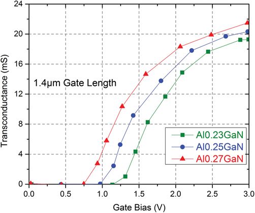
CMC, 2021, vol.69, no.1                                                                        1029

show the drain current also increases with an increase in aluminium concentration in the AlGaN
barrier [45].
     The maximum drain current is 347 mA with the aluminium mole fraction of 0.23. The drain
current increases up to 408 mA with the aluminium mole fraction of 0.25 which further increases
up to 474 mA with the aluminium mole fraction of 0.27 as shown in Figs. 4 and 5. Electron
density in the 2DEG of the transistor channel is reduced giving high threshold voltage due to
low aluminium concentrations in AlGAN barrier. The drain current goes on in-creasing with
increasing aluminium fraction in the barrier [46]. These results are taken by applying the three
different aluminium concentrations with fixed drain voltages. These show that, with an increase
in aluminium concentrations, more electrons accumulate in the bidirectional channel and drain
current increases with it. Hence, relatively high aluminium mole fraction is introduced within the
AlGaN barrier to achieve high electron density in 2DEG within GaN channel [42].

Figure 4: Effects of aluminium concentration in AlGaN barrier (drain voltage vs. drain current)

4.2 Buffer Effects
    The Effect of aluminium fractions in the buffer is quite different as compared to the barrier.
    The drain current decreases with more addition in aluminium mole fractions [47]. With an
increase in aluminium concentration in AlGaN buffer, the buffer energy level is enhanced due to
the increase in the bandgap. Since electrons tend to transfer from higher bandgap material to the
lower one.
    Therefore, now electrons are transferred from AlGaN buffer to the GaN Chanel in which
2DEG is already built-in due to electrons. The scattering of electrons has been increased due to
repulsions and collision effects. If the buffer layer energy level equals to channel, some electrons
enter into the buffer from the channel due to high mobility of 2DEG. Hence AlGaN buffer
must have the slighter higher energy level than the GaN channel to avoid these penetrations.
Back-barrier of higher bandgap with GaN buffer can also be used. Neither electrons from the
GaN channel nor GaN buffer can cross back-barrier. Mobility of electrons and drain current
are increased in these configurations. The maximum drain current is 342 mA with the aluminium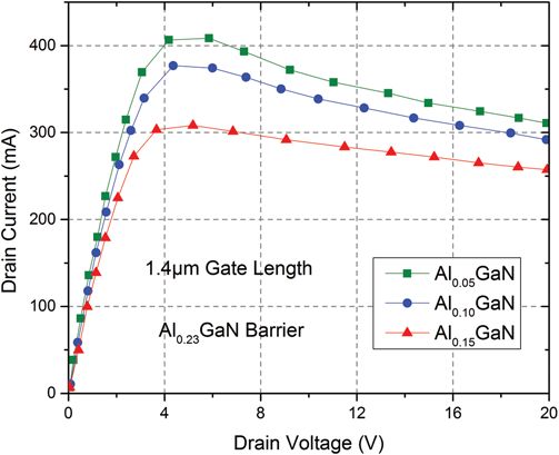
1030                                                                        CMC, 2021, vol.69, no.1

mole fraction of 0.07 and maximum drain current decreases to 329 mA with the aluminium
mole fraction of 0.10 which further decreases to 283 mA when aluminium mole fraction further
increases to 0.15 as shown in Figs. 6 and 7. Drain current reduces due to the reduction in electron
density within the channel between the AlGaN and GaN. The electron density within the channel
is slightly reduced due to the increase in aluminium concentration in the buffer of GaN HEMT.
Hence a minimum aluminium concentration in AlGaN buffer underneath the GaN channel is
subject to obtain the high electron density in 2DEG [48].

 Figure 5: Effects of aluminium concentration in AlGaN barrier (gate voltage vs. drain current)

Figure 6: Effects of aluminium concentration in AlGaN buffer (drain voltage vs. drain current)
CMC, 2021, vol.69, no.1                                                                         1031

 Figure 7: Effects of aluminium concentration in AlGaN buffer (gate voltage vs. drain current)

5 Effects of Gate Length on Drain Current
     Influence of variation in p-GaN gate dimension has studied to understand the reliability of
this device. By increasing the gate length, drain current decreases because of lowering the density
of 2DEG within the channel under the gate that diminishes the drain current. The reduced gate
length is larger acceptable for power electronic applications [49].
    The drain current (Id) is represented in the equations given below according to the article of
Charfeddine et al. [50].
     zuBe             vd
Id =        vg − vth −      vd                                                                  (1)
      Lg               2

     In above relations, Lg represents the gate length, Vg, Vth and Vd represent the gate voltage,
threshold voltage and drain voltage respectively. Z is channel width and μ is the mobility of
carriers.

                      2
Ids = BuF      vg − vth + F Lg − FLg
                            2  2                                                               (2)

     The maximum saturation drain current is represented in the above equation. Where F is the
critical electric field. According to previous analytical modelling of Charfeddine, drain current and
gate length are inversely proportional to each other. Drain current minimizes with increase in gate
length. Simulation results have shown in Fig. 8 which matches with this analytical modelling that
shows drain current reduces by increasing the gate dimensions. With the variation of 1 μm in gate
length, the drain current reduces from 347 mA/μm to 272 mA/μm due to decrease in the deepness
of quantum well. This is essentially due to the reduction of confinement of carriers because the
gate length of the p-GaN gate is increased. This phenomenon leads to a reduction in the intensity
of 2DEG within the GaN channel which indeed lessens the drain current inside the channel. From
the simulation results shown below, it can be concluded that whenever the gate length is expanded
to a certain limit, the chances of the controllability of the electric field has enhanced below the
1032 CMC, 2021, vol.69, no.1
channel generated by the gate contact. Therefore, Peak value of the electric field has reduced and
it leads to increase the regularity of the electric field beneath the gate contact. The passage of
electrons accompanying the 2DEG inside the channel becomes more complicated which leads to
a decline in maximum current density. After a certain point, also known as an optimum point,
there is less significant variation in the maximum current density when the gate length is increased
beyond the optimum point. Because after achieving the minimum possible gate length, the electric
field beneath the channel generated by gate contact takes no much variations.
Figure 8: Effect of gate lengths on drain current (drain voltage vs. drain current)
Figure 9: Effect of gate lengths on drain current (gate voltage vs. drain current)CMC, 2021, vol.69, no.1 1033
Further, the drain current becomes 235 mA/μm when gate length increases to 3.4 μm. This is
less decrease as compared to the previous one because more increase in gate length, the closer will
be the optimum point. The drain current reduces to 221 mA/μm when the gate length is further
extended to 4.4/μm as shown in Fig. 9.
6 Effects of Gate Length and Aluminium Concentration on Transconductance
Transconductance is the characteristic of several power electronic components. As Con-
ductance is complementary of resistance, therefore, transconductance is the proportion of the
variation in current at the output terminal to the variation in voltage at the input terminal. It is
formulated as gm. Transconductance is the function of the gate length.
I
gm = (3)
v
The transconductance modifications for varying gate lengths have conferred in Fig. 10. It has
been observed that by increasing the gate length from 1.4 μm to 3.4 μm, the transconductance
reduces due to decrease in the drain current with an increase in gate length. We can infer from
these simulations result that minimum gate expansion is more suitable and compatible for immense
power and switching applications.
Figure 10: Effect of gate lengths on transconductance
From simulation results shown in Fig. 7 and also from previous obtained results it can
be observed that after increasing the gate length with certain limit, the passage of electron in
2DEG is more complicated and due to this transconductance decreases similar to drain current.
Transconductance decreases up to the optimum point after which there is no much variation of
transconductance when the gate length is beyond the optimum point. At 1.4 μm gate length,
the value of transconductance is 19 ms/μm which decreases to 16 ms/μm when the gate length
is 2.4 μm but this decrease is much less as we further increase the gate length up to 4.4
μm. The transconductance modifications for varying aluminium concentrations in the AlGaN
barrier have presented in Fig. 11. Since the drain current increases with an increase in aluminium1034 CMC, 2021, vol.69, no.1
concentrations, therefore transconductance gradually tends to increase with an increase in drain
current.
Figure 11: Effect of aluminium concentrations on transconductance
The conducted study is of high significance in designing the appropriate model of GaN
HEMT for next-generation power electronics. This permits power electronic projects at higher
frequencies that enable a reduction in the size and cost of devices. The smaller size of devices
with high power rating revolutionizes the field of electronics. These devices can operate on high
switching speed and having low leakage current due to reduction in intrinsic carrier concentrations.
The conducted analysis can help in meeting the increasing stringent performance and design
requirements of electronic materials in terms of higher conversion efficiency with lower energy
loss, cost and size of power devices.
7 Conclusion
In this research work, the analysis of the proposed design of normally-off GaN HEMT has
been presented for power electronic applications. The electrical parameters such as drain current,
gate voltage and transconductance have been analysed by varying the structural parameters which
include gate length, aluminium mole concentration in buffer and barrier and by applying the
different types of buffers. With more addition of aluminium concentration in the buffer, the drain
current can be reduced due to the decrease in the electron density within the channel. The drain
current always tends to increase with an increase in aluminium mole concentrations within the
barrier. The variation of gate length has also impacted on the behaviour of drain current. Drain
current reduced with an expanding gate length up to an optimal length of the gate. After optimal
length, a further increase in gate length could not cause a significant decrease in drain current. The
same behaviour was observed with transconductance factor that reduced just like drain current
with an expansion in gate length up to an optimal point. Transconductance can be increased
gradually with increase in aluminium concentrations in the barrier. GaN buffer produced much
better results and performance as compared to AlGaN buffer in terms of higher drain currentCMC, 2021, vol.69, no.1 1035
and higher breakdown voltage. So, the proposed design device can be operated at higher voltage,
higher temperature and higher switching frequency. The suitable gate length, higher aluminium
mole fraction in barrier but a lower aluminium fraction in the buffer and utilizing the GaN buffer
instead of AIGaN buffer is more compatible to secure the normally-off operation for power
electronic applications. This work will help fabricate the normally-off GaN HEMT for power
applications experimentally.
Funding Statement: The authors received no specific funding for this study.
Conflicts of Interest: The authors declare that they have no conflicts of interest to report regarding
the present study.
References
[1] F. Roccaforte, P. Fiorenza, R. Nigro, F. Giannazzo and G. Greco, “Physics and technology of gallium
nitride materials for power electronics,” La Rivista del Nuovo Cimento, vol. 41, pp. 625–681, 2018.
[2] F. Roccaforte, P. Fiorenza, G. Greco, R. Nigro, F. Giannazzo et al., “Emerging trends in wide band
gap semicon-ductors (SiC and GaN) technology for power devices,” Microelectronic Engineering, vol.
187, no. 339, pp. 66–77, 2018.
[3] OECD/IEA, Energy and Air Pollution: World Energy Outlook Special Report 2016. France: Organisation
for Economic Co-operation and Development/International Energy Agency, OECD/IEA Publication,
ISBN 92-64-10989-7, 2016. [Online]. Available: http://pure.iiasa.ac.at/id/eprint/13467/1/WorldEnergyOut-
lookSpecialReport2016EnergyandAirPollution.pdf.
[4] Z. Griffith, E. Lind, M. Rodwell, X. Fang, D. Loubychev et al., “60 nm collector InGaAs/InP Type-I
DHBTs demonstrating 660 GHz f T , BVCEO = 2.5 V, and BVCBO = 2.7 V,” in Proc. IEEE Compound
Semiconductor Integrated Circuit Sym., pp. 275–278, 2006.
[5] M. Meneghini, O. Hilt, J. Wuerfl and G. Meneghesso, “Technology and reliability of normally-off
GaN HEMTs with p-type gate,” Energies, vol. 10, no. 2, pp. 153, 2017.
[6] L. Arivazhagan, D. Nirmal, D. Godfrey, J. Ajayan, P. Prajoon et al., “Improved RF and DC per-
formance in AlGaN/GaN HEMT by p-type doping in GaN buffer for millimetre-wave applications,”
AEU-International Journal of Electronics and Communications, vol. 108, no. 2, pp. 189–194, 2019.
[7] H. Li, C. Yao, L. Fu, X. Zhang, J. Wang et al., “Evaluations and applications of GaN HEMTs for
power electronics,” in Proc. PEMC, Varna, Bulgaria, pp. 563–569, 2016.
[8] K. H. Hamza and D. Nirmal, “A review of GaN HEMT broadband power amplifiers,” AEU-
International Journal of Electronics and Communications, vol. 116, no. 2, pp. 153040, 2020.
[9] A. G. Avval, E. Larique and S. M. El-Ghazaly, “Heterojunction field effect transistors,” in Proc.
MSME, New York, USA, 2018.
[10] J. Tian, C. Lai, G. Feng, D. Banerjee, W. Li et al., “Review of recent progresses on gallium nitride
transistor in power conversion application,” International Journal of Sustainable Energy, vol. 39, no. 1,
pp. 88–100, 2020.
[11] R. Brown, A. Al-Khalidi, D. Macfarlane, S. Taking, G. Ternent et al., “Novel high performance
AlGaN/GaN based enhancement-mode metal-oxide semiconductor high electron mobility transistor,”
Physica Status Solidi (C), vol. 11, no. 3–4, pp. 844–847, 2014.
[12] F. D. Garcia, “A physics-based analytical compact model, TCAD simulation, and empirical spice
models of GaN devices for power applications,” Masters Theses, University of Tennessee, USA, 2018.
[13] N. Hari, S. Chatterjee and A. Iyer, “Gallium nitride power device modeling using deep feed forward
neural networks,” in Proc. WiPDA, Beijing, China, pp. 164–168, 2018.
[14] B. J. Baliga, “Evolution of MOS-bipolar power semiconductor technology,” IEEE, vol. 76, no. 4, pp.
409–418, 1988.
[15] B. Baliga, Fundamentals of Power Semiconductor Devices. Berlin: Springer Science, pp. 440, 2008.1036 CMC, 2021, vol.69, no.1
[16] P. Campbell, R. Ehle, P. Gray and B. Baliga, “150 volt vertical channel GaAs FET,” in Proc. IEDM,
San francisco, CA, USA, pp. 258–260, 1982.
[17] B. J. Baliga, “Gallium nitride devices for power electronic applications,” Semiconductor Science and
Technology, vol. 28, no. 7, pp. 074011, 2013.
[18] M. Bhatnagar, P. K. McLarty and B. J. Baliga, “Silicon-carbide high voltage (400V) schottky barrier
diodes,” IEEE Electron Device Letters, vol. 13, no. 10, pp. 501–503, 1992.
[19] B. B. Jayant, Silicon Carbide Power Devices. Singapore: World Scientific, pp. 482, 2006.
[20] U. K. Mishra, P. Parikh and Y.-F. Wu, “AlGaN/GaN HEMTs-an overview of device operation and
applications,” IEEE, vol. 90, no. 6, pp. 1022–1103, 2002.
[21] F. Zeng, J. X. An, G. Zhou, W. Li, H. Wang et al., “A comprehensive review of recent progress on
GaN high electron mobility transistors: Devices, fabrication and reliability,” Electronics, vol. 7, no. 12,
pp. 377, 2018.
[22] H. Jain, S. Rajawat and P. Agrawal, “Comparision of wide band gap semiconductors for power
electronics applications,” in Proc. MTA, Jaipur, Rajasthan, India, pp. 878–881, 2008.
[23] Z. Bai, J. Du, H. Wang, X. Li and Q. Yu, “Simulation design of high baliga’s figure of merit
normally-off P-GaN gate AlGaN/GaN heterostructure field-effect transistors with junction field plates,”
Superlattices and Microstructures, vol. 123, no. 3, pp. 257–266, 2018.
[24] M. J. Scott, L. Fu, X. Zhang, J. Li, C. Yao et al., “Merits of gallium nitride based power conversion,”
Semiconductor Science and Technology, vol. 28, no. 7, pp. 074013, 2013.
[25] W. Saito, Y. Takada, M. Kuraguchi, K. Tsuda and I. Omura, “Recessed-gate structure approach toward
normally-off high-voltage AlGaN/GaN HEMT for power electronics applications,” IEEE Transactions
on Electron Devices, vol. 53, no. 2, pp. 356–362, 2006.
[26] G. Greco, F. Giannazzo, A. Frazzetto, V. Raineri and F. Roccaforte, “Nearsurface processing
on AlGaN/GaN heterostructures: A nanoscale electrical and structural characterization,” Nanoscale
Research Letters, vol. 6, no. 1, pp. 132, 2011.
[27] A. Lorenz, J. Derluyn, J. Das, K. Cheng, S. Degroote et al., “Influence of thermal anneal steps on
the current collapse of fluorine treated enhancement mode SiN/AlGaN/GaN HEMTs,” Physica Status
Solidi C, vol. 6, no. 22, pp. 996–998, 2009.
[28] L. Li, W. Wang, L. He, J. Zhang, Z. Wu et al., “Synthesis and characterization of p-type NiO
films suitable for normally-off AlGaN/GaN HFETs application,” Materials Science in Semiconductor
Processing, vol. 67, pp. 141–146, 2017.
[29] H. Kambayashi, Y. Satoh, S. Ootomo, T. Kokawa, T. Nomura et al., “Over 100 a operation normally-
off AlGaN/GaN hybrid MOS-HFET on Si substrate with high-breakdown voltage,” Solid-State
Electronics, vol. 54, no. 6, pp. 660–664, 2010.
[30] P. Fiorenza, G. Greco, F. Iucolano, A. Patti and F. Roccaforte, “Channel mobility in GaN hybrid
MOS-HEMT using SiO2 as gate insulator,” IEEE Transactions on Electron Devices, vol. 64, no. 7, pp.
2893–2899, 2017.
[31] G. Greco, F. Iucolano and F. Roccaforte, “Review of technology for normally-off HEMTs with p-GaN
gate,” Materials Science in Semiconductor Processing, vol. 78, no. 1, pp. 96–106, 2018.
[32] M. Guz, D. Sanderlin, B. H. Sin, M. de Rooij, T. McDonald et al., “IEEE ITRW working group posi-
tion paper-system integration and application: Gallium nitride: Identifying and addressing challenges to
realize the full potential of GaN in power conversion applications,” IEEE Power Electronics Magazine,
vol. 5, no. 2, pp. 34–39, 2018.
[33] M. J. Scott, J. Li and J. Wang, “Applications of gallium nitride in power electronics,” in Proc. PECI,
Urbana, IL, USA, pp. 1–7, 2013.
[34] S. Yang, S. Han, K. Sheng and K. J. Chen, “Dynamic on-resistance in GaN power devices: Mech-
anisms, characterizations, and modelling,” IEEE Journal of Emerging and Selected Topics in Power
Electronics, vol. 7, no. 3, pp. 1425–1439, 2019.
[35] K. L. Holmes, Two-Dimensional Modeling of Aluminum Gallium Nitride/Gallium Nitride High Electron
Mobility Transistor. CA: Naval Postgraduate School Monterey, 2002.CMC, 2021, vol.69, no.1 1037
[36] A. U. Manual, Device Simulation Software. Santa Clara, CA: Silvaco Int, 2008.
[37] O. Hilt, A. Knauer, F. Brunner, E. Bahat-Treidel and J. Würfl, “Normally-off AlGaN/GaN HFET with
p-type GaN Gate and AlGaN buffer,” in Proc. ISPSD, Hiroshima, Japan, pp. 347–350, 2010.
[38] O. Hilt, F. Brunner, E. Cho, A. Knauer, E. Bahat-Treidel et al., “Normally-off high-voltage p-GaN gate
GaN HFET with carbon doped buffer,” in Proc. ISPSD, San Diego, California, USA, pp. 239–242,
2011.
[39] H. C. Jackson, “Effect of variation of silicon nitride passivation layer on electron irradiated aluminium
gallium nitride/gallium nitride HEMT structures,” Ph.D. dissertation, Department of Engineering
Physics, Air University, Ohio, USA, 2014.
[40] J. Shanthi, P. Vimala, J. Shanthi and P. Vimala, “High electron mobility transistor: A review on
analytical models,” International Journal for Innovative Research in Science & Technology, vol. 3, pp.
103–114, 2016.
[41] P. J. Martínez, P. F. Miaja, E. Mase and J. Rodríguez, “A test circuit for GaN HEMTs dynamic Ron
characterization in power electronics applications,” IEEE Journal of Emerging and Selected Topics in Power
Electronics, vol. 7, no. 3, pp. 1456–1464, 2019.
[42] U. K. Mishra, P. Parikh and Y.-F. Wu, “AlGaN/GaN HEMTs-an overview of device operation and
applications,” Proceeding of IEEE, vol. 90, no. 6, pp. 1022–1103, 2002.
[43] S. Sze and K. Ng, Physics of Semiconductor Devices. New Jersey: John Wiley & Sons Int, 2007.
[44] A. Vais, “Physical simulation of GaN based HEMT,” Master’s Thesis, Chalmers University of
Technology, Sweden, 2012.
[45] S. Kalita and S. Mukhopadhyay, “Effect of mole fraction, doping concentration and gate length on
the electrical characteristics of nanoelectronic high electron mobility transistor,” Proceedings Materials
Today, vol. 18, pp. 806–811, 2019.
[46] S. Mukhopadhyay, “Studies on the variations of drain current in gallium nitride based high electron
mobility transistors,” Journal of Microwave Engineering and Technologies, vol. 5, no. 1, pp. 13–24, 2018.
[47] Y. Yamaoka, K. Ito, A. Ubukata, Y. Yano, T. Tabuchi et al., “Relationship between Al content of
AlGaN buffer layer on top of initial AlN nucleation layer on Si and vertical leakage current of
AlGaN/GaN high-electron-mobility transistor structures,” in Proc. IPRM & ISCS, Toyama, Japan, pp.
1–2, 2016.
[48] O. Hilt, E. Bahat-Treidel, E. Cho, S. Singwald and J. Würfl, “Impact of buffer composition on the
dynamic on-state resistance of high voltage AlGaN/GaN HFETs,” in Proc. ISPSD, Hiroshima, Japan,
pp. 345–348, 2012.
[49] S. K. Swain, S. M. Biswal, U. Nanda, D. S. Patro, S. K. Nayak et al., “Impact of p-GaN gate length
on performance of Al-GaN/GaN normally-off HEMT devices,” in Proc. ICMEET, Andhra Pradesh,
India, pp. 803–809, 2019.
[50] M. Charfeddine, H. Belmabrouk, M. A. Zaidi and H. Maaref , “2-D theoretical model for current-
voltage characteristics in AlGaN/GaN HEMT’s,” Journal of Modern Physics, vol. 3, no. 8, pp. 881–886,
2012.You can also read