CCU6_ADC_1 for KIT_AURIX_TC375_LK - CCU6 ADC conversion triggering AURIX TC3xx Microcontroller Training - Infineon Technologies
←
→
Page content transcription
If your browser does not render page correctly, please read the page content below
CCU6_ADC_1
for KIT_AURIX_TC375_LK
CCU6 ADC conversion triggering

AURIX™ TC3xx Microcontroller Training
V1.0.0
                Please read the Important Notice and Warnings at the end of this document
Scope of work
CCU6 timers T12 and T13 are used to trigger the Enhanced Versatile
Analog-to-Digital Converter (EVADC).
The Timer T12 is defining the Analog-to-Digital Converter (ADC) sample
rate. Due to the instability of the signals (e.g. the overshoot period), a delay
is introduced by Timer T13 after each period match of Timer T12. This
ensures that the measurement is done when the signal is already stable.
UART communication is used to display all measured values on a terminal
monitor.
Copyright © Infineon Technologies AG 2021. All rights reserved.Introduction
› The Capture/Compare Unit 6 (CCU6) is a high-resolution 16-bit capture
and compare unit with application specific modes, mainly used for AC
drive control.
› The CCU6 unit is made up of a Timer T12 Block with three
capture/compare channels and a Timer T13 Block with one compare
channel. Timer T12 can also be used as a trigger for Timer T13.
› When a period match occurs, the timer can start counting again
(continuous mode) or can stop and wait for another trigger (single shot
mode). In this example, Timer T12 is used in continuous mode and it
triggers Timer T13, which is configured in single shot mode.
› The CCU6 has four Service Request Output lines that can be used to
trigger other peripherals like ADC, etc. without CPU intervention at
different time intervals.
Copyright © Infineon Technologies AG 2021. All rights reserved.Introduction
› The Enhanced Versatile Analog-to-Digital Converter module (EVADC) of
the AURIX™ TC37x comprises 8 independent analog to digital
converters, each converting with a resolution up to 12-bit.
› Several request sources can request an Analog/Digital conversion
following different configurations. A conversion can be requested to be
done once or repeatedly.
› Interrupts can be generated once conversions are finished.
› External peripherals like CCU6, GTM, etc. can trigger a sampling request.
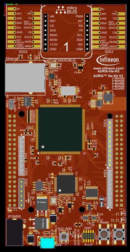
Copyright © Infineon Technologies AG 2021. All rights reserved.Hardware setup
This code example has been developed
for the board KIT_A2G_TC375_LITE.
In this example, the pin AN0, connected
to the board’s potentiometer, is used.
Note: The channels can be HW filtered by the
board, depending on which capacitor/resistors
couples are soldered. Consult the AURIX™
TC375 lite Kit’s User Manual to check which
channels are filtered by HW.
Note: The reference voltage (VAREF) of the
EVADC on the board KIT_A2G_TC375_LITE
is 3.3 V.
Copyright © Infineon Technologies AG 2021. All rights reserved.Implementation
Configure the CCU6 unit
Configuration of the CCU6 Timer is done in the init_CCU6() function by initializing an instance of the
IfxCcu6_Timer_Config structure, which contains the following fields:
› timer – a parameter that allows to choose which of the two timers to configure. In this case, T13 is the
master Timer and T12 is used as slave for its trigger.
› base – a structure that allows to set:
– t12frequency – input clock frequency in Hz of the Timer T12
– waitingTime – 16-bit register that determines the maximum count value for the Timer T12. It is used
as value for the period register, which represents the waiting time in ticks before a new trigger event
occurs for Timer T13
– t13frequency – input clock frequency in Hz of the Timer T13
– t13period – 16-bit register that determines the maximum count value for the Timer T13
› trigger – a structure for configuring the triggers for both timers
– t13InSyncWithT12 – allows synchronous operations between the two timers
› timer13 – a structure that allows to:
– t12SyncEvent – set the Timer T12 event that represents the Timer T13 trigger
– t12SyncDirection – define if a trigger event is to be considered valid based on the counting direction
of the Timer T12
Copyright © Infineon Technologies AG 2021. All rights reserved.Implementation
The functions used for CCU6 configuration are:
› IfxCcu6_Timer_initModuleConfig() – fills the configuration structure with default values
› IfxCcu6_Timer_initModule() – initializes the timer module with the user configuration
› IfxCcu6_enableInterrupt() and IfxCcu6_routeInterruptNode() – indicate which event generates the
Interrupt Service Request and on which Service Request line. This enables the CCU6 to trigger an ADC
conversion without the CPU intervention
› IfxCcu6_enableSingleShotMode() – configures the timer to count in single shot mode
› IfxCcu6_Timer_start() – starts the timer
The above functions can be found in the iLLD headers IfxCcu6_Timer.h and IfxCcu6.h.
Copyright © Infineon Technologies AG 2021. All rights reserved.Implementation
Timer module frequency
In Timer Mode, the input clock of the timer module is derived from the internal module clock fCC6.
By default, the internal module clock fCC6 is initialized by the iLLDs to run at 100 MHz.
Starting from this value, it is possible to set the timer module frequency to the following exact values:
100000000 Hz = 100 MHz ( fCC6 )
50000000 Hz = 50 MHz ( fCC6 / 2 )
25000000 Hz = 25 MHz ( fCC6 / 4 )
12500000 Hz = 12.5 MHz ( fCC6 / 8 )
6250000 Hz = 6.25 MHz ( fCC6 / 16 )
3125000 Hz ~ 3 MHz ( fCC6 / 32 )
1562500 Hz ~ 1.5 MHz ( fCC6 / 64 )
781250 Hz ~ 780 KHz ( fCC6 / 128 )
390625 Hz ~ 390 KHz ( fCC6 / 256 )
195312.5 Hz ~ 200 KHz ( fCC6 / 512 )
97656.25 Hz ~ 100 KHz ( fCC6 / 1024 )
48828.12 Hz ~ 50 KHz ( fCC6 / 2048 )
24414.06 Hz ~ 25 KHz ( fCC6 / 4096 )
12207.03 Hz ~ 12.5 KHz ( fCC6 / 8192 )
6103.51 Hz ~ 6 KHz ( fCC6 / 16384 )
3051.75 Hz ~ 3 KHz ( fCC6 / 32768 )
Note: Any value can be set as frequency parameter, but the software will round up the chosen value to the
nearest higher frequency listed in the above table (e.g. setting timerConfig.base.t12Frequency = 400000
the timer will run at 781250 Hz).
Copyright © Infineon Technologies AG 2021. All rights reserved.Implementation
Period Match Frequency calculation
To calculate the actual Period Match frequency fPM (the number of occurrences per second in which the timer
counter value reaches the period value and is reset), two parameters have to be considered: Timer clock
frequency and its period.
› The Timer clock frequency can be freely selected as described in the previous slide
› The period value is stored in a 16-bit register, which limits its maximum value to 65535
The Period Match frequency and period can then be calculated as:
fPM = (Timer clock frequency) / (period + 1)
TPM = (period + 1) / (Timer clock frequency)
In this example, a clock frequency equal to 48828 Hz is chosen for both timers, while the periods are set to
have a T12 period match frequency equal to 1 Hz (ADC sample rate, 1 sample/sec) and a T13 period match
(delay) time equal to 0.5 seconds (ADC sample delay).
Copyright © Infineon Technologies AG 2021. All rights reserved.Implementation
Configuration of the EVADC
The configuration of the EVADC is done in the init_EVADC() function in three different steps:
› Configuration of the EVADC module
› Configuration of the EVADC group
› Configuration of the EVADC channel
Configuration of the EVADC module
The functions used for configuring the EVADC module are:
› IfxEvadc_Adc_initModuleConfig() – initializes the EVADC module configuration structure with the
default values
› IfxEvadc_Adc_initModule() – initializes the EVADC module with the user configuration, which in this
case is the default configuration
Copyright © Infineon Technologies AG 2021. All rights reserved.Implementation
Configuration of the EVADC group
Configuration of the EVADC group is done by initializing an instance of the IfxEvadc_Adc_GroupConfig
structure, which contains the following fields:
› arbiter – a structure that represents the enabled request sources, which can be one of the three queue
sources. In this example, arbiter.requestSlotQueue0Enabled is set to TRUE, thus enabling the request
queue 0.
› queueRequest[0] – a structure that allows to configure the queue request source 0 by setting:
– triggerConfig – a parameter that specifies the trigger configuration
› master – to indicate which converter is the master
› groupId – to select which converter to configure
The functions used for configuring the EVADC group are:
› IfxEvadc_Adc_initGroupConfig() – fills the group configuration structure with default values
› IfxEvadc_Adc_initGroup() – initializes the EVADC group specified in the parameters with the user
configuration
Copyright © Infineon Technologies AG 2021. All rights reserved.Implementation
Configuration of the EVADC channel
Configuration of the EVADC channel is done by initializing an instance of the IfxEvadc_Adc_ChannelConfig
structure, which contains the following fields:
› channelId – a parameter that allows to choose which of the channels to configure
› resultRegister – indicates the register where the sample value is stored
› resultPriority – the priority of the result trigger interrupt
› resultServProvider – interrupt service provider for the result trigger interrupt. This can be any of the
available CPUs or the DMA. In this example, the interrupt is used to print the measurements through
UART communication
The functions used for configuring the EVADC channel are:
› IfxEvadc_Adc_initChannelConfig() – fills the channel configuration structure with default values
› IfxEvadc_Adc_initChannel() – initializes the channel with the user configuration
› IfxEvadc_Adc_addToQueue() – add the channel to the queue
When both the CCU6 and EVADC modules are configured, a single scan sequence is triggered by the CCU6
timer T13 period match event.
All the functions used for configuring the EVADC module, group and channel can be found in the iLLD header
IfxEvadc_Adc.h.
Copyright © Infineon Technologies AG 2021. All rights reserved.Implementation
Events timing
The graph shows the temporal evolution of events: T12 period matches, T13 period matches and ADC
sampling instants.
Copyright © Infineon Technologies AG 2021. All rights reserved.Implementation
Configuration of the UART
In this example, the UART connection is used to make the debugging more convenient and easier to
understand.
The init_UART() function initializes the UART communication.
The iLLD function IfxAsclin_Asc_initModuleConfig() fills the configuration structure ascConf with
the default values. Then, the parameters used to configure the module are set, depending on the
needed connection: baudrate, sampling mode, interrupts, Tx and Rx buffers and port pins
configuration.
Finally, IfxAsclin_Asc_initModule() initializes the module with the user configuration and
IfxAsclin_Asc_stdIfDPipeInit() initializes the standard interface to use the ASC module.
The above functions can be found in the iLLD header IfxAsclin_Asc.h.
Copyright © Infineon Technologies AG 2021. All rights reserved.Run and Test
› For this training, a serial monitor is required for visualizing the values. The monitor can be
opened inside the AURIX™ Development Studio using the following icon:
› The serial monitor must be configured with
the following parameters to enable the
communication between the board and the
PC:
– Speed (baud): 115200
– Data bits: 8
– Stop bit: 1
Copyright © Infineon Technologies AG 2021. All rights reserved.Run and Test
After code compilation and flashing the device, perform the following steps:
› Connect the board to the PC
› Open the serial monitor with the appropriate COM port and settings (can be seen
in the Device Manager)
› Check the ADC conversions sampled every one second in the serial monitor
console
Copyright © Infineon Technologies AG 2021. All rights reserved.References
› AURIX™ Development Studio is available online:
› https://www.infineon.com/aurixdevelopmentstudio
› Use the „Import...“ function to get access to more code examples.
› More code examples can be found on the GIT repository:
› https://github.com/Infineon/AURIX_code_examples
› For additional trainings, visit our webpage:
› https://www.infineon.com/aurix-expert-training
› For questions and support, use the AURIX™ Forum:
› https://www.infineonforums.com/forums/13-Aurix-Forum
Copyright © Infineon Technologies AG 2021. All rights reserved.Trademarks
All referenced product or service names and trademarks are the property of their respective owners.
Edition 2021-03 IMPORTANT NOTICE For further information on the product,
Published by The information given in this document shall in no technology, delivery terms and conditions and
Infineon Technologies AG event be regarded as a guarantee of conditions or prices please contact your nearest Infineon
81726 Munich, Germany characteristics (“Beschaffenheitsgarantie”) . Technologies office (www.infineon.com).
With respect to any examples, hints or any typical
© 2021 Infineon Technologies AG. WARNINGS
values stated herein and/or any information
All Rights Reserved. Due to technical requirements products may
regarding the application of the product, Infineon
contain dangerous substances. For information
Technologies hereby disclaims any and all
Do you have a question about this on the types in question please contact your
warranties and liabilities of any kind, including
document? nearest Infineon Technologies office.
without limitation warranties of non-infringement
Email: erratum@infineon.com
of intellectual property rights of any third party. Except as otherwise explicitly approved by
Infineon Technologies in a written document
Document reference In addition, any information given in this
signed by authorized representatives of Infineon
CCU6_ADC_1_KIT_TC375_LK document is subject to customer’s compliance
Technologies, Infineon Technologies’ products
with its obligations stated in this document and
may not be used in any applications where a
any applicable legal requirements, norms and
failure of the product or any consequences of the
standards concerning customer’s products and
use thereof can reasonably be expected to result
any use of the product of Infineon Technologies in
in personal injury.
customer’s applications.
The data contained in this document is exclusively
intended for technically trained staff. It is the
responsibility of customer’s technical
departments to evaluate the suitability of the
product for the intended application and the
completeness of the product information given in
this document with respect to such application.You can also read