Design and Implementation of SOC in NIOS-II Soft Core Processor for Secured Wireless Communication
←
→
Page content transcription
If your browser does not render page correctly, please read the page content below
International Journal of Computer Applications (0975 – 8887)
                                                                                            Volume 53– No.14, September 2012

  Design and Implementation of SOC in NIOS-II Soft Core
     Processor for Secured Wireless Communication
                  R.Ramachandran                                            J. Thomas Joseph Prakash
   Research Scholar, Manonmaniam Sundaranar                                   H.H. The Rajah’s College
     University, Tirunelveli, Tamilnadu, India.                         Pudukkottai – 622001, Tamilnadu, India

ABSTRACT                                                          implemented. There are plenty of methods can be used to
                                                                  encrypt data packets, all of which can easily be implemented
In the modern world, the information that could benefit the       through software, but not so easily decrypted when either the
individual / a group also can be used against such individual     original or its encrypted data stream are unavailable. (When
or group. Encryption is the technique of converting a plaintext   both source and encrypted data are available, code-breaking
(original data packet) into cipher text (encrypted message)       becomes much simpler, though it is not necessarily easy). The
which can be decoded back into the original message. There        best encryption methods have little effect on system
are several types of data encryptions schemes available which     performance (Slowing the system), and may contain other
form the basis of network security. Our proposed work deals       benefits such as data compression [4]. We have used the data
with the security based wireless communication system, with       encryption technique to implement the secured data
the NIOS-II soft core processor. Security in wireless             transmission and reception with NIOS-II soft core processor
communication is most essential, especially where hacking         [5]. It is having many features such as RISC (Reduced
and tampering are threats of the data packet. Hence               Instruction Set Computer) architecture, 32 bit processor, and
introduction of suitable security bits (Key) with the actual      its architecture consist of separate instruction and data bus
data packet is most important aspect in wireless                  (Harvard architecture). The SOPC ( System on programmable
communication to avoid such threats. It is really a significant   chip) builder is a tool used in conjunction with the Quartus II
and interesting area for the researcher. In this work, the data   CAD tool Software [6]. It allows the designer to easily create
encryption standard technique is used for the safety              a system based on the NIOS II processor, by selecting the
transmission and reception, and implemented it successfully       desired functional units and specifying their parameters. The
with the NIOS-II soft core processor.                             NIOS II processor is a configurable soft core processor.
                                                                  Configurable means that can be added or removed any
Keywords                                                          features or resources of the processor on the basis of
Wireless communication, NIOS-II soft core processor, FPGA,        performance or cost wise. Soft core means the processor core
SOC, Data Encryption.                                             is not fixed in silicon chip, but can be targeted to any Altera
                                                                  FPGA family.
1. INTRODUCTION                                                   This paper is organized as 1. Overview, 2. Implementation, 3.
In recent years, the wireless communication plays a vital role    Result and analysis, and 4. Conclusion.
in industries, home and government departments [1]. It is the
emerging field in electronic communication. One example of
                                                                  2. OVERVIEW
its growth is cellular systems. Cellular systems have             Our approach to achieve the aim of the proposed work is
experienced high growth over the last decade. Wireless            based on Altera NIOS II embedded soft core processor that
networks currently replace wired networks in many homes,          provides a highly configurable device and having excellent
companies and other campuses. Many new applications,              versatility. We have used Altera Cyclone Field Programmable
including smart homes, wireless sensor networks, automated        Gate Array (FPGA) and its peripherals to make the design to
factories and high ways, and remote telemedicine, are             be constructive. A well known Data Encryption Standard
emerging from research ideas into concrete systems [2].           (DES) Algorithm[7] is chosen for Encryption for secured data
Although the wireless communication is having numerous            transmission. The evaluation results obtained from the
applications, hacking and tampering the data packet are also      experiment are shown for analysis and verification of our
quite common. There are plenty of techniques of hacking the       design. The figure (1) shows block diagram of the proposed
data; especially in wireless communication is underway.           work. Referring the block diagram, the functional modules are
Such hacking methods [3] are; 1. Diverse hacker attack            1. Various Wireless sensor outputs, usually analog signals
methods, 2. Social Engineering, 3. Social spying, 4. Sniffing     (The Electrical output), 2. A/D converter, 3. Cyclone II
and more. In order to avoid hackings and tampering the data       FPGA, 4. GSM modem.
packets a suitable encryption technique has to be

                                                                                                                               1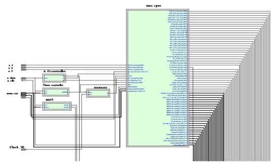
International Journal of Computer Applications (0975 – 8887)
Volume 53– No.14, September 2012
Sensor 1
GSM
A/D Cyclone II FPGA Module
Conversion
Sensor2 EP 2C35672C6
Sensor 3
Figure (1) – Block diagram of the proposed work
2.1 Analog to Digital Converter memory such as 8 MB SDRAM, 512 KB SRAM are also
available. Hence, DE2 development board is much suitable
platform for running NIOS II soft core processor. The figure
Analog to Digital converter [8] is configured with processor is (2) shows Altera’s DE2 development board.
8- bit converter, compatible with ADC 0809. The 8- channel
(Inputs IN0 to IN7) multiplexer can directly access any of 8-
single ended analog signals to be transmitted with the set of
address lines A,B,C. The clock chosen for conversion
600Khz.. The ADC 809 also having many desirable features,
such as no zero or full scale adjust required, and 0V to 5V
input range with single 5V power supply.
2.2 NIOS Embedded processor
The NIOS II Embedded processor is a general purpose
configurable Soft core processor [9,10]. In practice, most
FPGA designs implement some extra logic in addition to the
processor system. The processor could be virtually realized 2.4 RS-232 Serial Interface
on any of an Altera FPGA by using a System On a
Programmable Chip (SOPC) builder. NIOS II embedded
processor is having, Custom instructions; means Nios II An RS-232 interface [12] has many characteristics, 2. It
instructions, user-defined instructions accept values from up allows bidirectional full-duplex communication, 3. It can
to two 32-bit source registers and optionally write back a communicate at a maximum speed, at the rate of 10KBytes/s.
result to a 32-bit destination register. Nios II families are 1. Three are important pins for communication, they are RxD (
NIOS II/f (fast), 2. NIOS II/s (standard), and 3. NIOS II/e Receive Data- Pin No. 2), TxD ( Transmit Data- Pin No.3)
(economy). Any one of these can be used for design, depends and GND (Ground pin No. 5).
on the requirement.
2.4.1 Serial communication
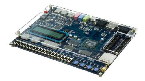
2.3 DE2 development board
Data is sent on bit by bit basis, that is one bit at a time; a
single wire is used for each direction. Since computers usually
DE2 development board consists of Cyclone II need at least several bits of data, the data is "serialized" before
EP2C35F672C6 with EPCS16 16-Mbit serial configuration being sent. Data is commonly sent by chunks of 8 bits. The
device, and many standard peripherals. It provides a high LSB (data bit 0) is sent first, the MSB (bit 7) last.
performance, low cost design with modern Altera devices and
tools. With Quartus II CAD tool, the designer can develop 2.4.2 Asynchronous communication
hardware design using HDLs in the on board FPGA. A set of
This interface uses an "asynchronous" protocol. In
asynchronous data transfer, handshake signals are used for
testing the readiness of the receiver. In our case the RS232 is
2International Journal of Computer Applications (0975 – 8887)
Volume 53– No.14, September 2012
function in the mode. In this mode of transmission, the speed 3. IMPLEMENTATION
and format has to decided before start the transmission. The
TxD line sends logic “1” as long as the line is idle. The start
bit (logic “0”) to be send before each byte of transmission. For transferring secured data transmission through wireless,
After the "start", data comes in the agreed speed and format, we have designed NIOS II processor with necessary
so the receiver can interpret it. The stop bit is usually logic peripheral interface. The entire implementation process is thus
“0”. assigned to two stages; 1. Hardware implementation, and 2.
Software Implementation.
The common baud rates of RS 232 Serial interface are
1200,9600,38400, and 115200. The speed can be easily 3.1 Hardware Implementation
calculated as, for example if the baud rate is 115200. T =
1/115200 = 8.7µs. If 8-bits data to be transmitted, that lasts 8 In Our design, we have effectively utilized the resources
x 8.7µs = 69µs. But in the Asynchronous format of available in the Altera NIOS II embedded processor
transmission, each byte requires an extra start and stop bit, so technology. In the laboratory we have taken the analog data
actually need of 10 x 8.7µs = 87µs. That translates to a which is then successfully converted to equivalent binary bits.
maximum speed of 11.5KBytes per second. These are the output bits of the ADC, which is 64- bit known
as plain text. With these binary bits (Plain text), C++ program
2.5 SIM 300 GSM modem was executed in the NIOS II processor on DE2 development
The figure (3) shows SIM 300 GSM modem. A GSM modem board to get the cipher text for secured data transmission, and
exposes an interface that allows applications such as then the cipher text was transmitted serially with RS 232
NowSMS to send and receive messages over the modem serial interface to the SIM 300, for transmitting the secured
interface. data (Cipher text) over the space. At another end the cipher
text was received successfully with another SIM 300, and then
the cipher text was deciphered. Since this process of
communication is purely asynchronous, the excellent
configurable and programmable properties of the NIOS II
processor enable us to simply implement the encryption and
decryption process on a single DE2 development board
significantly reducing the cost of the platform. The core of the
DE2 development board consists of Cyclone II
EP2C35F672C6 with EPCS16 16- Mbit serial configuration
device. The basic peripherals chosen are UART controller,
A/D controller, On chip memory, I/O controller, and a timer
in SOPC builder for the lowest Logic Elements (Les)
consumption. The figure (4) Shows how the NIOS II soft core
Figure (3) - SIM 300 GSM modem processor with the necessary peripherals are implemented in
FPGA. The completed SOPC design is then downloaded via
AT commands are instructions used to control a modem. AT JTAG UART to DE2 Board.
is the abbreviation of ATtention. Every command line starts
with "AT" or "at". That's why modem commands are called
AT commands. Many of the commands that are used to
control wired dial-up modems, such as ATD (Dial), ATA
(Answer), ATH (Hook control) and ATO (Return to online
ON Chip
data state), are also supported by GSM/GPRS modems and UART
Memory
mobile phones. Controller
2.6 Data Encryption Standard Algorithm NIOS II
CPU
I/O
Data Encryption Standard Algorithm is chosen to achieve a A/D
Controller
Converter
good secured data transmission [14,15]. The implementation
of this algorithm has been done with C++ language. A DES
key consists of 64 binary digits of which 56 bits are randomly
generated and used directly by the algorithm. In this
technique, data can be recovered from cipher (Encrypted
output) only by using exactly the same key used to encipher it. Cyclone II FPGA
Figure (4) - NIOS II CPU implementation on FPGA
Unauthorized recipients of the cipher who know the algorithm
but do not have the correct key cannot derive the original data
algorithmically. It is also possible to retrieve the original data Figure (4) - NIOS II CPU implementation on FPGA
by deciphering the text with original key and algorithm. A
standard algorithm based on a secure key thus provides a basis
for exchanging encrypted computer data by issuing the key
used to encipher it those authorized to have the data. The
security level has been proven to be competent for efficiently
defending the linear and differential cryptanalysis. The
characteristics of this algorithm make it appealing security
scheme for our proposed work.
3International Journal of Computer Applications (0975 – 8887)
Volume 53– No.14, September 2012
3.2 Software Implementation (L1, R1) = (R0, L0 ^ f(R0, k1))
(L2, R2) = (R1, L1 ^ f(R1, k2))
Having built up the hardware, the Data Encryption Standard
(DES) algorithm needs to be programmed in software. The ......
software development environment of NIOS II processor that
called NIOS II Integrated Development Environment (IDE) is C' = (R16, L16), swapping the two parts
based on the C/ C++ compiler. The program was written in
C++, and the specifications of DES carefully coded with C = FP(C'), applying final permutation
suitable parameters.
where ^ is the XOR operation.
The algorithm is designed to encipher and decipher blocks of
data consisting of 64 bits under control of a 64- bit key ( the
1. The round function f(R,k) is defined as:
left most bit of a block is bit number one). Deciphering must
be accomplished by using the same key as for enciphering,
but with the schedule of addressing the key bits altered so that Input:
the deciphering process is the reverse of the enciphering
process. A block to be enciphered is subjected to initial R: 32-bit input data
permutation IP, then to a complex key-dependent k: 48-bit round key
computation and finally to a permutation which is the inverse E: Expansion permutation
of the initial permutation IP-1. The key-dependent P: Round permutation
computation can be simply defined in terms of a function f, s(): S boxes function
called the cipher function, and a function KS, called the key
schedule. The figure (5) shows the illustration details of the Output
DES.
R' = f(R,k): 32-bit output data
DES algorithm Algorithm
X = E(R), applying expansion permutation and returning 48-
bit data
X' = X ^ k, XOR with the round key
X" = s(X'), applying S boxes function and returning 32-bit
data
R' = P(X"), applying the round permutation
2. The S boxes function s(X) is defined as:
Input:
X: 48-bit input data
S1, S2, ..., S8: 8 S boxes - 4 x 16 tables
Output:
Figure (5) – DES illustration X' = s(X): 32-bit output data
Algorithm:
Input:
(X1, X2, ..., X8) = X, dividing X into 8 6-bit parts
T: 64 bits of clear text X' = (S1(X1), S2(X2), ..., S8(X8))
k1, k2, ..., k16: 16 round keys where Si(Xi) is the value at row r and column c of S box i
IP: Initial permutation with
FP: Final permutation r = 2*b1 + b6
f(): Round function c = 8*b2 + 4*b3 + 2*b3 + b4
b1, b2, b3, b4, b5, b6 are the 6 bits of the Xi
Output:
4. RESULT AND ANALYSIS
C: 64 bits of cipher text
In this work, the designed System on chip (SOC) on NIOS- II
Algorithm: processor successfully implemented. The resultant hardware
configuration implemented, as shown in the figure (6) as
T' = IP(T), applying initial permutation follows.
(L0, R0) = T', dividing T' into two 32-bit parts
4International Journal of Computer Applications (0975 – 8887)
Volume 53– No.14, September 2012
5. CONCLUSION
Based on our proposed work hardware implementation
platform, we suggest a novel methodology for transmitting
wireless data. This method takes into account the level of
security, execution speed, memory usage and power
consumption altogether, all of which are desired properties for
wireless data transmission. With the comprehensive
consideration of all these factors for certain application in
wireless communication could be found with high efficiency
and low cost. This paper has proposed a comprehensive
approach of secured data transmission in wireless
communication, and the feasibility of the design has been
studied. Certain questions are to be answered in terms of
speed in the future study.
REFERENCES
[1] David Tse, Pramod Viswanath, Fundamentals of
Wireless Communication 2005
[2] Andrea Goldsmith, Wireless communication
[3] Cyrus Peikari, Seth Fogie, Wireless Maximum Security,
Chapter 6, Sams publishing, 2003.
Figure (6)- RTL View of the NIOS II processor [4] H.Chen, A.Perrig.” Security and privacy in Sensor
implementation Networks” Computer, Vol. 36, Issue 10, Oct. 2003, pp
103-105.
Test conducted on the prototype work by giving the analog
[5] Nios II processor Reference handbook,
data (Thermistor output) and transmitted successfully with
http://www.altera.com/
encryption through GSM modem SIM 300. Also we have
received appropriate message as output. The NIOS II/e ( [6] http://users.ece.gatech.edu/~hamblen/DE1/DE1_CDRO
economy core) is designed to minimize the cost of the design. M/DE1_tutorials/tut_sopc_introduction_verilogDE2.pdf.
In this work, the total logic elements consumed only 20%,
total logic functions are used only 17%. Other parameters are [7] Federal Information Processing Standards Publication
used in the work as shown in the table (1). 46-3, 1999 October 25.
[8] Data sheet of National Semiconductor,
Family Cyclone II www.national.com
Device EP2C35F672C6 [9] Altera NIOS II Software Developer’s Handbook,
http://www.altera.com/
Total Logic elements 6,574 / 33,216 (20%) [10] Altera Quartus II Handbook, http://www.altera.com/
Total combinational 5,557 / 33,216 (17%) [11] DE2 Development and Education Board,
functions http://www.altera.com/
[12] RS 232 Serial interface,
Dedicated Logic registers 3,524 /33,216 (11%)
http://www.fpga4fun.com/SerialInterface1.html
Total registers 3641 [13] http://en.wikipedia.org/wiki/Subscriber_Identity_Module
.
Total pins 429 /475 (90%)
[14] Alfred Menezes, Paul van Oorschot , Scott Vanstone,
Handbook of Applied Cryptography.
Total virtual pins 0
[15] Jonathan Katz , Yehuda Lindell, Introduction to Modern
Total memory bits 387,584/483,840 (80%) Cryptography: Principles and Protocols (Chapman &
Hall/CRC Cryptography and Network Security Series).
Embedded multiplier 9-bits 4/70 (6%)
Total PLLs 2/4 (50%)
Table (1) - consumption details of NIOS II core processor
5You can also read