DigitalCommons@USU Utah State University
←
→
Page content transcription
If your browser does not render page correctly, please read the page content below
Utah State University
DigitalCommons@USU

All Graduate Theses and Dissertations                                              Graduate Studies

8-2020

Design of a Sweeping Impedance Probe for the SPORT Mission
Caleb W. Young
Utah State University

Follow this and additional works at: https://digitalcommons.usu.edu/etd

   Part of the Systems and Communications Commons

Recommended Citation
Young, Caleb W., "Design of a Sweeping Impedance Probe for the SPORT Mission" (2020). All Graduate
Theses and Dissertations. 7884.
https://digitalcommons.usu.edu/etd/7884

This Thesis is brought to you for free and open access by
the Graduate Studies at DigitalCommons@USU. It has
been accepted for inclusion in All Graduate Theses and
Dissertations by an authorized administrator of
DigitalCommons@USU. For more information, please
contact digitalcommons@usu.edu.
DESIGN OF A SWEEPING IMPEDANCE PROBE FOR THE SPORT MISSION

                                          by

                                  Caleb W. Young

                       A thesis submitted in partial fulfillment
                          of the requirements for the degree

                                          of

                              MASTER OF SCIENCE

                                          in

                                Electrical Engineering

Approved:

Charles M. Swenson, Ph.D.                  Jonathan D. Phillips, Ph.D.
Major Professor                            Committee Member

Jacob Gunther, Ph.D.                       Janis L. Boettinger, Ph.D.
Committee Member                           Acting Vice Provost of Graduate Studies

                            UTAH STATE UNIVERSITY
                                  Logan, Utah

                                         2020
ii
Copyright c Caleb W. Young 2020
All Rights Reservediii
ABSTRACT
Design of a Sweeping Impedance Probe for the SPORT Mission
by
Caleb W. Young, Master of Science
Utah State University, 2020
Major Professor: Charles M. Swenson, Ph.D.
Department: Electrical and Computer Engineering
In our modern world satellite systems are an evermore common part of day to day life.
Reliable communication from the ground to these satellites is becoming more and more
necessary. Plasma scintillations in the ionosphere can make these communications difficult
or even impossible. By gaining a better understanding of these scintillations, times of bad
satellite connection can be predicted in the same way terrestrial weather gets predicted
and reported today. The objective of the SPORT mission is to gain a better understand-
ing of these plasma scintillations. In order to measure plasma density, and gain a better
understanding of plasma scintillations, a Sweeping Impedance Probe (SIP) can be used.
It is proposed that the SIP for the SPORT mission be a digital rework of a probe used
on the ASSP mission. By using digital processing methods instead of analog methods the
new probe can be more accurate in the plasma measurement.
This thesis will describe the theory and design of the SPORT SIP and its advantages
over previous analog methods. The design is detailed for both the analog and digital portions
of the probe along with a selection of testing data. Potential changes are also discussed.
(67 pages)iv
PUBLIC ABSTRACT
Design of a Sweeping Impedance Probe for the SPORT Mission
Caleb W. Young
In our modern world satellite systems are an evermore common part of day to day life.
Reliable communication from the ground to these satellites is becoming more and more
necessary. Plasma scintillations in the ionosphere can make these communications difficult
or even impossible. By gaining a better understanding of these scintillations, times of bad
satellite connection can be predicted in the same way terrestrial weather gets predicted
and reported today. The objective of the SPORT mission is to gain a better understand-
ing of these plasma scintillations. In order to measure plasma density, and gain a better
understanding of plasma scintillations, a Sweeping Impedance Probe (SIP) can be used.
It is proposed that the SIP for the SPORT mission be a digital rework of a probe used
on the ASSP mission. By using digital processing methods instead of analog methods the
new probe can be more accurate in the plasma measurement.
This thesis will describe the theory and design of the SPORT SIP and its advantages
over previous analog methods. The design is detailed for both the analog and digital portions
of the probe along with a selection of testing data. Potential changes are also discussed.v
ACKNOWLEDGMENTS
First off I need to thank Dr. Swenson. His guidance as I have worked through my
entire masters program and this project has been invaluable. Just being able to work on
the SPORT project was probably the most important part of all of my time at school. My
abilities as an engineer would not be anywhere near what they are now without this chance
to gain experience on a real project. So much that I and the other students learned came
from the time that Dr. Swenson was able to give us in his endlessly busy schedule.
I also need to thank all the other students that were involved on this project. Nathan
Tipton and Jordan Haws and I starting down this road the same day. We worked on all
of the instruments, not just the impedance probe. Without them there is no impedance
probe, no USU space weather instrument for that matter. So much of both the digital and
analog design was from working with Nathan. Many a bug would have been much harder
to smash if it weren’t for his help. Make sure to check out his thesis on the Langmuir Probe
when it gets published. I wish I had a reason to cite it in here.
Then there is Russell Babb, Joel Mork, Dr. Phillips, Lucas Anderson, our friends in
Brazil, and Colton Anderson who made my time at the CSE as enjoyable as it was. They
all had a hand in what is now a functional set of probes.
And, of course, my wife Emily. Without her this thesis probably wouldn’t have gotten
finished.
Caleb Youngvi
CONTENTS
Page
ABSTRACT . . . . . . . . . . . . . . . . . . . . . . . . . . . . . . . . . . . . . . . . . . . . . . . . . . . . . . iii
PUBLIC ABSTRACT . . . . . . . . . . . . . . . . . . . . . . . . . . . . . . . . . . . . . . . . . . . . . . . iv
ACKNOWLEDGMENTS . . . . . . . . . . . . . . . . . . . . . . . . . . . . . . . . . . . . . . . . . . . . v
LIST OF TABLES . . . . . . . . . . . . . . . . . . . . . . . . . . . . . . . . . . . . . . . . . . . . . . . . . viii
LIST OF FIGURES . . . . . . . . . . . . . . . . . . . . . . . . . . . . . . . . . . . . . . . . . . . . . . . . ix
ACRONYMS . . . . . . . . . . . . . . . . . . . . . . . . . . . . . . . . . . . . . . . . . . . . . . . . . . . . . xi
1 INTRODUCTION . . . . . . . . . . . . . . . . . . . . .... ..... .... .... . .... ..... 1
1.1 The SPORT Mission . . . . . . . . . . . . . . . . . . . . . . . . . . . . . . . 2
1.2 The SPORT Impedance Probe . . . . . . . . . . . . . . . . . . . . . . . . . 3
1.3 Literature Review . . . . . . . . . . . . . . . . . . . . . . . . . . . . . . . . 5
1.3.1 The ASSP Mission . . . . . . . . . . . . . . . . . . . . . . . . . . . . 5
1.4 Thesis Statement and Research Task . . . . . . . . . . . . . . . . . . . . . . 6
1.5 Thesis Outline . . . . . . . . . . . . . . . . . . . . . . . . . . . . . . . . . . 7
2 REQUIREMENTS AND THEORY OF OPERATIONS . . .... .... . .... ..... 8
2.1 SIP Theory of Operation . . . . . . . . . . . . . . . . . . . . . . . . . . . . . 8
2.1.1 Signals and Impedances . . . . . . . . . . . . . . . . . . . . . . . . . 8
2.2 Probe Model . . . . . . . . . . . . . . . . . . . . . . . . . . . . . . . . . . . 9
2.2.1 I/Q Sampling . . . . . . . . . . . . . . . . . . . . . . . . . . . . . . . 12
2.2.2 System Overview . . . . . . . . . . . . . . . . . . . . . . . . . . . . . 14
2.3 SPORT Mission Requirements . . . . . . . . . . . . . . . . . . . . . . . . . 15
2.4 Plasma Measurement Requirements . . . . . . . . . . . . . . . . . . . . . . 17
2.5 Sweep Function . . . . . . . . . . . . . . . . . . . . . . . . . . . . . . . . . . 17
2.6 Track Function . . . . . . . . . . . . . . . . . . . . . . . . . . . . . . . . . . 18
3 ANALOG SYSTEM DESIGN . . . . . . . . . . . . . . . . . . . . . . . . . . . . . . . . . . . . .. 19
3.1 Concept of Operations of the Sweeping Impedance Probe Analog System . 19
3.2 Source Generation . . . . . . . . . . . . . . . . . . . . . . . . . . . . . . . . 20
3.2.1 NCO Output and High-Speed DAC . . . . . . . . . . . . . . . . . . 21
3.2.2 Reconstruction Filter . . . . . . . . . . . . . . . . . . . . . . . . . . 22
3.3 Current Measurement . . . . . . . . . . . . . . . . . . . . . . . . . . . . . . 25
3.3.1 RF Head . . . . . . . . . . . . . . . . . . . . . . . . . . . . . . . . . 25
3.3.2 Sampling . . . . . . . . . . . . . . . . . . . . . . . . . . . . . . . . . 26vii
4 DIGITAL SYSTEM DESIGN . . . . . . . . .... .... . .... .... .... . .... . . . . . 28
4.1 Signal Generation . . . . . . . . . . . . . . . . . . . . . . . . . . . . . . . . . 29
4.2 Signal Reception and Processing . . . . . . . . . . . . . . . . . . . . . . . . 32
4.3 Sweep Control . . . . . . . . . . . . . . . . . . . . . . . . . . . . . . . . . . 33
4.4 Track Control . . . . . . . . . . . . . . . . . . . . . . . . . . . . . . . . . . . 33
4.5 Data Handling and Transmission . . . . . . . . . . . . . . . . . . . . . . . . 35
5 TESTING AND VERIFICATION . . . . . . . . . . . . . . . . .... .... . .... .... .. 38
5.1 Calibration Hardware . . . . . . . . . . . . . . . . . . . . . . . . . . . . . . 39
5.1.1 Frequency Output Testing . . . . . . . . . . . . . . . . . . . . . . . . 41
5.1.2 Precision, Gain, and Linearity Testing . . . . . . . . . . . . . . . . . 43
5.1.3 Frequency Response Testing . . . . . . . . . . . . . . . . . . . . . . . 43
5.1.4 Frequency Lock Testing . . . . . . . . . . . . . . . . . . . . . . . . . 48
5.2 Testing Conclusion . . . . . . . . . . . . . . . . . . . . . . . . . . . . . . . . 48
6 CONCLUSION . . . . . . . . . . . . . . . . . . . . . . . . . . . . . . . . . . . . . . . . . . . . . . . . . 50
6.1 Potential Changes . . . . . . . . . . . . . . . . . . . . . . . . . . . . . . . . 50
REFERENCES . . . . . . . . . . . . . . . . . . . . . . . . . . . . . . . . . . . . . . . . . . . . . . . . . . . 52
APPENDICES . . . . . . . . . . . . . . . . . . . . . . . . . . . . . . . . . . . . . . . . . . . . . . . . . . . . 54
A Included CD . . . . . . . . . . . . . . . . . . . . . . . . . . . . . . . . . . . . 55viii
LIST OF TABLES
Table Page
2.1 Top level requirements for the SPORT mission . . . . . . . . . . . . . . . . 16
2.2 Derived Requirements for the USU SIP . . . . . . . . . . . . . . . . . . . . 17
5.1 Testing needs to meet requirements . . . . . . . . . . . . . . . . . . . . . . . 38ix
LIST OF FIGURES
Figure Page
1.1 Top Level Diagram of the SPORT Space Weather Instrument . . . . . . . . 4
2.1 Example of the effects of impedance . . . . . . . . . . . . . . . . . . . . . . 10
2.2 Theoretical impedance characteristics for a cylindrical probe . . . . . . . . . 11
2.3 Block diagram of the mixing operation . . . . . . . . . . . . . . . . . . . . . 13
2.4 High level diagram of how the I/Q data will be generated . . . . . . . . . . 14
3.1 Conceptual diagram of the analog system . . . . . . . . . . . . . . . . . . . 20
3.2 Diagram of the Signal Generation chain for the SIP . . . . . . . . . . . . . . 21
3.3 Conceptual diagram of the reconstruction filter . . . . . . . . . . . . . . . . 22
3.4 Magnitude Response of the 7th order Elliptic Filter . . . . . . . . . . . . . . 23
3.5 Phase Response of the 7th order Elliptic Filter . . . . . . . . . . . . . . . . 23
3.6 Diagram of the RF Head circuit . . . . . . . . . . . . . . . . . . . . . . . . . 25
3.7 Schematic of Sampling System . . . . . . . . . . . . . . . . . . . . . . . . . 26
4.1 Top Level Diagram Digital System . . . . . . . . . . . . . . . . . . . . . . . 28
4.2 NCO and FS ADJ System . . . . . . . . . . . . . . . . . . . . . . . . . . . . 30
4.3 Signal Reception and Processing Chain . . . . . . . . . . . . . . . . . . . . . 32
4.4 Sweep Control System . . . . . . . . . . . . . . . . . . . . . . . . . . . . . . 33
4.5 Tracking Control Loop . . . . . . . . . . . . . . . . . . . . . . . . . . . . . . 34
4.6 Granule Structure of the SIP Sweep Packet . . . . . . . . . . . . . . . . . . 35
4.7 Granule Structure of the SIP Track Packet . . . . . . . . . . . . . . . . . . 36
4.8 Data Flow of the Data Packetization . . . . . . . . . . . . . . . . . . . . . . 36
5.1 Type 1 Calibrator . . . . . . . . . . . . . . . . . . . . . . . . . . . . . . . . 40x 5.2 Type 2 Calibrator . . . . . . . . . . . . . . . . . . . . . . . . . . . . . . . . 40 5.3 FFT of 10MHz Voltage Source . . . . . . . . . . . . . . . . . . . . . . . . . 42 5.4 FFT of 20MHz Voltage Source . . . . . . . . . . . . . . . . . . . . . . . . . 42 5.5 Response of Resistive Load . . . . . . . . . . . . . . . . . . . . . . . . . . . 44 5.6 Response of Capacitive Load . . . . . . . . . . . . . . . . . . . . . . . . . . 45 5.7 Response of Inductive Load . . . . . . . . . . . . . . . . . . . . . . . . . . . 46 5.8 Response of Tuned Load . . . . . . . . . . . . . . . . . . . . . . . . . . . . . 47 5.9 Sample of tracking data . . . . . . . . . . . . . . . . . . . . . . . . . . . . . 49
xi

                                 ACRONYMS

AC       Alternating Current
ADC      Analog-to-Digital Converter
ASSP     Auroral Spatial Structures Probe
CDS      Correlated Double Sampling
CORDIC   Coordinate Rotation Digital Computer
DAC      Digital-to-Analog Converter
DC       Direct Current
EFP      Electric Field Probe
FFT      Fast Fourier Transform
FIFO     First-In, First-Out
FPGA     Field Programmable Gate Array
GSFC     Goddard Space Flight Center
GPS      Global Positioning System
HSADC    High Speed Analog to Digital Converter
HSDAC    High Speed Digital to Analog Converter
HDL      Hardware Description Language
ITA      Instituto Tecnológico de Aeronáutica
LPF      Low-Pass Filter
LSB      Least Significant Bit
LUT      Look-Up Table
MSB      Most Significant Bit
MSFC     Marshall Space Flight Center
NASA     National Aeronautics and Space Administration
NCO      Numerically Controlled Oscillator
RF       Radio Frequency
R-L-C    Resistive Inductive Capacitive
RTL      Register-transfer Level
xii PID Proportional-Integral-Differential SIP Sweeping Impedance Probe SLP Sweeping Langmuir Probe SPORT Scintillation Prediction Observation Research Task USU Utah State University UTD University of Dallas Texas VHDL Very High Speed Integrated Circuit Hardware Description Language VNA Vector Network Analyzer
CHAPTER 1

                                    INTRODUCTION

    Our lives today are increasingly dependent on satellite systems. These systems provide

us services such as global imaging, global positioning, and television broadcasting. All are

incredibly useful services in our modern times. The main technology that makes these

services possible is the ability to consistently communicate from the earths surface to the

satellite. If that communication were to be removed, or just disrupted, these services would

be rendered unusable.

    One such disruption that causes scintillation on radio transmissions are plasma bubbles

that often occur at night in the equatorial region of the Earth’s ionosphere. The ionosphere

is a layer of the atmosphere that contains high levels of ionized particles, electrons and

ions, referred to as plasma. Under normal conditions, the ionosphere has little effect on the

passage of radio waves between the earth and the satellites above, because the ionospheric

plasma has a very uniform density. The bubbles are pockets of low-density plasma that rise

up from the bottom of the ionosphere into the higher density plasma above. When these

bubbles appear they produce turbulence in the ionospheric plasma density and the radio

waves passing through this turbulence become diffused and can be unusable. This effect

can be compared to light passing through water. When the water is still and calm the light

passes through with little change, but when there are bubbles present the light becomes

scattered and one cannot see through the water anymore. While the plasma bubbles and the

turbulence caused by their upward rise persist, satellite communications are often stopped

until the ionosphere returns to a calm state.

    Over areas of South America plasma bubbles are very common nightly occurrences,

posing troubles to industries that depend on satellite communications. For example, preci-

sion agriculture, which relies on GPS navigation, has to be stopped when a bubble forms in

the ionosphere above. For reasons such as this, being able to understand what triggers and
2
being able to predict these bubbles is of major interest to countries where plasma bubbles
are common.
The scientific community needs observations of the space environment before scientific
models can reasonably be developed to predict when bubbles will happen. Observations
are needed under all possible conditions including pre-bubble, post-bubble, and during a
bubble to understand what triggers bubble formation. The measurements to be made in
space by the Scintillation Prediction Observation Research Task (SPORT) spacecraft, along
with ground based radars and ionosondes, will provide the data need to develop and test
models to predict when these bubbles occur.
1.1 The SPORT Mission
The SPORT mission is a CubeSat mission that is geared toward learning and under-
standing more about what gives rise to these plasma bubbles and how scintillations are
caused by the ionosphere. The mission is a joint science mission between the United States
of America (USA) and Brazil. In the USA, Utah State University (USU), University of
Dallas Texas (UTD), Marshall Space Flight Center (MSFC), Goddard Space Flight Cen-
ter (GSFC), and The Aerospace Corporation are all organizations that will develop and
fly instruments and payloads to better understand the conditions that give rise to plasma
scintillations. In Brazil, the Instituto Teconològico de Aeronàutica (ITA) will be providing
the spacecraft, flight computer, while the Instituto Nacional de Pesquisas Espaciais (INPE)
will provide communication capabilities and telemetry handling from the ground through
their EMBRACE program.
The SPORT program was selected by NASA headquarters in December of 2016 to pro-
ceed and funding was made available to the US partners in the fall of 2017. Funding for the
Brazil portion of the program occurred in early 2018. The required U.S.-Brazil Framework
Agreement was ratified in April 2018 and NASAs Office of International and Interagency
worked with the U.S. Embassy in Brazil to press for conclusion of the Implementing Ar-
rangement in early 2019. Delivery of the completed US instruments to Brazil is expected
in the summer of 2020 with launch of the spacecraft in fall 2021.3
1.2 The SPORT Impedance Probe
Utah State University is providing a suite of three instruments for measuring plasma
density and temperature of the ionosphere. The USU payload will consist of two Electric
Field Probes (EFP), a Sweeping Langmuir Probe (SLP), and a Sweeping Impedance Probe
(SIP). This suite of instruments is referred to as the Space Weather Probes. Other smaller
measurement devices will also be included on the Space Weather Probes. A top level
diagram of the instrumentation for the Space Weather Probes is shown in Figure 1.1. Both
the SIP and the SLP will be used measure the ionospheric plasma density but with very
different techniques. Both probes measure the properties of a probe immersed in plasma,
but the SIP uses the AC impedance of the probe while the SLP uses the DC resistance to
determine the plasma density. An advantage of the SIP technique is that it can determine
absolute electron density, irrespective of the payload charging and surface contamination
by monitoring the changing impedance of the probe. The SLP is a technically simpler
probe to implement but can only reliably measure changes in plasma density and cannot be
calibrated to provide an absolute measurement without comparison to some other technique
such as the SIP. The impedance probe technique has been used for over fifty years to probe
the electron density in the Earths ionosphere on sounding rockets and spacecraft [1–3].
By using both the SLP and the SIP techniques together a more accurate plasma density
measurement can be achieved. The two probes will be used to check each other for proper
measurements and to provide a fallback for conditions under which one probe may not be
operating.
The SIP will be used to determine electron density by monitoring the current supplied
to a short monopole antenna when driven with a low-voltage RF signal. The probe length
(approx. 30 cm) is a fraction of the free space wave-length of the applied RF signals (1
– 30MHz) such that it has a capacitive impedance. To first order the impedance of the
probe is dependent on the average dielectric properties encompassed by the near fields that
exist between the probe and the spacecraft. Essentially, the probe and spacecraft form
a complex geometry capacitor that is filled with the ionospheric plasma. The theoretical4
8 7 6 5 4 3 2 1
SCIENCE INSTRUMENTATION
Fig. 1.1: Top Level Diagram of the SPORT Space Weather Instrument
S1 + IA
G=2 ADC PCB
EFP Probes
SC_Chassis - G=2
Electric INA116 150 Hz LPF 1 kHz LPF
MMCX (4)
G=0.5
Field 200 kS/s
D Probes D
S2 + IA Real-Time
G=2 G=2 ADC Magnetometer
SC_Chassis -
1 kHz LPF
Clock
150 Hz LPF
INA116
G=0.5
+
200 S/s
G=10 ADC
- 100kHz LPF
20 Hz HPF
INA129
20 kS/s
Microsemi Housekeeping
LP Sweep &
DAC SmartFusion2 Monitoring
+
Low
ADC
FPGA
Langmuir
Gain
Sweeping -
100kHz LPF Imax 50.16 µA .2nA/Count
Probe
INA129
MMCX
+
C
Langmuir LP
TA 200 kS/s C
Micro USB
-
Probe AD795
+
High
-30mV/uA Gain ADC Imax 50.01 nA .2pA/count Digital FTDI
-
INA129
100kHz LPF Isolators Programmer
Requirements:
Low Gain – 50µA at 18bits
High Gain – 50nA at 18bits 10 MS/s ARM µC
DAC
Ethernet
FSADJ
80 MS/s
DAC
30 MHz
Recons t
Impedance
Sweeping Antenna HS 40 MS/s
Isolated
Probe
Impedence G=52 ADC
Power System
Burden GNDA
B Probe Resistor B
GNDD
Imp Probe
Magnitude Pwr 4V_REF
ADC
Detect ±4.5V ±1.8V 5VA 1.8V_D 3.3V_D
Phase 200 kS/s
Flip Star Ground
COMP COMP ADC
Flop 2 kHz LPF Digital
Isolators
Chassis GND_SC GNDD GNDA
Legend
Omnetics Connector (21 Pin)
Analog Data Out PROGRAM
Center For Space Engineering
A SPI Packet GND_SIG VBATT VGND CSIP UTAH ST ATE UNIVERSITY COLLEGE OF ENGINEERING A
PPS ACK 5V_SC 3.3V_SC
Digital Data (4-wire) Ready (x7) (x2) (x2)
NEXT ASSY. TITLE
Logan, Utah 84322
N/A
Analog Data In TITLE
DESC RIPTION
N/A
Power
ENGINEER ITEM DWG N O. SHT REV
C. Swenson SPORT SLP EFP SIP DIAGRAMS REV -
LAST MOD IFIED FIL E N AME SHEET
Tuesday, August 6, 2019 5.VSDX 2 OF 15
8 7 6 5 4 3 2 15
impedance of such probes has been studied extensively [4–7] along with their use as a plasma
diagnostic [8–10]. A probe’s impedance can change by factors of 20 in magnitude and 180
degrees in phase from its free space values over nominal ionospheric density ranges. The
dielectric properties of the plasma modify the capacitive impedance of the probe into a
complex response characterized by two resonances. The lower frequency resonance has the
characteristics of a series R-L-C circuit resonance while the higher frequency has a parallel
R-L-C circuit characteristic. The series resonance occurs at the electron gyro frequency
modified by the capacitance of the plasma sheath surrounding the probe spacecraft system.
The parallel resonance occurs at the upper hybrid frequency which is determined by the
electron density and magnetic field magnitude.
1.3 Literature Review
The Sweeping Impedance Probe for the SPORT mission is primarily based on the design
implemented on the ASSP mission. The ASSP mission will be discussed and reviewed here.
1.3.1 The ASSP Mission
The Auroral Spatial Structures Probe (ASSP) was a NASA-sponsored sounding rocket
mission that was launched in early 2015. The sounding rocket was launched to study what
happens to the Earth’s electric and magnetic fields during an aurora [11]. The rocket
contained six sub-payloads that were ejected during flight and one main payload attached
to the rocket itself. Each payload included a Langmuir Probe, Magnetometer, Electric
Field Probe, and a GPS receiver. Additionally, the main payload also contained a modified
Langmuir Probe and an Impedance Probe [11, 12]. The design for the ASSP SIP was based
on designs for a Vector Network Analyzer (VNA). The operation of a VNA is to output
an AC signal to a device and calculate the magnitude and phase of the returning signal
compared to the original signal. The reference AC signal generation and the mixing to
find the real and imaginary components of returning signal were all done with dedicated
analog components. Only the processed signal components were sampled and then sent to
the ground [12].6
To increase the accuracy of the measurements, the ASSP impedance probe implemented
an oversampling method, referred to as Correlated Double Sampling (CDS). The signal from
the probe was mixed with two sets of sinusoidal signals, the usual cosine and negative sine
signals along with a sine and negative cosine (rotated 180 degrees from the original set).
This other set of signals rotates the mixed signal around the complex plane allowing for the
analog offset to be calculated and removed by finding the difference between the two mixed
signals. If there is no offset, when the secondary mixed signal is subtracted from the first
mixed signal the difference will come to zero because they are exactly opposite. If an offset
is present the difference between the two signals represents the offset [12].
The possible problem that this method presents is that the probe signals used for the
multiple mixing stages were received at different times and locations across the probe’s path
through space. By using signals from different times and locations a small amount of error
is added to the end measurement. This error is small compared to the errors removed by
performing CDS.
1.4 Thesis Statement and Research Task
It is proposed to implement the Sweeping Impedance Probe for the SPORT mission as
the research component for this Master of Science Degree. The Sweeping Impedance Probe
for the SPORT mission will use the in-phase and quadrature (I/Q) detection techniques
demonstrated on the ASSP mission. What differentiates the approach for the SIP on the
SPORT mission from the impedance probe on the ASSP mission is an increased emphasis
on digital signal processing on Field Programmable Gate Arrays (FPGAs) instead of using
dedicated analog hardware. The ASSP mission used an analog mixer to shift the measure-
ments at RF frequencies to baseband and to provide I and Q observations. Our proposed
approach for the SPORT mission will use a high-speed analog to digital converter to sample
the RF-signal and implement the mixing digitally in the FPGA. This digital mixing removes
the need for CDS that was used on the ASSP mission. The remaining analog components
of the ASSP instrument will be updated to reduce power consumption and decrease noise
within the SPORT SIP.7
Implementing more of the SIP using digital processing techniques instead of dedicated
analog hardware provides the following benefits. First, digital processing approach is less
susceptible to degradation and drift over time. Analog components may have characteristics
that change from the original calibration due the space environment or aging. Second,
digital processing is more flexible and can be changed to be mission specific without having
to make all new hardware. All that is needed to change the system is to reprogram the
digital components. This proposed shift to digital makes modifying the system for a future
mission a simpler task compared to an all analog system.
The thesis statement for the proposed research is: Can a miniature low-power sweeping
impedance probe be developed using a high speed analog to digital converter and digital
signal processing techniques that meets the SPORT mission science objectives?
1.5 Thesis Outline
The remainder of the thesis will be structured with the following chapters.
Chapter 2 will describe the design requirements that the SIP must meet to be considered
successful. This includes high level science requirements and how they were converted to
engineering requirements. How the system is designed from these requirements will be
discussed.
Chapter 3 will include details of the analog portion of the system. Designs of the analog
system will be presented along with reasoning for the design. The analog circuitry for the
RF signal handling and conditioning is described with schematic designs.
Chapter 4 discusses details of the design of the digital system. How the FPGA system
was designed and all the processing blocks will be shown. The data flow from single data
samples to processed data packets will be shown.
Chapter 5 will discuss the testing procedures to verify system functionality.
Chapter 6 will conclude and discuss future work and possible changes to the design.CHAPTER 2
REQUIREMENTS AND THEORY OF OPERATIONS
2.1 SIP Theory of Operation
The impedance probe technique measures the ionospheric plasma by monitoring the
current that flows in response to an RF voltage applied at the input of a probe that is
immersed in the plasma. The current response depends on both the probe dimensions and
the ionospheric plasma surrounding the probe. The variation of this current response at
different frequencies provides a characteristic signature from which ionospheric density can
be determined using the theory presented in [4–7].
2.1.1 Signals and Impedances
The ratio of the current response to the stimulating voltage is used for the impedance
probe instead of just the current because it removes any variability of the driving voltage
signal in the current response. The ratio of the voltage to the current for sinusoidal signals
is the impedance of the probe. Electrical impedance is quantified as a complex valued
electrical resistance. With real valued resistances, the resistance is defined by Ohms Law as
the ratio of the voltage over the current: R = V /I. Complex impedances, Z, represent the
same ratio, but account for magnitude differences and phase differences between AC voltage
and AC current. For example, if an AC voltage signal is V = 1ejwt and the corresponding
◦)
AC current is I = 0.5ej(wt−90 then
V ejwt j90◦
Z= = j(ωt−90◦ ) = 2e
I 0.5e9
From this result it is easily seen that the magnitude and phase shift from the impedance
can be generalized as a complex exponential number
Z = Aejφ
where A is the magnitude gain and φ is the phase shift. In the example above this impedance
would represent the voltage magnitude being twice the current magnitude, and the voltage
phase leads the current phase by 90 degrees. This form is known as the polar form of a
complex number. Figure 2.1 gives a visual representation of how impedance affects an AC
signal.
This complex exponential representation gives a very convenient way to see what is
happening to a signal by showing the magnitude change and the phase change in a sin-
gle value. By exploiting the simple structure, systems can be designed to calculate the
magnitude change and phase change individually to find the impedance.
2.2 Probe Model
The SIP for the SPORT mission will make use of a short monopole probe driven
with a low-voltage (10 mV) RF signal. The probe length (30 cm) is a fraction of the
free space wavelength of the applied RF signals (1–30MHz) such that it has capacitive
impedance. The impedance of the probe immersed in the plasma is dependent on the average
dielectric properties encompassed by the near fields that exist between the probe and the
spacecraft. Essentially the probe and spacecraft form a complex geometry capacitor that is
filled with the ionospheric plasma. The theoretical impedance models have been well defined
by previous research [4–7] as well as how they can be used as a plasma diagnostic [8–10].
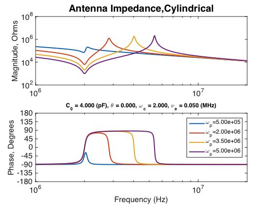
Magnitude and phase plots of the theoretical impedance seen on the probe with different
plasma densities are shown in Figure 2.2.
Using these models as background, measurements from a probe in the plasma can be
used to calculate the plasma density at the time of the measurement. It is noted that in
the phase plot that as the plasma density increases the frequency at which the impedance10
Complex Impedance
1
0.8
0.6
0.4
0.2
Magnitude
0
−0.2
−0.4
−0.6 Voltage Input
Phase Shifted Current
−0.8 Magnitude Shifted Current
Magnitude and Phase Shifted Current
−1
0 0.2 0.4 0.6 0.8 1 1.2 1.4 1.6 1.8 2
Time
Fig. 2.1: Example of the effects of impedance11 Fig. 2.2: Theoretical impedance characteristics for a cylindrical probe
12

moves from inductive to capacitive also increases. There is also a maximum value of the

magnitude found at the same frequency. This frequency is referred to as the upper hybrid

frequency. Finding this upper hybrid frequency will be the primary method of calculating

the plasma density.

2.2.1   I/Q Sampling

    The complex impedance of the probe in the plasma, Z, can be represented in either

polar or rectangular form:

                                       Aejφ = I + jQ

where the relation between I,Q and A, φ is given by:

                                            p
                                       A=    I 2 + Q2                                     (2.1)


                                                −1       Q
                                      φ = tan                                             (2.2)
                                                         I

                                         I = Acos(φ)                                      (2.3)

                                        Q = Asin(φ).                                      (2.4)

    There are both algorithms and instrumentation to detect either the magnitude/phase

or the I/Q representations of the impedance using either analog or digital systems. Both

magnitude/phase and I/Q require some type of reference signal to compare against so as

to determine the timing of the voltage relative to the current, or phase shift.

    The I/Q representation of the impedance is found through the use of multiplication of

the signal with a reference signal using either an analog mixer or with digital multiplication,

depending where in the signal chain the analog to digital converter is placed. The advent of

high sampling speed analog to digital converters (ADCs) allows for the digitization of the

RF (1–30MHz) current signal directly. The analog mixer and its non-ideal characteristics

are avoided and the I/Q detection can be accomplished using digital processing that is ideal,

noise free, and do not drift with temperature. These are the same techniques as commonly
13
referred to as software-defined radio in which a high speed ADC is followed by digital signal
processing algorithms. Because of these advantages the digital I/Q method will be used in
the USU SIP to detect the impedance of the probe.
Figure 2.3 shows the implementation of the mixing operation. A derivation of this
implementation is as follows.
To calculate the I/Q samples, trigonometric identities are exploited. It is known that
1
cos(α)cos(β) = [cos(α + β) + cos(α − β)]. (2.5)
2
By applying a low-pass filter, the double frequency term can be removed and the
remaining signal is
1
cos(α)cos(β) ≈ [cos(α − β)]. (2.6)
2
If the AC current signal returning from the probe, R, is R = Acos(f + φ) and we have
the signals cos(f ) and cos(f + pi/2) available then by using Equations 2.3, 2.4, and 2.5 we
get:
A I
Rcos(f ) =
cos(φ) = (2.7)
2 2
π A π A Q
Rcos f + = [cos φ − ] = sin(φ) = (2.8)
2 2 2 2 2
Thus, by taking the received signal and multiplying it with cos(f ) and cos(f + π2 ),
then filtering, the I/Q data is directly found. This simplicity is what makes using the I/Q
method an attractive option for impedance measurements. To implement this approach,
Fig. 2.3: Block diagram of the mixing operation14
the cos(f ) and cos(f + π2 ) signals will need to be generated along with the output signal.
Note that cos(f + π2 ) = −sin(f ).
By using Equations 2.1 and 2.2, the magnitude/phase can be found if needed as
s
I 2 Q2
+ = A/2 (2.9)
2 2
!
Q
−1 2
tan I
= φ. (2.10)
2
Lingering scale factors can be compensated for in calibration if needed.
2.2.2 System Overview
The full SIP system to find the I/Q samples is shown in Figure 2.4.
Fig. 2.4: High level diagram of how the I/Q data will be generated
The digital portion of the system will be implemented in a FPGA. The FPGA will
house the start and end of the signal chain and contain all but the signal conditioning and
sampling. The process starts with a numerically controlled oscillator (NCO) to generate
the needed sinusoids. An NCO works by filling a Look-Up Table (LUT) with points of a
sinusoid wave. A phase value is used to address the LUT and output the appropriate value
to the Digital-to-Analog converter (DAC) which is later filtered. Along with the cosine
output signal, a negative sine signal is output for calculations later.
The DAC output is sent through a reconstruction filter. The reconstruction filter is15
a low-pass filter (LPF) with a steep cutoff to change the digital stepped sinusoid that is
output by the DAC into a smooth sinusoid. This smoothed signal goes to the RF Head and
the probe in the plasma. The RF Head consists of a set of transformers that decouple the
probe from the loads further down the analog chain that would affect the impedance seen
at the probe.
After passing through the probe, an impeded signal is sampled by a high speed ADC.
After being sampled by the ADC, the now digital signal is mixed with the original cosine
and a negative sine signal. These mixed signals are then low-pass filtered to get the I/Q
samples for further processing such as a tracking control loop.
There will be noise present in the I/Q samples that come from sources such as a
non-ideal original signal, non-ideal Analog-to-Digital conversion, other instruments on the
spacecraft, and so on. Multiple strategies could be employed to improve the inherent noise
on the data. Additional filtering to smooth the I/Q sample stream is one method that
could be used. Oversampling and averaging would also provide improved samples but more
simply. Both oversampling and filtering will be employed for the USU SIP.
This system can meet all of the defined requirements derived from the overall mission
requirements. As the individual components were chosen and digital system designed,
care was taken to generate samples at the prescribed rates while meeting noise and power
requirements.
2.3 SPORT Mission Requirements
The Scintillation Prediction Observation Research Task (SPORT) mission is tasked
with answering two science questions:
1. What is the state of the ionosphere that gives rise to the growth of plasma irregularities
that extend into and above the F-peak?
2. How are plasma irregularities at satellite altitudes related to the radio scintillations
observed passing through these regions?16
In order to answer these questions, mission science requirements have been defined.
These requirements are given in Table 2.1. These requirements were developed according to
the concept of a minimum mission science requirements set, such that if these requirements
are achieved then progress can be made on the science questions. These requirements cover
what all instruments on the space craft need to accomplish together.
Table 2.1: Top level requirements for the SPORT mission
The Scintillation Prediction Observation Research Task Instrumentation Spacecraft
Observational Science Measurement Instrument Space System
Approach Requirements Approach Requirements
1) What is the state of the ionosphere that gives rise to the growth of plasma irregularities that extend into
and above the F-peak?
GPS Occultation
Observations in the
1700 to 0100 LT sector
Plasma Density Profile Observe GPS satellite Satellite Orbit
over -30 to 30 latitude
1) 140 to 450 km alt occultation along 1) 1 year mission life
2) 104 to 107 p/cm3 range and to the sides of the 2) 40 to 55 inclination
Height profiles of the
3) 20% p/cm3 accuracy orbit plane to obtain 3) 350 to 450 km altitude
plasma density to specify
4) 1000 km along track sampling line of site TEC 4) 10 km eccentricity
the magnitude and height
of the F peak density in
Ion Drifts (Earth Reference Frame) Ion Velocity Meter Spacecraft
the EA
1) 800 m/s Range 1) 515 Ram Pointing 1
2) 20,m/s precision & accuracy Observe vertical ion 2) 1 km position knowledge
Vertical ion drifts at or
3) 10 km along track sampling drifts by angle of 3) 10 ms timing
below the F peak in the
arrival of heavy ions
EA
at detector
2) How are plasma irregularities at satellite altitudes related to the radio scintillations observed passing
through these regions?
E-Field Double Probe
Observe probe floating
E-Field (Earth Reference Frame)
potential for AC
1) 45,mV/m range
E-fields from irregularity
2) 1.1 mV/m precision & accuracy
Observations in the 2200 3) 1 km along track sampling
GPS Occultation
to 0200 LT sector over 4) 10 km - 200 m along track waves
S4 scintillation index
-30 to 30 latitude Spacecraft Mechanisms
Plasma Density 1) 0.6 m tip-to-tip booms
Langmuir/Impedance
Observations of 1) 103 to 107 p/cm3 range
Observe DC and AC
irregularities in electron 2) 103 p/cm3 precision & accuracy Attitude
probe response for
density and E-field power 3) 1 km along track sampling (Post Flight Knowledge)
relative and absolute
spectral density in 4) 10 km - 200 m along track waves 1) 0.05 1-uncertainty
electron density
slope from 200 km to
and observe irregularities
200 m B-field
1) 56,000 nT range
Three Axis Magnetometer
2) 100 nT precision and accuracy
Support VxB computation
3) 1 km along track sampling
for ion velocity and
E-Field measurements17
2.4 Plasma Measurement Requirements
The requirements developed for the SPORT mission were used to develop engineering
requirements for the Sweeping Impedance Probe (SIP) on the USU Space Weather Instru-
ment. These requirements are given in Table 2.2.
Table 2.2: Derived Requirements for the USU SIP
ID Description
R1 The Sweeping Impedance Probe (SIP) shall have both Sweeping and Tracking
functionality
R2 The SIP shall make measurements in the driving frequency range of 1MHz to
30MHz
R3 A SIP sweep shall consist of 512 measurement steps made at associated driving
frequencies
R4 The frequency associated with each step in a SIP sweep shall be reconfigurable
during flight
R5 The measurement period for each sweep step shall have a duration of 2.5 ms
R6 A SIP sweep shall be completed within18
a table on the probe. This allows for any type of sweep: linear, triangular, or focused on
specific frequencies.
This sweeping function helps to confirm the value of the upper hybrid frequency. The
sweeping function will be in addition to the tracking function which is the primary method
of measuring the upper hybrid frequency and by extension the plasma density. Because
of this secondary nature of the sweeping function, sweeps will only happen once every two
minutes (R7).
2.6 Track Function
Whole sweeps are not necessary to calculate the plasma density; only the frequency
where the phase of the impedance goes from positive to negative is needed. If this frequency
can be tracked, then the plasma density can be calculated at a higher rate for a better
sampling of changes in plasma density. Because of this, the tracking mode will be the mode
that the SIP operates under most of the time.
Requirements R8-R12 are in direct reference to this tracking mode. The tracking
system will implement a control loop that calculates the current phase response of the probe
at the current frequency, and then adjust the output frequency accordingly. This control
loop will look for and hold at the zero phase point which is the upper hybrid frequency
(R9). The resistance of the impedance affects the steepness of the change from inductive
to capacitive impedances at the upper hybrid frequency (R10), making it necessary for
the control loop to be accurate. In order to meet the science objectives the probe must
be accurate to within 5 degrees of the true plasma impedance phase (R11). It also must
generate data at a rate of 40Hz to create a detailed enough measurement (R8,12).CHAPTER 3
ANALOG SYSTEM DESIGN
3.1 Concept of Operations of the Sweeping Impedance Probe Analog System
Figure 3.1 presents a high-level concept of operations of the Sweeping Impedance Probe.
The objective of the system is to apply a known voltage to a probe in the plasma, and to
measure the current, i, that flows in response to the applied voltage. The current will be
detected with an ammeter circuit. The challenge is that the voltage source operates at RF
frequencies and the ammeter must measure the vector current, meaning magnitude and
phase of the RF signal. Another challenge is to either keep the impedance associated with
the voltage source and the ammeter low or to have the impedance be well known. This is
so that the voltage across the probe in the plasma is known and that the current flowing
in the circuit is not perturbed by the measurement approach. Of the requirements listed in
Chapter 2, requirements R2, R9, R10, and R11 are the most pertinent to the analog design.
The general approach is to digitally generate the voltage source, apply the voltage
source to the probe, measure the current that goes through the probe, and use the measured
current to find the impedance of the probe. A digital source voltage generation is needed
for the digital calculation of the impedance. If the voltage source was generated by analog
means, more analog components would be needed to sample the voltage source along with
the associated current. Because the voltage source is generated digitally a processing chain
is needed to smooth out the digital, stepped signal to limit the bandwidth of the signal. If
the voltage source is properly generated, the signal spectrum will consist of nearly one single
frequency leading to accurate measurements. The full source generation chain consists of
an NCO housed on the FPGA, a high speed DAC, and filtering. The source generation was
partially moved inside the FPGA by necessity for the digital processing.
Once the voltage source is generated and conditioned it is passed to the probe. The20
A
Fig. 3.1: Conceptual diagram of the analog system
probe is isolated between transformers with one of the transformers being a current trans-
former to convert the current to a voltage for measurement. A high speed ADC then
measures this voltage. In the rest of this chapter each of these elements of the impedance
probe analog electronics will be discussed and will be generally described. How they are
meeting the design requirements will also be discussed.
3.2 Source Generation
To generate the input signal for the probe a narrow-bandwidth voltage signal will need
to be created. Secondary frequency content needs to be as small as possible to not affect
detection of the upper hybrid frequency. Noise on the signal should be low for the same
reason. With these goals in mind, the system seen in Figure 3.2 was used. Full schematics
can be found in Appendix A.
In Figure 3.2 the signal flows as follows:
1. A sinusoid is generated by the FPGA using an NCO
2. The digital sinusoid is sent to a high speed digital to analog Converter (HSDAC)
3. The sinusoid is sent through a Low-Pass filter (LPF) to remove high frequencies21
1 1
ℎ
7
= 0.5
_
Fig. 3.2: Diagram of the Signal Generation chain for the SIP
This system when implemented properly will generate a very clean single frequency
output. The system does have adjustability built in to add further control for a consis-
tent output no matter the frequency being generated. Each portion of this design will be
explained in detail here.
3.2.1 NCO Output and High-Speed DAC
As was discussed in Chapter 2 the generation of the output sinusoid starts inside an
FPGA. The NCO module outputs a value over a parallel bus to a HSDAC for conversion.
The HSDAC used for the USU SIP uses a differential current output instead of a voltage
output. By using a differential current output, the HSDAC is able to decrease noise and
provide a wider voltage range than single ended DACs [13]. To convert the current output
to a voltage, the output currents are passed through a resistor, creating a voltage from the
current difference. The value of the resistor used at the output of the HSDAC depends on
the desired voltage. If a higher voltage is needed, a larger resistor can be used, or smaller
if lower voltages are desired.
The voltage source at this point is stepped because of the digital generation. To remove
these steps and the high frequency content that they contain, the signal is next sent into a
filtering stage. Along with the data input from the NCO, the HSDAC has a full scale adjust
(FS ADJ) input. This input is used in conjunction with the filtering and will be discussed
in section 3.2.2.22
3.2.2 Reconstruction Filter
Because the output sinusoid originates from digital synthesis, rather than an analog
origin, the output is stepped. These steps bring with them high frequency content. This
high frequency content needs to be removed, thus a reconstruction filter is needed. This
concept is illustrated in Figure 3.3.
Fig. 3.3: Conceptual diagram of the reconstruction filter
The reconstruction filter was designed under the following requirements:
1. The filter needs to pass frequencies from 1MHz to 30 MHz, to facilitate full sweeping
and tracking functionality
2. Frequencies higher than 30MHz need to be filtered out as much as possible
3. The passband gain should be as flat as possible to not affect the magnitude measure-
ment when comparing impedances at different frequencies
These design requirements stem from requirements R2, R9, and R11 presented in Chapter
2. The filter architecture that was selected to fulfill these requirements was a 7th order
elliptic filter. Elliptic filters have the highest ratio of passband to stop-band gain but that
comes with a trade-off of ripples in both bands [14].
Ripples in the stop-band have a negligible effect on the filter performance as long as
the overall stop-band is a sufficient number of dBs lower than the passband. Ripples in the
passband, on the other hand, will have a major effect on the accuracy of the impedance
measurement. These ripples can be reduced by careful choice of component values in the
filter, reducing this problem to an extent. The magnitude and phase response of the designed
filter is shown in Figures 3.4 and 3.5, respectively.23 Fig. 3.4: Magnitude Response of the 7th order Elliptic Filter Fig. 3.5: Phase Response of the 7th order Elliptic Filter
24

    Ripples in the passband are still present and need to be addressed to meet the design

requirements. The passband magnitude can be flattened by changing the magnitude of the

signal going into the filter. Along with the primary HSDAC that outputs the sinusoid, a

second DAC is used to control the amplitude of the output signal. The FS ADJ pin on the

HSDAC is used to set the maximum current output from the HSDAC. By using the second

DAC, the FS ADJ pin can be controlled manually, controlling the maximum current output

of the HSDAC. During calibration the magnitude of the filter will be measured at different

frequencies, and the voltage of the DAC can be set per output frequency to smooth the

overall output of the signal generation.

    By maintaining the amplitude of the voltage source and filtering out much of the high

frequency content, the primary source of variation of the probe excitation is the frequency of

the input. This aids in meeting the measurement precision requirements since any variation

other than frequency will affect the calculated impedance.

    In previous missions, including the ASSP mission, to account for the phase response

of the analog system a reference signal was generated. This reference was sent through the

same analog components as the measured signal minus the probe itself. This signal then was

used to perform the mixing. Because the only phase difference between the two signals was

that of the probe, the measured phase offset was accurate. Because the SPORT SIP does

all processing digitally, this method would require a second ADC to sample the reference

channel. It was decided to not use the reference channel method to avoid the extra power

draw that a second ADC would use. The high speed ADC used to sample the probe signal

is one of the highest power parts of the entire analog system, so using two of those parts

was not possible within the targeted power budget. The digital method to compensate for

the analog phase shift is discussed in Chapter 4.

    Op-amps are placed before and after the reconstruction filter to decouple the HSDAC

output, filter, and loads from each other while maintaining the desired characteristics of

each stage. The op-amps were chosen to have sufficiently high gain-bandwidth product,

and low enough noise for this application. Lower noise amplifiers could have been used at
25
the expense of higher power consumption.
3.3 Current Measurement
To measure the impedance of the probe in the plasma the following is needed: to apply
the source to the probe with minimal current leaks or other parasitic impedances, and to
measure the current with as little noise added in the conditioning as possible. Both are
discussed below.
3.3.1 RF Head
Once the generated sinusoid has been filtered it is sent to the probe. The RF Head
is the system that applies the voltage source to the probe and protects the current from
parasitics that would affect measurement accuracy. The RF Head is made of transformers
around the probe connection to aid in isolating the probe effects from any loads or parasitic
currents. Figure 3.6 shows a diagram of the probe in the ionospheric plasma and how it
fits within the RF Head. In Figure 3.6 the probe component includes the physical probe
and the plasma between the probe and the spacecraft. The interaction between the probe,
plasma, and spacecraft body was presented in Chapter 2. For this model of the system, the
probe and plasma act as an R-L-C circuit. This R-L-C circuit can be analyzed by comparing
the voltage and current in the system. As discussed in Chapter 2, if the current can be
measured it can be compared to the voltage using the I/Q method to find the response of
the probe. To capture the current through the probe and plasma a current transformer is
Fig. 3.6: Diagram of the RF Head circuit26
used. The current through the probe side of the transformer is converted to a voltage by a
load resistor and is then measured by an ADC after being amplified.
Preventing parasitic currents is important for accurate measurements. To prevent any
effects on the measurement from these currents, the connection to the probe is guarded.
The probe connection is made with shielded wire. The shielding on the wire is grounded
to prevent parasitic currents from reaching the current at the probe. To have shielded wire
in the transformer, the transformer is hand-wound and attached to the circuit board after
fabrication. The guarding aids in meeting requirements R9 and R10.
At the end of this processing chain is a set of op-amps that amplify the voltage out
of the current transformer. This gain should be as high as is necessary to reach the full
scale input of the ADC. If a signal that is input to the ADC is full scale, the signal will
have peak amplitude equal to the maximum voltage that the ADC can measure. All ADCs
have an amount of noise inherent in the measurement. This noise is commonly measured
in counts in the measurement, where counts is the digital number output by the ADC. By
providing a full scale input the number of counts for the signal is much larger than the
ADC’s measurement noise. This reduces the noise power from the ADC and the overall
noise in the measurement.
3.3.2 Sampling
The final step of the analog system is to sample the data coming from the RF Head.
A diagram of the sampling system is shown in Figure 3.7. The sampling is done with
a High Speed ADC (HSADC). To sample with little noise, a differential ADC is used.
Fig. 3.7: Schematic of Sampling System27 Using a differential ADC requires that the signal to be sampled is encoded in the voltage difference between two input lines. To create this differential signal the circuit in Figure 3.7 is used. This circuit is the suggested method from the data sheet of the HSADC used in the design [15]. For data transmission between the ADC and the FPGA, a parallel bus is used to meet sample rate requirements.
CHAPTER 4

                              DIGITAL SYSTEM DESIGN

    To control all the needed functionality of the SIP, the digital system was designed as

shown in Figure 4.1. Figure 4.1 flows generally from left to right for the system control

and right to left for measurement handling and processing. All major subsystems seen in

the design are detailed later in the chapter. The detailed figures retain the same data flow

directions for comparison to Figure 4.1.

                       Fig. 4.1: Top Level Diagram Digital System

    The system starts with the Mode Control block which toggles between Sweep and Track

mode. The output mode control signal is then fed to the major control blocks. Each major

control block, when enabled, manages the whole probe and set how the data measurements

are organized for packet outputs. Once the mode is set, the mode control blocks will manage

what signal is output to the probe. The Mode Control takes inputs from the microprocessor

to determine which of the modes to be in, or to alternate. If alternating between modes,

the Mode Control will time when the switch will happen (R7).

    The Sweep Control subsystem will output a predefined frequency sweep, via the NCO,
29
measuring the probe impedance in a frequency range of 1-30MHz. The magnitude of the
output of the FS ADJ DAC is also controlled at each step of the sweep. This provides a
constant amplitude signal to the probe to such that any magnitude change on the measure-
ments is only from the probe and not from the other analog components. This subsystem
does not require any external inputs while enabled.
The Track Control subsystem tracks the upper-hybrid frequency of the ionospheric
plasma discussed in Chapter 2. To do this the subsystem receives the filtered I and Q
from the probe and calculates the phase of the probe impedance. At the upper hybrid
frequency the phase equals zero, providing a simple point to track. Using a control loop
with the calculated phase as the input, an output frequency is generated to track the desired
frequency. This generated frequency is sent to the NCO for output and is the data that is
packetized for tracking packets.
The data input from the ADC is first mixed to generate the I and Q data that is
then low-pass filtered and accumulated for use. In sweeping mode the I and Q data is sent
directly out as the sweep data, while the track uses the I and Q data to calculate the phase
offset. The data packetizing consists of gathering the needed data for one granule of the
full packet then handing of the data to the on board microprocessor to build the complete
packets.
The HDL for the system was written in VHDL using state machine style behavioral
design for all controllers while the data processing chain was written as RTL design. The
full development project with all the FPGA HDL and microprocessor C code is included in
Appendix A.
4.1 Signal Generation
The output signal generation system is shown in Figure 4.2. This system outputs the
proper frequency of sinusoid and accounts for the analog system response through which
the signal will pass. By accounting for the analog system response, the impedance of the
probe in the plasma can be isolated.You can also read