DPUCZDX8G FOR ZYNQ ULTRASCALE+ MPSOCS - PRODUCT GUIDE - XILINX
←
→
Page content transcription
If your browser does not render page correctly, please read the page content below
DPUCZDX8G for Zynq
UltraScale+ MPSoCs

Product Guide
PG338 (v4.1) January 23, 2023

Xilinx is creating an environment where employees, customers, and
partners feel welcome and included. To that end, we’re removing non-
inclusive language from our products and related collateral. We’ve
launched an internal initiative to remove language that could exclude
people or reinforce historical biases, including terms embedded in our
software and IPs. You may still find examples of non-inclusive language
in our older products as we work to make these changes and align
with evolving industry standards. Follow this link for more
information.
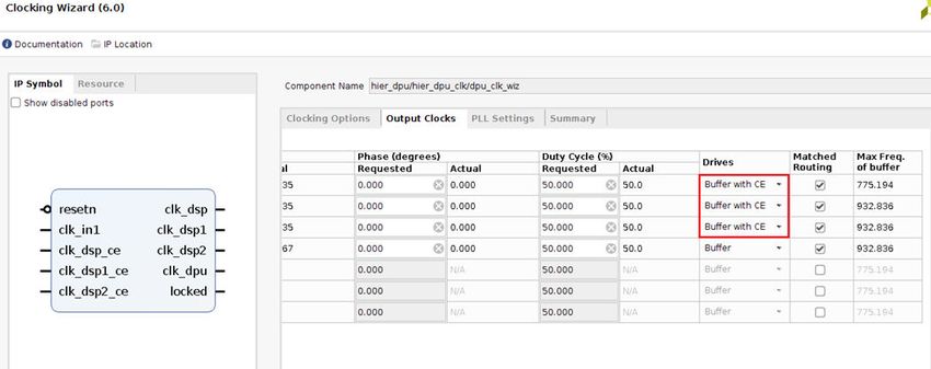
Table of Contents
      Chapter 1: Introduction.............................................................................................. 4
         Features........................................................................................................................................ 4
         IP Facts..........................................................................................................................................5

      Chapter 2: Overview......................................................................................................6
         Core Overview..............................................................................................................................6
         Hardware Architecture............................................................................................................... 7
         Development Tools..................................................................................................................... 9
         MPSoC Integration Example.................................................................................................... 10
         Vitis AI Development Kit........................................................................................................... 11

      Chapter 3: Product Specification......................................................................... 13
         Port Descriptions.......................................................................................................................13
         Register Space........................................................................................................................... 14
         Interrupts................................................................................................................................... 19

      Chapter 4: DPU Configuration............................................................................... 21
         Introduction............................................................................................................................... 21
         Configuration Options.............................................................................................................. 24
         Advanced Tab.............................................................................................................................31
         Summary Tab............................................................................................................................. 32
         DPUCZDX8G Peak Performance ............................................................................................. 33
         Xilinx Model Zoo Performance................................................................................................ 33
         I/O Bandwidth Requirements..................................................................................................36
         Clocking...................................................................................................................................... 36
         Reset........................................................................................................................................... 42

      Chapter 5: Development Flow............................................................................... 44
         Customizing and Generating the Core in the Zynq UltraScale+ MPSoC............................ 44
         Customizing and Generating the Core in the Vitis IDE.........................................................50

      Chapter 6: Example Design..................................................................................... 55

PG338 (v4.1) January 23, 2023                                                                                                       www.xilinx.com
                                                                                                     Send Feedback
DPUCZDX8G for ZynqUltraScale+ MPSoCs                                                                                                             2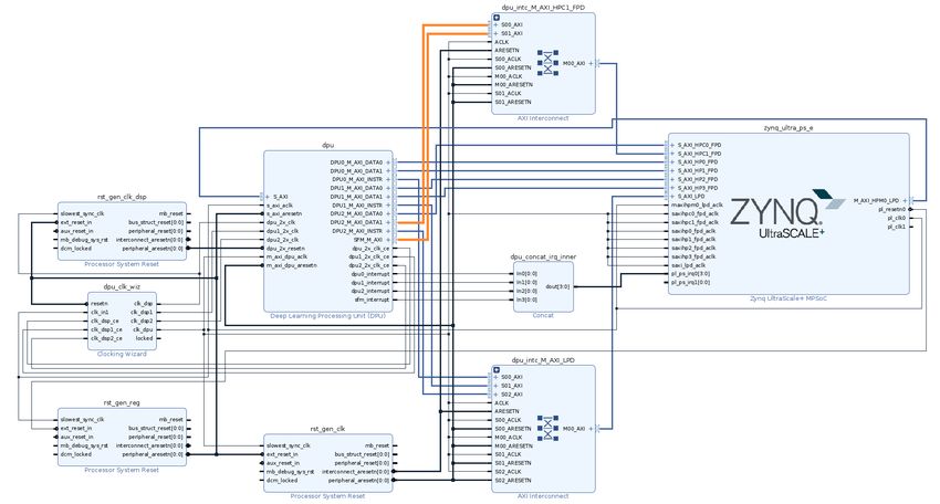
Introduction............................................................................................................................... 55
         Vivado DPU TRD Flow............................................................................................................... 55
         Vitis DPU TRD Flow.................................................................................................................... 56

      Appendix A: Additional Resources and Legal Notices............................. 57
         Xilinx Resources.........................................................................................................................57
         Documentation Navigator and Design Hubs.........................................................................57
         References..................................................................................................................................57
         Revision History......................................................................................................................... 58
         Please Read: Important Legal Notices................................................................................... 61

PG338 (v4.1) January 23, 2023                                                                                                  www.xilinx.com
                                                                                                  Send Feedback
DPUCZDX8G for ZynqUltraScale+ MPSoCs                                                                                                        3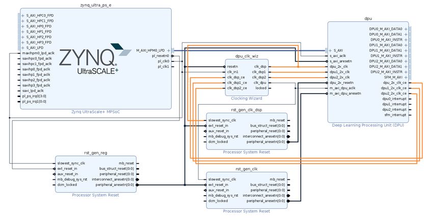
Chapter 1: Introduction

                                                                                     Chapter 1

Introduction
      The DPUCZDX8G is the Deep learning Processor Unit (DPU) designed for the Zynq®
      UltraScale+™ MPSoC. It is a configurable computation engine optimized for convolutional neural
      networks. The degree of parallelism utilized in the engine is a design parameter and can be
      selected according to the target device and application. At a high-level, the DPU is a microcoded
      compute engine which has an efficient, optimized instruction set, and which can support
      inference of most convolutional neural networks.

Features
      • Supports one AXI slave interface for accessing configuration and status registers.
      • Supports one AXI master interface for instruction fetch.
      • Supports individual configuration of each channel.
      • IP is available in multiple variants, scaling both in terms of logic resource utilization and
        parallelism. Configurations include: B512, B800, B1024, B1152, B1600, B2304, B3136, and
        B4096, where the nomenclature indicates the total number of MACs per DPU clock cycle.
      • Software and IP core support for up to a maximum of four homogeneous DPU instances in a
        single AMD Xilinx® SoC.

      The following list highlights key supported operators for the DPUCZDX8G :

      • Supports both Convolution and transposed convolution
      • Depthwise convolution and depthwise transposed convolution
      • Max pooling
      • Average pooling
      • ReLU, ReLU6, Leaky ReLU, Hard Sigmoid, and Hard Swish
      • Elementwise-sum and Elementwise-multiply
      • Dilation
      • Reorg
      • Correlation 1D and 2D
      • Argmax and Max along channel dimension

PG338 (v4.1) January 23, 2023                                                           www.xilinx.com
                                                                     Send Feedback
DPUCZDX8G for ZynqUltraScale+ MPSoCs                                                                 4
Chapter 1: Introduction
• Fully connected layer
• Softmax
• Concat, Batch Normalization
IP Facts
DPUCZDX8G IP Facts Table
Core Specifics
Supported Device Family Zynq® UltraScale+™ MPSoC Family
Supported User Interfaces Memory-mapped AXI interfaces
Resources See Chapter 4: DPU Configuration.
Provided with Core
Design Files Encrypted RTL
Example Design Verilog
Constraints File Xilinx Design Constraints (XDC)
Supported S/W Driver Included in PetaLinux
Test Bench Not Provided
Simulation Model Not Provided
Tested Design Flows
Design Entry Vivado® Design Suite and Vitis™ unified software platform
Simulation N/A
Synthesis Vivado® Synthesis
Xilinx Support web page
Notes:
1. Linux OS and driver support information are available from DPUCZDX8G TRD or Vitis™ AI development kit.
2. For the supported tool versions, see the Vivado Design Suite User Guide: Release Notes, Installation, and Licensing
(UG973).
3. The DPUCZDX8G is driven by instructions generated by the Vitis AI compiler. When the target neural network (NN),
DPUCZDX8G hardware architecture, or AXI data width is changed, the related .xmodel file which contains DPUCZDX8G
instructions must be regenerated with the updated arch.json file.
4. The DPU does not support hw_emu function. The reasons are as follows:
• The RTL code of DPU is encrypted. Vitis™ does not analyze the source code.
• The DPU is a co-processor and would require a highly complex test environment for adequate design verification.
PG338 (v4.1) January 23, 2023 www.xilinx.com
Send Feedback
DPUCZDX8G for ZynqUltraScale+ MPSoCs 5Chapter 2: Overview
Chapter 2
Overview
Core Overview
The Xilinx® DPUCZDX8G is a programmable engine optimized for convolutional neural
networks. It is composed of a high performance scheduler module, a hybrid computing array
module, an instruction fetch unit module, and a global memory pool module. The DPUCZDX8G is
a microcoded engine which uses a specialized instruction set, which allows for the efficient
implementation of many convolutional neural networks. Some examples of convolutional neural
networks which have been deployed include VGG, ResNet, GoogLeNet, YOLO, SSD, MobileNet,
and FPN among others.
The DPUCZDX8G IP is implemented in the programmable logic (PL) of the selected Zynq®
UltraScale+™ MPSoC device with direct connections to the processing system (PS). The
DPUCZDX8G executes compiled microcode generated from a neural network graph, and
requires accessible memory locations for input images as well as temporary and output data. A
program running on the application processing unit (APU) is also required to service interrupts
and coordinate data transfers.
The top-level block diagram of the DPUCZDX8G is shown in the following figure.
PG338 (v4.1) January 23, 2023 www.xilinx.com
Send Feedback
DPUCZDX8G for ZynqUltraScale+ MPSoCs 6Chapter 2: Overview
Figure 1: DPUCZDX8G Top-Level Block Diagram
High
PE PE PE PE
Performance
Scheduler
Hybrid Computing Array
APU
Instruction
Global Memory Pool
Fetch Unit
DPU
High Speed Data Pipe
External DDR RAM
X22327-072219
where,
• APU - Application Processing Unit
• PE - Processing Engine
• DPU - Deep Learning Processing Unit
Hardware Architecture
The detailed hardware architecture of the DPUCZDX8G is shown in the following figure. After
start-up, the DPUCZDX8G fetches instructions from off-chip memory to control the operation of
the computing engine. The instructions are generated by the Vitis™ AI compiler, which performs
substantial optimizations including layer fusion.
PG338 (v4.1) January 23, 2023 www.xilinx.com
Send Feedback
DPUCZDX8G for ZynqUltraScale+ MPSoCs 7Chapter 2: Overview
On-chip memory is used to buffer input activations, intermediate feature-maps, and output
meta-data to achieve high throughput and efficiency. The data is reused as much as possible to
reduce external memory bandwidth requirements. A deep pipelined design is used for the
computing engine. The processing elements (PEs) take full advantage of the fine-grained building
blocks such as multipliers, adders, and accumulators in Xilinx devices.
Figure 2: DPUCZDX8G Hardware Architecture
Off-Chip Memory
Processing System (PS)
CPU Memory Controller
Bus
On-Chip Buffer
Fetcher Data Mover
Instruction
Scheduler
Controller
Decoder On-Chip BRAM
Dispatcher BRAM Reader/Writer
Computing
Engines
Engine
Engine
Conv
PE PE PE Misc
Programmable Logic (PL)
X22332-022420
DPUCZDX8G with Enhanced Usage of DSP
A DSP Double Data Rate (DDR) technique may be used to used to improve the performance
achieved with the DPU. In this configuration, two input clocks for the DPUCZDX8G are needed:
A 1x clock for general logic and a 2x clock for DSP slices are employed. For more information,
see Clocking. The difference between a DPUCZDX8G not using the DSP DDR technique and a
DPUCZDX8G enhanced usage architecture is shown in the following image.
Note: All DPUCZDX8G architectures referred to in this document refer to DPUCZDX8G enhanced usage,
unless otherwise specified.
PG338 (v4.1) January 23, 2023 www.xilinx.com
Send Feedback
DPUCZDX8G for ZynqUltraScale+ MPSoCs 8Chapter 2: Overview
Figure 3: DPUCZDX8G with (Enhanced Usage) and without DSP DDR
clk1x clk2x clk1x
clk1x PCOUT
IMG A IMG A A A
ram ram Async DLY
RES RES OUT
+ A+D + A+D 0 0 0
DLY
IMG D IMG D D D
ram × M RES ram DLY ×
Async M
P
PCOUT
+
RES OUT
WGT B B WGT B0 B B B
1 1
ram ram Async SEL
DSP48 Slice DSP48 Slice
WGT B1
ram Async
PCIN
Without DSP DDR
Enhanced Usage
X22333-111120
Development Tools
Two flows are supported for integrating the DPUCZDX8G into your project: the Vivado flow and
the Vitis™ flow.
The Xilinx Vivado® Design Suite is required to integrate the DPUCZDX8G into your projects for
the Vivado flow. Vivado Design Suite 2022.2 or later version is recommended. Contact your local
sales representative if the project requires an older version of Vivado.
The Vitis unified software platform 2022.2 or later is required to integrate the DPUCZDX8G for
the Vitis flow.
DPUCZDX8G Development Flow
The DPUCZDX8G requires a device driver which is included in the Xilinx Vitis™ AI development
kit.
Free developer resources can be obtained from the Xilinx website: https://github.com/Xilinx/
Vitis-AI.
The Vitis AI User Guide (UG1414) describes how to use the DPUCZDX8G with the Vitis AI tools.
The basic development flow is shown in the following figure. First, use Vivado or Vitis to
generate the bitstream. Then, download the bitstream to the target board and install the related
driver. For instructions on installing the related driver and dependent libraries, see the Vitis AI
User Guide (UG1414).
PG338 (v4.1) January 23, 2023 www.xilinx.com
Send Feedback
DPUCZDX8G for ZynqUltraScale+ MPSoCs 9Chapter 2: Overview
Figure 4: HW/SW Stack
Example NN Inference Third Party NN Inference
Application Application
Vitis AI APIs
Vitis AI Runtime
DPU IP XRT
PDI
Vitis Hardware Platform
X22328-031620
MPSoC Integration Example
The following image illustrates an example system in which the video frames are captured by a
Zynq® UltraScale+™ MPSoC device with a connected MIPI camera. The DPUCZDX8G is
integrated into the system through an AXI interconnect to perform deep learning inference tasks
such as image classification, object detection, and semantic segmentation.
PG338 (v4.1) January 23, 2023 www.xilinx.com
Send Feedback
DPUCZDX8G for ZynqUltraScale+ MPSoCs 10Chapter 2: Overview
Figure 5: Example System with Integrated DPUCZDX8G
Processing
Arm System (PS)
DisplayPort Arm Cortex-
USB3.0 Cortex
A53
SATA3.1 -R5
PCIe Gen2
GigE
USB2.0
UART Controller DDR
SPI AXI Interconnect
Quad SPI
NAND
SD
AXI Interconnect
AXI AXI
DMA
Interconnect Interconnect
Color_
demosaic gamma
conversion
MIPI MIPI DPU
Camera
CSI2
Programmable
CSI2
Logic (PL)
X22329-081919
Vitis AI Development Kit
The Vitis™ AI development environment is used for AI inference on Xilinx® hardware platforms.
It consists of optimized IP cores, tools, libraries, models, and example designs.
As shown in the following figure, the Vitis AI development kit consists of the AI Compiler, AI
Quantizer, AI Optimizer, AI Profiler, AI Library, and Xilinx Runtime Library (XRT).
PG338 (v4.1) January 23, 2023 www.xilinx.com
Send Feedback
DPUCZDX8G for ZynqUltraScale+ MPSoCs 11Chapter 2: Overview
Figure 6: Vitis AI Stack
User Application
Model Formats
Vitis AI Models Model Zoo Custom Models
AI Compiler | AI Quantizer | AI Optimizer
Vitis AI
Development Kit
AI Profiler | AI Library
Vitis AI Runtime (VART)
Overlay Deep Learning Processing Unit (DPU)
X27682-011823
Further details of the Vitis AI development kit can be found in the Vitis AI User Guide (UG1414).
Note: The Vitis AI development kit is a free download, available from here.
PG338 (v4.1) January 23, 2023 www.xilinx.com
Send Feedback
DPUCZDX8G for ZynqUltraScale+ MPSoCs 12Chapter 3: Product Specification
Chapter 3
Product Specification
Port Descriptions
The DPUCZDX8G top-level interfaces are shown in the following figure.
Figure 7: Two DPU Kernel Ports
The DPUCZDX8G I/O signals are listed and described in the table below.
Table 1: DPUCZDX8G Signal Description
Signal Name Interface Type Width I/O Description
S_AXI Memory mapped AXI 32 I/O 32-bit memory mapped AXI interface
slave interface for registers.
s_axi_aclk Clock 1 I AXI clock input for S_AXI
s_axi_aresetn Reset 1 I Active-Low reset for S_AXI
dpu_2x_clk Clock 1 I Input clock used for DSP blocks in
the DPUCZDX8G. The frequency is
twice that of m_axi_dpu_aclk.
dpu_2x_resetn Reset 1 I Active-Low reset for DSP blocks
PG338 (v4.1) January 23, 2023 www.xilinx.com
Send Feedback
DPUCZDX8G for ZynqUltraScale+ MPSoCs 13Chapter 3: Product Specification
Table 1: DPUCZDX8G Signal Description (cont'd)
Signal Name Interface Type Width I/O Description
m_axi_dpu_aclk Clock 1 I Input clock used for DPUCZDX8G
general logic.
m_axi_dpu_aresetn Reset 1 I Active-Low reset for DPUCZDX8G
general logic
DPUx_M_AXI_INSTR Memory mapped AXI 32 I/O 32-bit memory mapped AXI interface
master interface for DPUCZDX8G instruction fetch.
DPUx_M_AXI_DATA0 Memory mapped AXI 128 I/O 128-bit for Zynq UltraScale+ MPSoC
master interface series.
DPUx_M_AXI_DATA1 Memory mapped AXI 128 I/O 128-bit for Zynq UltraScale+ MPSoC
master interface series.
dpux_interrupt Interrupt 1 O Active-High interrupt output from
DPUCZDX8G.
SFM_M_AXI (optional) Memory mapped AXI 128 I/O Memory-mapped AXI interface for
master interface softmax data.
sfm_interrupt (optional) Interrupt 1 O Active-High interrupt output from
softmax module.
dpu_2x_clk_ce (optional) Clock enable 1 O Active-High clock-enable which is
used to gate the 2x_clk input when
clock gating is enabled.
Notes:
1. The softmax interface is present only when the softmax option for the DPUCZDX8G is enabled.
Register Space
The DPUCZDX8G IP implements registers in programmable logic. The following tables show the
DPUCZDX8G IP registers. These registers are accessible from the APU through the S_AXI
interface.
reg_dpu_reset
The reg_dpu_reset register controls the resets of all DPUCZDX8G cores integrated in the
DPUCZDX8G IP. The lower four bits of this register control the reset of up to four DPUCZDX8G
cores. All the reset signals are active-High. The details of reg_dpu_reset are shown in the
following table.
Table 2: reg_dpu_reset
Address
Register Width Type Description
Offset
reg_dpu_reset 0x004 32 R/W [n] – DPUCZDX8G core n reset
PG338 (v4.1) January 23, 2023 www.xilinx.com
Send Feedback
DPUCZDX8G for ZynqUltraScale+ MPSoCs 14Chapter 3: Product Specification
reg_dpu_isr
The reg_dpu_isr register represents the interrupt status of all cores in the DPUCZDX8G IP. The
lower four bits of this register shows the interrupt status of up to four DPUCZDX8G cores. The
details of reg_dpu_irq are shown in the following table.
Table 3: reg_dpu_isr
Address
Register Width Type Description
Offset
reg_dpu_isr 0x608 32 R [n] – DPUCZDX8G core n interrupt status
reg_dpu_start
The reg_dpu_start register is the start signal for a DPUCZDX8G core. There is one start register
for each DPUCZDX8G core. The details of reg_dpu_start are shown in the following table.
Table 4: reg_dpu_start
Address
Register Width Type Description
Offset
reg_dpu0_start 0x220 32 R/W DPUCZDX8G core0 start signal.
reg_dpu1_start 0x320 32 R/W DPUCZDX8G core1 start signal.
reg_dpu2_start 0x420 32 R/W DPUCZDX8G core2 start signal.
reg_dpu3_start 0x520 32 R/W DPUCZDX8G core3 start signal.
reg_dpu_instr_addr
The reg_dpu_instr_addr register is used to indicate the instruction address of a DPUCZDX8G
core. Each DPUCZDX8G core has a reg_dpu_instr_addr register. Only the lower 28-bits are valid.
In the DPUCZDX8G processor, the real instruction-fetch address is a 40-bit signal which consists
of the lower 28 bits of reg_dpu_instr_addr followed by 12 zero bits. The available instruction
address for DPU ranges from 0x1000 to 0xFFFF_FFFF_FFFF_F000. The details of
reg_dpu_instr_addr are shown in the following table.
Table 5: reg_dpu_instr_addr
Address
Register Width Type Description
Offset
reg_dpu0_instr_addr 0x20C 32 R/W Start address in external memory for
DPUCZDX8G core0 instructions. The lower
28-bit is valid.
reg_dpu1_instr_addr 0x30C 32 R/W Start address in external memory for
DPUCZDX8G core1 instructions. The lower
28-bit is valid.
PG338 (v4.1) January 23, 2023 www.xilinx.com
Send Feedback
DPUCZDX8G for ZynqUltraScale+ MPSoCs 15Chapter 3: Product Specification
Table 5: reg_dpu_instr_addr (cont'd)
Address
Register Width Type Description
Offset
reg_dpu2_instr_addr 0x40C 32 R/W Start address in external memory for
DPUCZDX8G core2 instructions. The lower
28-bit is valid.
reg_dpu3_instr_addr 0x50C 32 R/W Start address in external memory for
DPUCZDX8G core3 instructions. The lower
28-bit is valid.
reg_dpu_base_addr
The reg_dpu_base_addr register is used to indicate the address of input image and parameters for
each DPUCZDX8G in external memory. The width of a DPUCZDX8G base address is 40 bits so it
can support an address space up to 1 TB. All registers are 32 bits wide, so two registers are
required to represent a 40-bit wide base address. reg_dpu0_base_addr0_l represents the lower
32 bits of base_address0 in DPUCZDX8G core0 and reg_dpu0_base_addr0_h represents the
upper eight bits of base_address0 in DPUCZDX8G core0.
There are eight groups of DPUCZDX8G base addresses for each DPUCZDX8G core and thus 32
groups of DPUCZDX8G base addresses for up to four DPUCZDX8G cores. The details of
reg_dpu_base_addr are shown in the following table.
Table 6: reg_dpu_base_addr
Address
Register Width Type Description
Offset
reg_dpu0_base_addr0_l 0x224 32 R/W The lower 32 bits of base_address0 of
DPUCZDX8G core0.
reg_dpu0_base_addr0_h 0x228 32 R/W The lower 8 bits in the register represent
the upper 8 bits of base_address0 of
DPUCZDX8G core0.
reg_dpu0_base_addr1_l 0x22C 32 R/W The lower 32 bits of base_address1 of
DPUCZDX8G core0.
reg_dpu0_base_addr1_h 0x230 32 R/W The lower 8 bits in the register represent
the upper 8 bits of base_address1 of
DPUCZDX8G core0.
reg_dpu0_base_addr2_l 0x234 32 R/W The lower 32 bits of base_address2 of
DPUCZDX8G core0.
reg_dpu0_base_addr2_h 0x238 32 R/W The lower 8 bits in the register represent
the upper 8 bits of base_address2 of
DPUCZDX8G core0.
reg_dpu0_base_addr3_l 0x23C 32 R/W The lower 32 bits of base_address3 of
DPUCZDX8G core0.
reg_dpu0_base_addr3_h 0x240 32 R/W The lower 8 bits in the register represent
the upper 8 bits of base_address3 of
DPUCZDX8G core0.
reg_dpu0_base_addr4_l 0x244 32 R/W The lower 32 bits of base_address4 of
DPUCZDX8G core0.
PG338 (v4.1) January 23, 2023 www.xilinx.com
Send Feedback
DPUCZDX8G for ZynqUltraScale+ MPSoCs 16Chapter 3: Product Specification
Table 6: reg_dpu_base_addr (cont'd)
Address
Register Width Type Description
Offset
reg_dpu0_base_addr4_h 0x248 32 R/W The lower 8 bits in the register represent
the upper 8 bits of base_address4 of
DPUCZDX8G core0.
reg_dpu0_base_addr5_l 0x24C 32 R/W The lower 32 bits of base_address5 of
DPUCZDX8G core0.
reg_dpu0_base_addr5_h 0x250 32 R/W The lower 8 bits in the register represent
the upper 8 bits of base_address5 of
DPUCZDX8G core0.
reg_dpu0_base_addr6_l 0x254 32 R/W The lower 32 bits of base_address6 of
DPUCZDX8G core0.
reg_dpu0_base_addr6_h 0x258 32 R/W The lower 8 bits in the register represent
the upper 8 bits of base_address6 of
DPUCZDX8G core0.
reg_dpu0_base_addr7_l 0x25C 32 R/W The lower 32 bits of base_address7 of
DPUCZDX8G core0.
reg_dpu0_base_addr7_h 0x260 32 R/W The lower 8 bits in the register represent
the upper 8 bits of base_address7 of
DPUCZDX8G core0.
reg_dpu1_base_addr0_l 0x324 32 R/W The lower 32 bits of base_address0 of
DPUCZDX8G core1.
reg_dpu1_base_addr0_h 0x328 32 R/W The lower 8 bits in the register represent
the upper 8 bits of base_address0 of
DPUCZDX8G core1.
reg_dpu1_base_addr1_l 0x32C 32 R/W The lower 32 bits of base_address1 of
DPUCZDX8G core1.
reg_dpu1_base_addr1_h 0x330 32 R/W The lower 8 bits in the register represent
the upper 8 bits of base_address1 of
DPUCZDX8G core1.
reg_dpu1_base_addr2_l 0x334 32 R/W The lower 32 bits of base_address2 of
DPUCZDX8G core1.
reg_dpu1_base_addr2_h 0x338 32 R/W The lower 8 bits in the register represent
the upper 8 bits of base_address2 of
DPUCZDX8G core1.
reg_dpu1_base_addr3_l 0x33C 32 R/W The lower 32 bits of base_address3 of
DPUCZDX8G core1.
reg_dpu1_base_addr3_h 0x340 32 R/W The lower 8 bits in the register represent
the upper 8 bits of base_address3 of
DPUCZDX8G core1.
reg_dpu1_base_addr4_l 0x344 32 R/W The lower 32 bits of base_address4 of
DPUCZDX8G core1.
reg_dpu1_base_addr4_h 0x348 32 R/W The lower 8 bits in the register represent
the upper 8 bits of base_address4 of
DPUCZDX8G core1.
reg_dpu1_base_addr5_l 0x34C 32 R/W The lower 32 bits of base_address5 of
DPUCZDX8G core1.
reg_dpu1_base_addr5_h 0x350 32 R/W The lower 8 bits in the register represent
the upper 8 bits of base_address5 of
DPUCZDX8G core1.
reg_dpu1_base_addr6_l 0x354 32 R/W The lower 32 bits of base_address6 of
DPUCZDX8G core1.
PG338 (v4.1) January 23, 2023 www.xilinx.com
Send Feedback
DPUCZDX8G for ZynqUltraScale+ MPSoCs 17Chapter 3: Product Specification
Table 6: reg_dpu_base_addr (cont'd)
Address
Register Width Type Description
Offset
reg_dpu1_base_addr6_h 0x358 32 R/W The lower 8 bits in the register represent
the upper 8 bits of base_address6 of
DPUCZDX8G core1.
reg_dpu1_base_addr7_l 0x35C 32 R/W The lower 32 bits of base_address7 of
DPUCZDX8G core1.
reg_dpu1_base_addr7_h 0x360 32 R/W The lower 8 bits in the register represent
the upper 8 bits of base_address7 of
DPUCZDX8G core1.
reg_dpu2_base_addr1_l 0x42C 32 R/W The lower 32 bits of base_address1 of
DPUCZDX8G core2.
reg_dpu2_base_addr1_h 0x430 32 R/W The lower 8 bits in the register represent
the upper 8 bits of base_address1 of
DPUCZDX8G core2.
reg_dpu2_base_addr2_l 0x434 32 R/W The lower 32 bits of base_address2 of
DPUCZDX8G core2.
reg_dpu2_base_addr2_h 0x438 32 R/W The lower 8 bits in the register represent
the upper 8 bits of base_address2 of
DPUCZDX8G core2.
reg_dpu2_base_addr3_l 0x43C 32 R/W The lower 32 bits of base_address3 of
DPUCZDX8G core2.
reg_dpu2_base_addr3_h 0x440 32 R/W The lower 8 bits in the register represent
the upper 8 bits of base_address3 of
DPUCZDX8G core2.
reg_dpu2_base_addr4_l 0x444 32 R/W The lower 32 bits of base_address4 of
DPUCZDX8G core2.
reg_dpu2_base_addr4_h 0x448 32 R/W The lower 8 bits in the register represent
the upper 8 bits of base_address4 of
DPUCZDX8G core2.
reg_dpu2_base_addr5_l 0x44C 32 R/W The lower 32 bits of base_address5 of
DPUCZDX8G core2.
reg_dpu2_base_addr5_h 0x450 32 R/W The lower 8 bits in the register represent
the upper 8 bits of base_address5 of
DPUCZDX8G core2.
reg_dpu2_base_addr6_l 0x454 32 R/W The lower 32 bits of base_address6 of
DPUCZDX8G core2.
reg_dpu2_base_addr6_h 0x458 32 R/W The lower 8 bits in the register represent
the upper 8 bits of base_address6 of
DPUCZDX8G core2.
reg_dpu2_base_addr7_l 0x45C 32 R/W The lower 32 bits of base_address7 of
DPUCZDX8G core2.
reg_dpu2_base_addr7_h 0x460 32 R/W The lower 8 bits in the register represent
the upper 8 bits of base_address7 of
DPUCZDX8G core2.
reg_dpu3_base_addr0_l 0x524 32 R/W The lower 32 bits of base_address0 of
DPUCZDX8G core3.
reg_dpu3_base_addr0_h 0x528 32 R/W The lower 8 bits in the register represent
the upper 8 bits of base_address0 of
DPUCZDX8G core3.
reg_dpu3_base_addr1_l 0x52C 32 R/W The lower 32 bits of base_address1 of
DPUCZDX8G core3.
PG338 (v4.1) January 23, 2023 www.xilinx.com
Send Feedback
DPUCZDX8G for ZynqUltraScale+ MPSoCs 18Chapter 3: Product Specification
Table 6: reg_dpu_base_addr (cont'd)
Address
Register Width Type Description
Offset
reg_dpu3_base_addr1_h 0x530 32 R/W The lower 8 bits in the register represent
the upper 8 bits of base_address1 of
DPUCZDX8G core3.
reg_dpu3_base_addr2_l 0x534 32 R/W The lower 32 bits of base_address2 of
DPUCZDX8G core3.
reg_dpu3_base_addr2_h 0x538 32 R/W The lower 8 bits in the register represent
the upper 8 bits of base_address2 of
DPUCZDX8G core3.
reg_dpu3_base_addr3_l 0x53C 32 R/W The lower 32 bits of base_address3 of
DPUCZDX8G core3.
reg_dpu3_base_addr3_h 0x540 32 R/W The lower 8 bits in the register represent
the upper 8 bits of base_address3 of
DPUCZDX8G core3.
reg_dpu3_base_addr4_l 0x544 32 R/W The lower 32 bits of base_address4 of
DPUCZDX8G core3.
reg_dpu3_base_addr4_h 0x548 32 R/W The lower 8 bits in the register represent
the upper 8 bits of base_address4 of
DPUCZDX8G core3.
reg_dpu3_base_addr5_l 0x54C 32 R/W The lower 32 bits of base_address5 of
DPUCZDX8G core3.
reg_dpu3_base_addr5_h 0x550 32 R/W The lower 8 bits in the register represent
the upper 8 bits of base_address5 of
DPUCZDX8G core3.
reg_dpu3_base_addr6_l 0x554 32 R/W The lower 32 bits of base_address6 of
DPUCZDX8G core3
reg_dpu3_base_addr6_h 0x558 32 R/W The lower 8 bits in the register represent
the upper 8 bits of base_address6 of
DPUCZDX8G core3.
reg_dpu3_base_addr7_l 0x55C 32 R/W The lower 32 bits of base_address7 of
DPUCZDX8G core3.
reg_dpu3_base_addr7_h 0x560 32 R/W The lower 8 bits in the register represent
the upper 8 bits of base_address7 of
DPUCZDX8G core3.
Interrupts
A high state on reg_dpu0_start signals the start of a DPUCZDX8G task for DPUCZDX8G core0.
At the end of the task, the DPUCZDX8G generates an interrupt to signal the completion of a
task, and bit0 in reg_dpu_isr is set to 1. The position of the active bit in the reg_dpu_isr depends
on the number of DPUCZDX8G cores. For example, when DPUCZDX8G core1 finishes a task
while DPUCZDX8G core0 is still processing, reg_dpu_isr would contain 2’b10.
PG338 (v4.1) January 23, 2023 www.xilinx.com
Send Feedback
DPUCZDX8G for ZynqUltraScale+ MPSoCs 19Chapter 3: Product Specification
The DPU IP may be configured to instantiate 1-4 cores (see Chapter 4: DPU Configuration). The
IP wrapper for the configured DPU will have up to four dpux_interrupt signals,
corresponding to the number of cores. These signals must be routed through a concat block, and
then be connected to the PS as illustrated in the following image.
Figure 8: Interrupt Concatenation for Multiple DPU Cores
Note:
1. irq7~irq0 corresponds to pl_ps_irq0[7:0].
2. irq15~irq8 corresponds to pl_ps_irq1[7:0].
PG338 (v4.1) January 23, 2023 www.xilinx.com
Send Feedback
DPUCZDX8G for ZynqUltraScale+ MPSoCs 20Chapter 4: DPU Configuration
Chapter 4
DPU Configuration
Introduction
The DPUCZDX8G IP provides some user-configurable parameters to optimize resource usage
and customize different features. Different configurations can be selected for DSP slices, LUT,
block RAM, and UltraRAM usage based on the amount of available programmable logic
resources. There are also options for additional functions, such as channel augmentation, average
pooling, depthwise convolution, and softmax. Furthermore, there is an option to determine the
number of DPUCZDX8G cores that will be instantiated in a single DPUCZDX8G IP.
The deep neural network features and the associated parameters supported by the DPUCZDX8G
are shown in the following table.
A configuration file named arch.json is generated during the Vivado or Vitis flow. The
arch.json file is used by the Vitis AI Compiler for model compilation. If the content of
arch.json is changed. Please re-compile the model. For more information of Vitis AI Compiler,
see refer to the Vitis AI User Guide (UG1414).
In the Vivado flow, the arch.json file is located at $TRD_HOME/prj/Vivado/
srcs/top/ip/top_dpu_0/arch.json.
In the Vitis flow, the arch.json file is located at $TRD_HOME/prj/Vitis/
binary_container_1/link/vivado/vpl/prj/prj.gen/sources_1/bd/
zcu102_base/ip/zcu102_base_DPUCZDX8G_1_0/arch.json.
Note: $TRD_home = Vitis-AI/dsa/DPU-TRD/
PG338 (v4.1) January 23, 2023 www.xilinx.com
Send Feedback
DPUCZDX8G for ZynqUltraScale+ MPSoCs 21Chapter 4: DPU Configuration
Table 7: DPUCZDX8G Operation and Parameter Support
Features Description
Convolution Kernel Sizes w, h: [1, 16]
Strides w, h: [1, 8]
Padding w: [0, kernel_w-1]
h: [0, kernel_h-1]
Input Size Arbitrary
Input Channel kernel_w * kernel_h * ceil(input_channel / channel_parallel)Chapter 4: DPU Configuration
Table 7: DPUCZDX8G Operation and Parameter Support (cont'd)
Features Description
Max Pooling Kernel Sizes w, h: [1, 256]
Strides w, h: [1, 256]
Padding w: [0, min(kernel_w-1,15)]
h: [0, min(kernel_h-1,15)]
Average Pooling Kernel Sizes w, h: [1, 256]
Strides w, h: [1, 256]
Padding w: [0, min(kernel_w-1,15)]
h: [0, min(kernel_h-1,15)]
Elementwise-Sum Input channel 1~256 * channel_parallel
Input size Arbitrary
Feature Map Number 1~4
Elementwise-Multiply Input channel 1~256 * channel_parallel
Input size Arbitrary
Feature Map Number 2
Concat Output channel 1~256 * channel_parallel
Reorg Strides stride * stride * input_channel ≤ 256 * channel_parallel
Fully Connected Input_channel Input_channel ≤ 2048 * channel_parallel
Output_channel Arbitrary
Notes:
1. The parameter channel_parallel is determined by the DPUCZDX8G configuration. For example, channel_parallel for
the B1152 is 12, and channel_parallel for B4096 is 16 (see Parallelism for Different Convolution Architectures table in
Configuration Options section).
2. In some neural networks, the FC layer is connected with a Flatten layer. The Vitis AI compiler will automatically
combine Flatten+FC to a global CONV2D layer, and the CONV2D kernel size is equal to the input feature map size of
Flatten layer. For this case, the input feature map size cannot exceed this automatically configured CONV2D kernel
size, otherwise an error will be generated during compilation. If there is no flatten layer, the FC layer will be treated as
a normal conv layer.
This limitation is present only in cases where the Flatten and FC layers are fused by the compiler.
3. The bank_depth refers to the on-chip weight buffer depth. In all DPU architectures, the bank_depth of the feature
map and weights is 2048.
4. If Batch Normalization operators can be transformed by nature of equivalency to depthwise-conv-2d, the operator
will be transformed for execution on the DPU. Otherwise, batch_norm will be executed by CPU.
Related Information
Configuration Options
PG338 (v4.1) January 23, 2023 www.xilinx.com
Send Feedback
DPUCZDX8G for ZynqUltraScale+ MPSoCs 23Chapter 4: DPU Configuration
Configuration Options
The DPUCZDX8G can be configured with some predefined options, which includes the number
of DPUCZDX8G cores, the convolution architecture, DSP cascade, DSP usage, and UltraRAM
usage. These options allow you to set the DSP slice, LUT, block RAM, and UltraRAM usage. The
following figure shows the configuration page of the DPUCZDX8G.
Figure 9: DPUCZDX8G Configuration – Arch Tab
The following sections describe the configuration options.
Number of DPU Cores
A maximum of four cores can be selected in one DPUCZDX8G IP. Multiple DPUCZDX8G cores
can be used to achieve higher performance, at the expense of programmable logic resources.
Contact your local Xilinx sales representative if you require more than four cores.
Architecture of the DPUCZDX8G
The DPUCZDX8G IP can be configured with various convolution architectures which are related
to the parallelism of the convolution unit. The architectures for the DPUCZDX8G IP include
B512, B800, B1024, B1152, B1600, B2304, B3136, and B4096.
PG338 (v4.1) January 23, 2023 www.xilinx.com
Send Feedback
DPUCZDX8G for ZynqUltraScale+ MPSoCs 24Chapter 4: DPU Configuration
There are three dimensions of parallelism in the DPUCZDX8G convolution architecture: pixel
parallelism, input channel parallelism, and output channel parallelism. The input channel
parallelism is always equal to the output channel parallelism (this is equivalent to channel_parallel
in Table 8).
Figure 10: Visualizing the three dimensions of parallelism
Portion of input
feature map
OCP = 3
Portion of Portion of Portion of
kernel0 kernel1 kernel2
PP = 2
ICP = 3
Input data
copied
MAC inputs
MAC inputs for
for upper left
lower right pixel
pixel
Kernel data
copied
X25241-011022
In Figure 10, input channel parallelism (ICP) = 3; output channel parallelism (OCP) = 3; and pixel
parallelism (PP) = 2. OCP is equivalent to the number of kernels used during a convolution
computation. The pixels used in the figure are arbitrary to maintain clarity.
Note: The elements used in the computation use 1 pixel from each channel (the red cuboids in the figure).
With ICP = OCP = 3 and PP = 2, the number of convolution MACs per cycle is 3 * 3 * 2 = 18.
The different architectures require different programmable logic resources. The larger
architectures can achieve higher performance with more resources. The parallelism for the
different architectures is listed in the following table.
Table 8: Parallelism for Different Convolution Architectures
Peak Ops
DPUCZDX8G Pixel Parallelism Input Channel Output Channel
(operations/per
Architecture (PP) Parallelism (ICP) Parallelism (OCP)
cycle)
B512 4 8 8 512
B800 4 10 10 800
B1024 8 8 8 1024
B1152 4 12 12 1152
PG338 (v4.1) January 23, 2023 www.xilinx.com
Send Feedback
DPUCZDX8G for ZynqUltraScale+ MPSoCs 25Chapter 4: DPU Configuration
Table 8: Parallelism for Different Convolution Architectures (cont'd)
Peak Ops
DPUCZDX8G Pixel Parallelism Input Channel Output Channel
(operations/per
Architecture (PP) Parallelism (ICP) Parallelism (OCP)
cycle)
B1600 8 10 10 1600
B2304 8 12 12 2304
B3136 8 14 14 3136
B4096 8 16 16 4096
Notes:
1. In each clock cycle, the convolution array performs a multiplication and an accumulation, which are counted as two
operations. Thus, the peak number of operations per cycle is equal to PP*ICP*OCP*2.
Resource Utilization
The resource utilization of a sample DPUCZDX8G single core project is as follows. The data is
based on the ZCU102 platform with low RAM usage, channel augmentation, alu parallel = PP/2,
conv: leaky ReLU + ReLU6, alu: ReLU6 features, high DSP usage, and Argmax enabled.
Table 9: Resources of Different DPUCZDX8G Architectures
DPUCZDX8G
LUT Register Block RAM DSP
Architecture
B512 26922 34543 72 118
B800 29721 41147 90 166
B1024 34074 48057 104 230
B1152 32169 47374 121 222
B1600 38418 58831 126 326
B2304 42127 68829 165 438
B3136 46714 79710 208 566
B4096 52161 98249 255 710
Another example of a DPUCZDX8G single core project is based on the ZCU104 platform. In this
project, the image and weights buffer utilize UltraRAM. The project is configured with low RAM
usage, channel augmentation, alu parallel = PP/2, conv: leaky ReLU + ReLU6, alu: ReLU6 features,
and high DSP usage. The resource utilization of this project is as follows.
Table 10: Resources of DPUCZDX8G using UltraRAM
DPUCZDX8G
LUT Register Block RAM UltraRAM DSP
Architecture
B512 26767 34538 0 18 118
B800 29578 41153 0 40 166
B1024 33752 48093 0 26 230
PG338 (v4.1) January 23, 2023 www.xilinx.com
Send Feedback
DPUCZDX8G for ZynqUltraScale+ MPSoCs 26Chapter 4: DPU Configuration
Table 10: Resources of DPUCZDX8G using UltraRAM (cont'd)
DPUCZDX8G
LUT Register Block RAM UltraRAM DSP
Architecture
B1152 31901 47797 0 44 222
B1600 38197 58859 0 56 326
B2304 41736 69604 0 60 438
B3136 46260 80079 0 64 566
B4096 51843 98567 0 68 710
RAM Usage
The weights, bias, and intermediate feature maps are buffered in the on-chip memory. The on-
chip memory consists of RAM which can be instantiated as block RAM and UltraRAM. The RAM
Usage option determines the total amount of on-chip memory used in different DPUCZDX8G
architectures, and the setting is for all the DPUCZDX8G cores in the DPUCZDX8G IP. High RAM
Usage means that the on-chip memory block will be larger, allowing the DPUCZDX8G more
flexibility in handling the intermediate data. High RAM Usage implies higher performance in each
DPUCZDX8G core. The number of BRAM36K blocks used in different architectures for low and
high RAM Usage is illustrated in the following table.
Note: The DPUCZDX8G instruction set for different options of RAM Usage is different. When the RAM
Usage option is modified, the DPUCZDX8G instructions file should be regenerated by recompiling the
neural network. The following results are based on a DPUCZDX8G with depthwise convolution.
Table 11: Number of BRAM36K Blocks in Different Architectures for Each DPUCZDX8G
Core
DPUCZDX8G Architecture Low RAM Usage High RAM Usage
B512 72 88
B800 90 108
B1024 104 136
B1152 121 143
B1600 126 162
B2304 165 209
B3136 208 260
B4096 255 315
Channel Augmentation
Channel augmentation is an optional feature for improving the efficiency of the DPUCZDX8G
when the number of input channels is much lower than the available channel parallelism. For
example, the input channel of the first layer in most CNNs is three, which does not fully use all
the available hardware channels. If the number of input channels is larger than the channel
parallelism, channel augmentation can still be utilized.
PG338 (v4.1) January 23, 2023 www.xilinx.com
Send Feedback
DPUCZDX8G for ZynqUltraScale+ MPSoCs 27Chapter 4: DPU Configuration
Thus, channel augmentation can improve the total efficiency for most CNNs, but it will cost extra
logic resources. The following table illustrates the extra LUT resources used with channel
augmentation and the statistics are for reference.
Table 12: Extra LUTs of DPUCZDX8G with Channel Augmentation
DPUCZDX8G Architecture Extra LUTs with Channel Augmentation
B512 3121
B800 2624
B1024 3133
B1152 1744
B1600 2476
B2304 1710
B3136 1946
B4096 1701
DepthwiseConv (ALU)
In conventional convolution, each input channel needs to perform the operation with one
specific kernel, and then the result is obtained by combining the results of all channels together.
In depthwise separable convolution, the operation is performed in two steps: depthwise
convolution and pointwise convolution. Depthwise convolution is performed for each feature
map separately as shown on the left side of the following figure. The next step is to perform
pointwise convolution, which is the same as conventional convolution with kernel size 1x1. The
parallelism of depthwise convolution is half that of the pixel parallelism.
In DPUCZDX8G, the depthwise conv is performed by the ALU engine, along with the pooling.
The ALU parallel ranges from 1 to PP, and is recommended to be set as PP/2.
Figure 11: Depthwise Convolution and Pointwise Convolution
256 1×1×3
Three 5×5×1 kernels
kernels 1 3
..
1
5 1
1 8 .
12 3
5 1 8 1 3
256
Intermediate 1 8
3
8×8×3 result
12 8
Final 8×8×256
result
Depthwise Convolution Pointwise Convolution
X23133-081919
PG338 (v4.1) January 23, 2023 www.xilinx.com
Send Feedback
DPUCZDX8G for ZynqUltraScale+ MPSoCs 28Chapter 4: DPU Configuration
Table 13: Resources of DPUCZDX8G B4096 with Different ALU Parallel
ALU Parallel LUTs FF Block RAMs DSPs
1 44212 88250 255 662
2 46599 92380 255 678
4 51388 98525 255 710
(recommended)
8 60751 111329 255 774
ElementWise Multiply
The ElementWise Multiply calculates the Hadamard product of two input feature maps. The
input channel of ElementWise Multiply ranges from 1 to 256 * channel_parallel. This feature is
always enabled.
AveragePool
The AveragePool option determines whether the average pooling operation will be performed on
the DPUCZDX8G or not. This feature is always enabled, and supports rectangle sizes.
ReLU Type
The ReLU Type option determines the specific ReLU activation functions that can be used with
the DPUCZDX8G. ReLU and ReLU6 are supported by default. Selection of the option “ReLU +
LeakyReLU + ReLU6“ will enable LeakyReLU as an activation function.
Note: For this implementation, the LeakyReLU coefficient is fixed to 0.1 which is approximated as 26/256 =
0.1015625
Table 14: Extra LUTs with ReLU + LeakyReLU + ReLU6 compared to ReLU+ReLU6
DPUCZDX8G Architecture Extra LUTs from Conv Extra LUTs from ALU
B512 465 493
B800 502 747
B1024 636 643
B1152 1038 896
B1600 831 658
B2304 460 439
B3136 812 1051
B4096 746 947
PG338 (v4.1) January 23, 2023 www.xilinx.com
Send Feedback
DPUCZDX8G for ZynqUltraScale+ MPSoCs 29Chapter 4: DPU Configuration
Argmax and Max
The Save Argmax option enables argmax and max feature along channel dimension when
restoring the outputs back to DDR space. In some cases like segmentation, only the index of the
maximum value is needed. Then it is useful to replace softmax with argmax in the model to
remove Exp calculation and reduce latency.
Table 15: Extra Resources with Save Argmax.
DPUCZDX8G Architecture Extra LUTs Extra Registers
B512 422 556
B800 399 547
B1024 460 546
B1152 503 631
B1600 590 640
B2304 803 442
B3136 832 758
B4096 735 389
Softmax
This option enables a hardware implementation of the softmax operator. The hardware softmax
accelerator is packaged inside the DPU IP wrapper, but is a separate accelerator with its own
interface and runtime and implements an int8 input and floating-point output data formats. The
hardware implementation of softmax can be up to 160 times faster than a software
implementation on MPSoC devices. Users can enable this option if their networks/models
include a softmax layer and they wish to improve throughput.
Note: The hardware softmax can support up to 1023 classes. If the number of classes is greater than 1023,
a software implementation of softmax may be considered. For more information, refer to the Vitis AI Library
User Guide (UG1354) .
When hardware softmax is enabled, an AXI master interface named SFM_M_AXI and an interrupt
port named sfm_interrupt are added to the DPU IP wrapper. The softmax module uses
m_axi_dpu_aclk as the source clock for SFM_M_AXI as well as for computation.
The additional resources utilized when hardware softmax acceleration is enabled are listed in the
following table.
Table 16: Extra Resources with Softmax
IP Name Extra LUTs Extra FFs Extra BRAMs Extra DSPs
Softmax 9580 8019 4 14
PG338 (v4.1) January 23, 2023 www.xilinx.com
Send Feedback
DPUCZDX8G for ZynqUltraScale+ MPSoCs 30Chapter 4: DPU Configuration
Advanced Tab
The following figure shows the Advanced tab of the DPUCZDX8G configuration.
Figure 12: DPUCZDX8G Configuration – Advanced Tab
• S-AXI Clock Mode: s_axi_aclk is the S-AXI interface clock. When Common with M-AXI
Clock is selected, s_axi_aclk shares the same clock as m_axi_aclk and the s_axi_aclk
port is hidden. When Independent is selected, a clock different from m_axi_aclk must be
provided.
• dpu_2x Clock Gating: dpu_2x clock gating is an option for reducing the power consumption
of the DPUCZDX8G. When the option is enabled, a port named dpu_2x_clk_ce appears for
each DPUCZDX8G core. The dpu_2x_clk_ce port should be connected to the
clk_dsp_ce port in the dpu_clk_wiz IP. The dpu_2x_clk_ce signal can shut down the
dpu_2x_clk when the computing engine in the DPUCZDX8G is idle. To generate the
clk_dsp_ce port in the dpu_clk_wiz IP, the clocking wizard IP should be configured with
specific options. For more information, see the Reference Clock Generation section.
• DSP Cascade: The maximum length of the DSP48E slice cascade chain can be set. Longer
cascade lengths typically use fewer logic resources but might have worse timing. Shorter
cascade lengths might not be suitable for small devices as they require more hardware
resources. Xilinx recommends selecting the mid-value, which is four, in the first iteration and
adjust the value if the timing is not met.
• DSP Usage: This allows you to select whether DSP48E slices will be used for accumulation in
the DPUCZDX8G convolution module. When low DSP usage is selected, the DPUCZDX8G IP
will use DSP slices only for multiplication in the convolution module. In high DSP usage mode,
the DSP slice will be used for both multiplication and accumulation. Thus, the high DSP usage
consumes more DSP slices and fewer LUTs. The additional logic resources required for High
versus Low DSP usage is shown in the following table:
PG338 (v4.1) January 23, 2023 www.xilinx.com
Send Feedback
DPUCZDX8G for ZynqUltraScale+ MPSoCs 31Chapter 4: DPU Configuration
Table 17: Extra Resource Utilization of High DSP Compared to Low DSP Usage
DPUCZDX8G
Extra LUTs Extra Registers Extra DSPs1
Architecture
B512 1418 1903 -32
B800 1445 2550 -40
B1024 1978 3457 -64
B1152 1661 2525 -48
B1600 2515 4652 -80
B2304 3069 4762 -96
B3136 3520 6219 -112
B4096 3900 7359 -128
Notes:
1. Negative numbers imply a relative decrease.
• UltraRAM: There are two kinds of on-chip memory resources in Zynq® UltraScale+™ devices:
block RAM and UltraRAM. The available amount of each memory type is device-dependent.
Each block RAM consists of two 18K slices which can be configured as 9b*4096, 18b*2048,
or 36b*1024. UltraRAM has a fixed-configuration of 72b*4096. A memory unit in the
DPUCZDX8G has a width of ICP*8 bits and a depth of 2048. For the B1024 architecture, the
ICP is 8, and the width of a memory unit is 8*8 bit. Each memory unit can then be instantiated
with one UltraRAM block. When the ICP is greater than eight, each memory unit in the
DPUCZDX8G needs at least two UltraRAM blocks.
The DPUCZDX8G uses block RAM as the memory unit by default. For a target device with
both block RAM and UltraRAM, configure the number of UltraRAM to determine how many
UltraRAMs are used to replace some block RAMs. The number of UltraRAM should be set as a
multiple of the number of UltraRAM required for a memory unit in the DPUCZDX8G. An
example of block RAM and UltraRAM usage is shown in the Summary tab section.
• Timestamp: When enabled, the DPUCZDX8G records the time that the DPUCZDX8G project
was synthesized. When disabled, the timestamp keeps the value at the moment of the last IP
update.
Related Information
Reference Clock Generation
Summary Tab
Summary Tab
A summary of the configuration settings is displayed in the Summary tab. The Target Version field
denotes the DPUCZDX8G instruction set version number.
PG338 (v4.1) January 23, 2023 www.xilinx.com
Send Feedback
DPUCZDX8G for ZynqUltraScale+ MPSoCs 32Chapter 4: DPU Configuration
Figure 13: DPUCZDX8G Configuration - Summary Tab
DPUCZDX8G Peak Performance
The following table shows the peak theoretical performance of the DPUCZDX8G:
Table 18: DPUCZDX8G Performance GOPs per second (GOPS)
DPUCZDX8G Peak Theoretical
Device Frequency (MHz)
Configuration Performance (GOPS)
ZU2 B1152x1 370 426
ZU3 B2304x1 370 852
ZU5 B4096x1 350 1400
ZU7EV B4096x2 330 2700
ZU9 B4096x3 333 4100
Notes:
1. GOPS = PP*ICP*OCP*2 * Freq
Xilinx Model Zoo Performance
In this section, the performance of several models is provided for reference. The results shown in
the following table were measured on a Xilinx® ZCU102 board with three B4096 cores with 6
threads running at 287 MHz. A complete listing of Xilinx® Model Zoo performance for the
ZCU102, ZCU104 and Kria KV260 is available here: https://github.com/Xilinx/Vitis-AI/tree/
master/model_zoo#model-performance
PG338 (v4.1) January 23, 2023 www.xilinx.com
Send Feedback
DPUCZDX8G for ZynqUltraScale+ MPSoCs 33Chapter 4: DPU Configuration
Table 19: Performance of Different Models
Workload (GOPs Input Image Accuracy Frames per
Network Model
per image) Resolution (DPUCZDX8G)2 second (FPS)
Inception-v1 3.16 224*224 Top-1: 0.6984 472.5
ResNet50 7.7 224*224 Top-1: 0.7334 194.1
MobileNet_v2 0.59 224*224 Top-1: 0.6349 747.3
SSD_ADAS_VEHICLE1 6.3 480*360 mAP: 0.4261 297
SSD_ADAS_PEDESTRIAN1 5.9 640*360 mAP: 0.5968 278.3
SSD_MobileNet_v2 6.57 480*360 mAP: 0.2931 113.3
YOLO-V3-VOC 65.42 416*416 mAP: 0.8127 34.7
YOLO-V3_ADAS1 5.46 512*256 mAP: 0.5305 272.6
Notes:
1. These models were pruned by Vitis AI Optimizer.
2. Accuracy values with 8-bit quantization.
Unsupported Models
Some models found in the Xilinx Model Zoo may not be supported on smaller DPU architectures
due to feature map size limitations. The following list specifies the models that are not
supported on these smaller DPU architectures. The B4096 supports all models listed in the
ZCU102 model-performance listings on GitHub: https://github.com/Xilinx/Vitis-AI/tree/master/
model_zoo#model-performance.
Table 20: Unsupported Models by Architecture
DPUCZDX8G Architecture Unsupported models
B512 inception_resnet_v2_tf
vgg_16_tf
vgg_19_tf
facerec_resnet20
facerec_resnet64
facerec-resnet20_mixed_pt
efficientnet-b0_tf2
efficientdet_d2_tf
ocr_pt
textmountain_pt
SA_gate_base_pt
HRNet_pt
PG338 (v4.1) January 23, 2023 www.xilinx.com
Send Feedback
DPUCZDX8G for ZynqUltraScale+ MPSoCs 34Chapter 4: DPU Configuration
Table 20: Unsupported Models by Architecture (cont'd)
DPUCZDX8G Architecture Unsupported models
B800 vgg_16_tf
vgg_19_tf
facerec_resnet20
facerec_resnet64
facerec-resnet20_mixed_pt
efficientnet-b0_tf2
efficientdet_d2_tf
ocr_pt
textmountain_pt
SA_gate_base_pt
B1024 inception_resnet_v2_tf
vgg_16_tf
vgg_19_tf
facerec_resnet20
facerec_resnet64
facerec-resnet20_mixed_pt
efficientdet_d2_tf
ocr_pt
textmountain_pt
SA_gate_base_pt
B1152 vgg_16_tf
vgg_19_tf
efficientnet-b0_tf2
ocr_pt
SA_gate_base_pt
B1600 vgg_16_tf
vgg_19_tf
facerec_resnet20
facerec_resnet64
facerec-resnet20_mixed_pt
textmountain_pt
SA_gate_base_pt
B2304 vgg_16_tf
vgg_19_tf
SA_gate_base_pt
B3136 vgg_16_tf
vgg_19_tf
SA_gate_base_pt
PG338 (v4.1) January 23, 2023 www.xilinx.com
Send Feedback
DPUCZDX8G for ZynqUltraScale+ MPSoCs 35Chapter 4: DPU Configuration
I/O Bandwidth Requirements
When different neural networks run on the DPUCZDX8G, the I/O bandwidth requirement will
vary depending on which neural network is currently being executed. Even the I/O bandwidth
requirement of different layers in a single neural network will be different. The I/O bandwidth
requirements for some neural networks, averaged by layer, have been captured with one
DPUCZDX8G core running at full speed. The peak and average I/O bandwidth requirements of
three different neural networks are shown in the table below. The data provided is for two
commonly used DPUCZDX8G architectures (B1152 and B4096).
Note: When multiple DPUCZDX8G cores run in parallel, each core might not be able to achieve optimum
performance due to I/O bandwidth limitations.
Table 21: I/O Bandwidth Requirements for B1152 and B4096
B1152 B4096
Network Model
Peak (MB/s) Average (MB/s) Peak (MB/s) Average (MB/s)
Inception-v1 1704 890 4626 2474
ResNet50 2052 1017 5298 3132
SSD ADAS VEHICLE 1516 684 5724 2049
YOLO-V3-VOC 2076 986 6453 3290
If one DPUCZDX8G core needs to run at full speed, the peak I/O bandwidth requirement shall
be met. These bandwidth requirements are primarily associated access to data though the AXI
master interfaces (DPU0_M_AXI_DATA0 and DPU0_M_AXI_DATA1).
Clocking
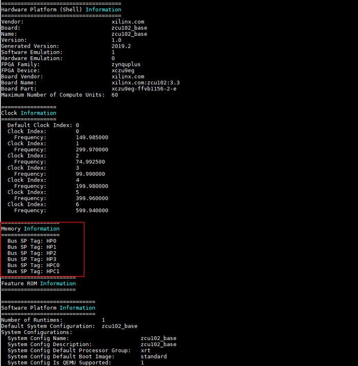
There are three clock domains in the DPUCZDX8G IP, associated with register configuration, the
DPU data plane and computation. The three input clocks can be configured independently in
order to match system and performance requirements. Therefore, the corresponding reset for the
three input clocks must be configured correctly.
Clock Domain
The following figure shows the three clock domains.
PG338 (v4.1) January 23, 2023 www.xilinx.com
Send Feedback
DPUCZDX8G for ZynqUltraScale+ MPSoCs 36Chapter 4: DPU Configuration
Figure 14: Clock Domains in the DPUCZDX8G
s_axi_clk Register
Configuration
Data Controller
m_axi_dpu_aclk
PL
dpu_2x_aclk
Calculation Unit
DPU
X22334-121020
Register Clock
s_axi_aclk is used for the register configuration module. This module receives the
DPUCZDX8G configuration though the S_AXI interface. The S_AXI clock can be common with
the M-AXI clock or an independent clock. The DPUCZDX8G configuration registers are updated
at a very low frequency and most of those registers are set only at the start of a task. Because
the M-AXI domain directly impacts DPU performance, Xilinx recommends that the user configure
the S-AXI is an independent clock with a frequency of 100MHz, while targeting a higher
frequency for the M-AXI clocks.
In the Vitis flow, the platform may provide only two clocks for the DPUCZDX8G IP. In this case,
the S_AXI clock must be configured as common with the M-AXI clock and target the higher
frequency.
Data Controller Clock
The primary function of the data controller module is to schedule the data flow in the
DPUCZDX8G IP. The data controller module is clocked from m_axi_dpu_aclk. Data transfer
between the DPUCZDX8G and external memory is clocked from the data controller clock
domain, thus, m_axi_dpu_aclk serves as a clock source for both the data controller and the
AXI_MM master interface. m_axi_dpu_aclk should be connected to the AXI_MM master
clock.
Computation Clock
The DSP slices in the computation unit module are in the dpu_2x_clk domain, which runs at
twice the clock frequency of the data controller module. The two related clocks must be edge-
aligned.
PG338 (v4.1) January 23, 2023 www.xilinx.com
Send Feedback
DPUCZDX8G for ZynqUltraScale+ MPSoCs 37You can also read