I.MX 8M Nano Hardware Developer's Guide - NXP ...
←
→
Page content transcription
If your browser does not render page correctly, please read the page content below
NXP Semiconductors             Document identifier: IMX8MNHDG
User's Guide                                   Rev. 1, 11/2020

i.MX 8M Nano Hardware Developer’s Guide
NXP Semiconductors

Contents
Chapter 1 Overview............................................................................................... 4
       1.1 Device supported.......................................................................................................................4
       1.2 Essential references.................................................................................................................. 4
       1.3 Supplementary references........................................................................................................ 4
       1.4 Related documentation..............................................................................................................5
       1.5 Conventions...............................................................................................................................5
       1.6 Acronyms and abbreviations..................................................................................................... 5

Chapter 2 i.MX 8M Nano design checklist............................................................. 8
       2.1 Design checklist table................................................................................................................8
       2.2 JTAG signal termination.......................................................................................................... 17
       2.3 Signal termination for Boundary-scan..................................................................................... 17

Chapter 3 i.MX 8M Nano layout/routing recommendations................................. 18
       3.1 Introduction..............................................................................................................................18
       3.2 Basic design recommendations...............................................................................................18
       3.3 Stack-up and manufacturing recommendations...................................................................... 18
       3.4 DDR design recommendations................................................................................................21
       3.5 Trace impedance recommendations....................................................................................... 53
       3.6 Power connectivity/routing.......................................................................................................54
       3.7 USB connectivity..................................................................................................................... 57
       3.8 Unused input/output terminations............................................................................................57

Chapter 4 Avoiding board bring-up problems...................................................... 59
       4.1 Introduction..............................................................................................................................59
       4.2 Avoiding power pitfalls -Current...............................................................................................59
       4.3 Avoiding power pitfalls -Voltage.............................................................................................. 59
       4.4 Checking for clock pitfalls........................................................................................................ 61
       4.5 Avoiding reset pitfalls...............................................................................................................61
       4.6 Sample board bring-up checklist............................................................................................. 61

Chapter 5 Using BSDL for Board-level Testing................................................... 64
       5.1 BSDL overview........................................................................................................................ 64
       5.2 How BSDL functions................................................................................................................64
       5.3 Downloading the BSDL file......................................................................................................64
       5.4 Pin coverage of BSDL............................................................................................................. 64
       5.5 Boundary scan operation.........................................................................................................64
       5.6 DDR4 connectivity test in Boundary-Scan...............................................................................67
       5.7 I/O pin power considerations................................................................................................... 68

Chapter 6 Thermal Considerations...................................................................... 69
       6.1 Introduction..............................................................................................................................69
       6.2 PCB Dimensions..................................................................................................................... 69
       6.3 Copper Volume........................................................................................................................69
       6.4 Thermal Resistance.................................................................................................................70
       6.5 Power Net Design....................................................................................................................70

                                         i.MX 8M Nano Hardware Developer’s Guide, Rev. 1, 11/2020
User's Guide                                                                                                                                    2 / 74
NXP Semiconductors
Contents
6.6 Component Placement............................................................................................................ 70
6.7 PCB Surroundings...................................................................................................................71
6.8 Thermal Simulations................................................................................................................71
6.9 Software optimization.............................................................................................................. 71
6.10 The Thermal Checklist...........................................................................................................72
Chapter 7 Revision history...................................................................................73
i.MX 8M Nano Hardware Developer’s Guide, Rev. 1, 11/2020
User's Guide 3 / 74NXP Semiconductors
Chapter 1
Overview
This document aims to help hardware engineers design and test the i.MX 8M Nano series processors. It provides examples on
board layout and design checklists to ensure first-pass success, and solutions to avoid board bring-up problems.
Engineers should understand board layouts and board hardware terminology.
This guide is released with relevant device-specific hardware documentation, such as datasheets, reference manuals, and
application notes. All these documents are available on i.MX 8M NANO.
1.1 Device supported
This document supports the i.MX 8M Nano (14 × 14 mm package).
1.2 Essential references
This guide is supplementary to the i.MX 8M Nano series chip reference manuals and data sheets. For reflow profile and thermal
limits during soldering, see General Soldering Temperature Process Guidelines (document AN3300). These documents are
available on i.MX 8M NANO.
1.3 Supplementary references
1.3.1 General information
The following documents introduce the Arm® processor architecture and computer architecture.
• For information about the Arm Cortex-A53 processor, see Cortex-A53
• For information about the Arm Cortex-M4F processor, see Cortex-M7
• Computer Architecture: A Quantitative Approach (Fourth Edition), by John L. Hennessy and David A. Patterson
• Computer Organization and Design: The Hardware/Software Interface (Second Edition), by David A. Patterson and John
L. Hennessy
The following documentation introduces the high-speed board design:
• Right the First Time- A Practical Handbook on High Speed PCB and System Design - Volumes I & II, by Lee W. Ritchey
(Speeding Edge) - ISBN 0-9741936- 0-72
• Signal and Power Integrity Simplified (2nd Edition), by Eric Bogatin (Prentice Hall)- ISBN 0-13- 703502-0
• High Speed Digital Design- A Handbook of Black Magic, by Howard W. Johnson & Martin Graham (Prentice Hall) - ISBN
0-13-395724-1
• High Speed Signal Propagation- Advanced Black Magic, by Howard W. Johnson & Martin Graham - (Prentice Hall) - ISBN
0-13-084408-X
• High Speed Digital System Design- A handbook of Interconnect Theory and Practice, by Hall, Hall and McCall (Wiley
Interscience 2000) - ISBN 0-36090-2
• Signal Integrity Issues and Printed Circuit Design, by Doug Brooks (Prentice Hall) ISBN 0-13- 141884-X
• PCB Design for Real-World EMI Control, by Bruce R. Archambeault (Kluwer Academic Publishers Group) - ISBN
1-4020-7130-2
• Digital Design for Interference Specifications - A Practical Handbook for EMI Suppression, by David L. Terrell & R.
Kenneth Keenan (Newnes Publishing) - ISBN 0-7506-7282-X
• Electromagnetic Compatibility Engineering, by Henry Ott (1st Edition - John Wiley and Sons) - ISBN 0-471-85068-3
i.MX 8M Nano Hardware Developer’s Guide, Rev. 1, 11/2020
User's Guide 4 / 74NXP Semiconductors
Overview
• Introduction to Electromagnetic Compatibility, by Clayton R. Paul (John Wiley and Sons) - ISBN 978-0-470-18930-6
• Grounding & Shielding Techniques, by Ralph Morrison (5th Edition - John Wiley & Sons) - ISBN 0- 471-24518-6
• EMC for Product Engineers, by Tim Williams (Newnes Publishing) - ISBN 0-7506- 2466-3
1.4 Related documentation
Additional literature will be published when new NXP products become available.
For the list of current documents, see i.MX 8M NANO.
1.5 Conventions
Table 1 lists the notational conventions used in this document.
Table 1. Conventions used in the document
Conventions Description
Courier Used to indicate commands, command parameters, code examples, and file and directory names.
Italics Used to indicates command or function parameters.
Bold Function names are written in bold.
cleared/set When a bit takes the value zero, it means to be cleared; when it takes a value of one, it means to be set.
mnemonics Instruction mnemonics are shown in lowercase bold. Book titles in text are set in italics.
sig_name Internal signals are written in all lowercase.
nnnn nnnnh Denotes hexadecimal number
0b Denotes binary number
rA, rB Instruction syntax used to identify a source GPR
rD Instruction syntax used to identify a destination GPR
REG[FIELD] Abbreviations for registers are shown in uppercase. Specific bits, fields, or ranges appear in brackets. For
example, MSR[LE] refers to the little-endian mode enable bit in the machine state register.
x An italicized x indicates an alphanumeric variable.
n, m An italicized n indicates a numeric variable.
In this guide, notation for all logical, bit-wise, arithmetic, comparison, and assignment operations follow C Language conventions.
1.6 Acronyms and abbreviations
Table 2 defines the acronyms and abbreviations used in this document.
i.MX 8M Nano Hardware Developer’s Guide, Rev. 1, 11/2020
User's Guide 5 / 74NXP Semiconductors
Overview
Table 2. Definitions and acronyms
Acronym Definition
ARMTM Advanced RISC Machines processor architecture
BGA Ball Grid Array package
BOM Bill of Materials
BSDL Boundary Scan Description Language
CAN Flexible Controller Area Network peripheral
CCM Clock Controller Module
CSI MIPI Camera Serial Interface
DDR Dual Data Rate DRAM
DDR3L Low voltage DDR3 DRAM
DDR4 DDR4 DRAM
DDRC DDR Controller
DFP Downstream Facing Port (USB Type-C)
DRP Dual Role Port (USB Type-C)
ECSPI Enhanced Configurable SPI peripheral
EIM External Interface Module
ENET 10/100/1000 Mbps Ethernet MAC peripheral
EPIT Enhanced Periodic Interrupt Timer peripheral
ESR Equivalent Series Resistance
GND Ground
GPC General Power Controller
GPIO General Purpose Input/Output
HDCP High-bandwidth Digital Content Protection
I2C Inter-integrated Circuit interface
IBIS Input output Buffer Information Specification
IOMUX i.MX 8M Nano chip-level I/O multiplexing
Table continues on the next page...
i.MX 8M Nano Hardware Developer’s Guide, Rev. 1, 11/2020
User's Guide 6 / 74NXP Semiconductors
Overview
Table 2. Definitions and acronyms (continued)
Acronym Definition
JTAG Joint Test Action Group
KPP Keypad Port Peripheral
LDB LVDS Display Bridge
LDO Low Drop-Out regulator
LPCG Low Power Clock Gating
LPDDR4 Low Power DDR4 DRAM
LVDS Low-Voltage Differential Signaling
MLB Media Local Bus
ODT On-Die Termination
OTP One-Time Programmable
PCB Printed Circuit Board
PCIe PCI Express
PCISig Peripheral Component Interconnect Special Interest Group
PDN Power Distribution Network
PMIC Power Management Integrated Circuit
POR Power-On Reset
PTH Plated Through Hole PCB (i.e. no microvias)
RGMII Reduced Gigabit Media Independent Interface (Ethernet)
RMII Reduced Media Independent Interface (Ethernet)
ROM Read-Only Memory
i.MX 8M Nano Hardware Developer’s Guide, Rev. 1, 11/2020
User's Guide 7 / 74NXP Semiconductors
Chapter 2
i.MX 8M Nano design checklist
This document provides a design checklist for the i.MX 8M Nano (14 x 14 mm package) processor. The design checklist tables
recommend optimal design and provide explanations to help users understand better. All supplemental tables referenced by the
checklist appear in sections following the design checklist tables.
2.1 Design checklist table
Table 3. LPDDR4 recommandations (i.MX 8M Nano)
Check box Recommendations Explanation/Supplemental recommendations
1. Connect the DRAM_ZN ball on the processor (ball This is a reference used during DRAM output
P2) to a 240 Ω, 1% resistor to GND. buffer driver calibration.
2. The ZQ0 and ZQ1 balls on the LPDDR4 device
should be connected through 240Ω, 1% resistors to the -
LPDDR4 VDD2 rail.
This will ensure adherence to the JEDEC
3. Place a 10 kΩ, 5% resistor to ground on the DRAM
specification until the control is configured and
reset signal.
starts driving the DDR.
LPDDR4 ODT on the i.MX 8M Nano is
4. The ODT_CA balls on the LPDDR4 device should be
command-based, making processor ODT_CA
connected directly to the LPDDR4 VDD2 rail.
output balls unnecessary.
5. The architecture for each chip inside the DRAM The processor does not support byte mode
package must be x 16. specified in JESD209-4B.
6. The processor ball MTEST (ball N2), should be left These are observability ports for manufacturing
unconnected. and are not used otherwise.
7. The VREF pin on the processor (ball P1) can be left The VREF signal for LPDDR4 is generated
unconnected. internally by the processor.
8. It is strongly suggested to use LPDDR4 if lower
The LPDDR4 can operate at low frequency
power consumption is required since DLL-off mode is
without DLL-off mode.
not supported.
9. VDD_DRAM should be always on during DDR
retention mode. Otherwise the data in DRAM might be See Errata e50381 for detailed information.
lost when exiting this mode.
Table 4. DDR4/DDR3L recommendations (i.MX 8M Nano)
Check box Recommendations Explanation/Supplemental recommendations
1. Connect the ZQ(DRAM_ZN) ball on the processor This is a reference used during DRAM output
(ball P2) to individual 240 Ω, 1% resistors to GND. buffer driver calibration.
Table continues on the next page...
i.MX 8M Nano Hardware Developer’s Guide, Rev. 1, 11/2020
User's Guide 8 / 74NXP Semiconductors
i.MX 8M Nano design checklist
Table 4. DDR4/DDR3L recommendations (i.MX 8M Nano) (continued)
Check box Recommendations Explanation/Supplemental recommendations
2. The ZQ ball on each DDR4/DDR3L device should
be connected through individual 240 Ω, 1% resistors to -
GND.
3. Place a 10 kΩ, 5% resistor to ground on the DRAM This will ensure adherence to the JEDEC
reset signal. specification until the control is configured and
starts driving the DDR.
4. The processor ball MTEST (ball N2), should be left These are observability ports for manufacturing
unconnected. and are not used otherwise.
5. Using x16 bit board to test the x8 bit DDR feature, Using x8 bit setting for initial and train on a x16 bit
only the controller setting is different, the PHY should board, it may cause some issues, such as:
train as x16 bit device.
• BG issue
• PDA(Per DRAM Accessibility) based train
issue.
6. DLL-off mode isn’t supported, which means DDR4/ The power consumption for low power mode in
DDR3L can’t run in low frequency such as 100MTS. DDR4/DDR3L system will be higher compared
with LPDDR4 system.
7. VDD_DRAM should be always on during DDR
retention mode. Otherwise the data in DRAM might be See Errata e50381 for detailed information.
lost when exiting this mode.
Table 5. I2C recommendations
Check box Recommendations Explanation/Supplemental recommendations
The I2C bus can only be operated as fast as the
slowest peripheral on the bus. If faster operation
1. Verify the target I2C interface clock rates
is required, move the slow devices to another
I2C port.
There are multiple I2C ports available on
chip, so if a conflict exists, move one of the
2. Verify that there are no I2C address conflicts on any
conflicting devices to a different I2C bus. If it
of the I2C buses utilized
is impossible, use a I2C bus switch (NXP part
number PCA9646).
This could result in excessive loading and
3. Do not place more than one set of pull-up resistors potential incorrect operation. Choose the pull-
on the I2C lines. up value commensurate with the bus speed
being used.
4. Ensure that the VCC rail powering the i.MX 8M Nano
Prevent device damage or incorrect operation due
I2C interface balls matches the supply voltage used for
2 to voltage mismatch.
the pull-up resistors and the slave I C devices.
i.MX 8M Nano Hardware Developer’s Guide, Rev. 1, 11/2020
User's Guide 9 / 74NXP Semiconductors
i.MX 8M Nano design checklist
Table 6. JTAG recommendations
Check box Recommendations Explanation/Supplemental recommendations
JTAG_TDO is configured with an on-chip
1. Do not use external pullup or pulldown resistors on
keeper circuit and the floating condition is
JTAG_TDO.
actively eliminated.
2. Follow the recommendations for external pull-up and -
pull-down resistors given in Table 17.
3. JTAG_MOD should be connected to ground through
-
a resistor.
4. JTAG_TMS pin must be connected with a 50ohm
series resistor near the component if used or fanout. -
Otherwise, floating if not fanout.
Table 7. Reset and ON/OFF recommendations
Check box Recommendations Explanation/Supplemental recommendations
POR_B is driven by the PMIC. If a reset button
1. The POR_B input must be asserted at powered up is used, it should be connected to the PWRON_B
and remain asserted until the last power rail for devices pin of the PMIC instead of directly connected
required for system boot are at their working voltage. to POR_B pin of the CPU. When POR_B is
This functionality is controlled by the PMIC on EVK. asserted (low) on the i.MX 8M Nano, the output
PMIC_ON_REQ remains asserted (high).
A brief connection to GND in OFF mode
causes the internal power management state
2. For portable applications, the ONOFF pin may be
machine to change state to ON. In ON mode,
connected to an ON/OFF SPST push-button switch to
a brief connection to GND generates an interrupt
ground. An external pull-up resistor is required on this
(intended to initiate a software-controllable power-
pin.
down). The connection to GND for approximate 5
seconds or more causes a forced OFF.
i.MX8M Nano can't be reset by internal reset
3. Connect GPIO1_IO02( WDOG_B, ball AG13) to
source in idle mode, repower is preferred. Some
external PMIC or reset IC to repower the system
peripherals like SD3.0, QSPI also need repower
except SNVS is strongly recommended.
during system reset.
During entering boundary scan mode, WDOG_B
4. GPIO1_IO02( WDOG_B, ball AG13) is used as Cold is always low. Without the WDOG timer
Reset. If using PMIC BD71850MWV, external WDOG buffer circuit, WDOG_B will repeatedly reset
timer buffer circuit is needed to support boundary-scan 8MNANOD4- EVK when entering boundary-scan
mode. mode. See section 5.5. Boundary scan operation
for more details.
i.MX 8M Nano Hardware Developer’s Guide, Rev. 1, 11/2020
User's Guide 10 / 74NXP Semiconductors
i.MX 8M Nano design checklist
Table 8. USB recommendations
Check box Recommendations Explanation/
Supplemental recommendations
1. The USB1_TXRTUNE (ball E19) -
must be connected with a 200 Ω, 1%
resistor to the ground.
The USB1_VBUS pin must not connect
2. The USB1_VBUS (ball F22) must directly to the 5V VBUS voltage. This pin
be connected with a 30K Ω, 1% series must be isolated by an external resistor
resistor to 5V VBUS power. (30K Ω, 1%) so that the USB1_VBUS pin
sees a lower voltage.
3. Route all USB differential signals with
-
90 Ω differential impedance.
4. ESD protection should be
implemented at the connector
This will prevent potential damages to
pins. Choose a low capacitance
board components from ESD.
device recommended for high-speed
interfaces.
Table 9. FlexSPI recommendations
Check box Recommendations Explanation/Supplemental recommendations
There are three modes for the internal sample
clock for FlexSPI read data:
• Dummy read strobe generated by FlexSPI
controller and looped back internally
(FlexSPIn_MCR0[RXCLKSRC] = 0x0), can
only reach 66Mhz operation frequency;
1. Read strobe(DQS) pad should be floated or with • Dummy read strobe generated by FlexSPI
a 10-18pF cap load to compensate SIO/SCK controller and looped back through the DQS
pins load for high speed running, if the memory pad(FlexSPIn_MCR0[RXCLKSRC] = 0x1),
device doesn't provide DQS. can reach 133Mhz operation frequency.
In this mode, this pin can be floated or
put some cap loads on board level to
compensate SIO/SCK pins load;
• Read strobe provided by memory
device and input from DQS pad
(FlexSPIn_MCR0[RXCLKSRC] = 0x3), can
reach 133Mhz operation frequency.
Table 10. Oscillator/Crystal recommendations
Check box Recommendations Explanation/Supplemental recommendations
1. Connect a 24 MHz crystal and a 510K Ω resistor
This crystal should have ESR not greater than 80
between 24M_XTALI and 24M_XTALO (balls B27 and
Ω, and be rated for a drive level of at least 180
C26).
Table continues on the next page...
i.MX 8M Nano Hardware Developer’s Guide, Rev. 1, 11/2020
User's Guide 11 / 74NXP Semiconductors
i.MX 8M Nano design checklist
Table 10. Oscillator/Crystal recommendations (continued)
Check box Recommendations Explanation/Supplemental recommendations
µW. Follow the manufacturer’s recommendation
for loading capacitance. Use short traces between
the crystal and the processor, with a ground
plane under the crystal, load capacitors, and
associated traces.
2. Use the 32.768 kHz clock generated by the The voltage level of this driving clock should not
PMIC to drive the i.MX 8M Nano RTC_XTALI input exceed the voltage of the NVCC_SNVS rail, or the
(ball A26), and connect RTC_XTALO (ball B25) to damage/malfunction may occur. The RTC signal
VDD_SNVS_0P8. should not be driven if the NVCC_SNVS supply
is OFF. It can lead to damage or malfunction.
For RTC VIL and VIH voltage levels, see the
latest i.MX 8M Nano datasheet available at
www.nxp.com/i.MX8MNANO.
Table 11. Temperature sensor recommendations
Check box Recommendations Explanation/Supplemental recommendations
1. The TSENSOR_RES_EXT (ball J24) must be This external resistor is used for temperature
connected with a 100K Ω, 1% resistor to GND. calibration, the wrong resistor value will result in
erroneous behavior for the temperature sensor.
Table 12. i.MX 8M Nano power/decoupling recommendations
Check box Recommendations Explanation/Supplemental recommendations
Any deviation from these sequences may result in
the following situations:
1. Comply with the power-up sequence guidelines • Excessive current during power-up phase
as described in the datasheet to guarantee reliable
operations of the device. • Prevention of the device from booting
• Irreversible damage to the processor (worst
case)
Common requirement for ripple noise peak-to-
2. Maximum ripple voltage requirements peak value should be less than 5% of the supply
voltage nominal value.
3. If using BD71850MWV PMIC to provide power,
Leaving any regulator except BUCK5/LDO4/
make sure all the regulators except BUCK5/LDO4/
LDO5 output open will lead to malfunction of
LDO5 have output L/C components properly
the PMIC.
connected, even if unused.
The voltage sensing pins are R_SNSP3_CFG,
4. If using PCA9450B PMIC to provide power, make
R_SNSPx and BUCKxFB in PCA9450B. Leaving
sure the voltage sensing pin of each BUCK is tied to
any BUCK output open, the PMIC will enter
VSYS if unused.
fault shutdown.
i.MX 8M Nano Hardware Developer’s Guide, Rev. 1, 11/2020
User's Guide 12 / 74NXP Semiconductors
i.MX 8M Nano design checklist
Table 13. Decoupling capacitors recommendations (i.MX 8M Nano)
Checkbox Supply 2.2 nF 0.22 µF 1 µF 4.7 µF 10 µF Notes
VDD_SOC, These 4 power rails are combined
together on EVK
VDD_DRAM,
- - 11 - 3
VDD_GPU,
VDD_DRAM_PLL_0P8
NVCC_DRAM - - 6 - 2 -
VDD_ARM - - 5 - 1 -
VDD_SNVS_0P8 - 1 - - - -
NVCC_SNVS_1P8 - - 1 - - -
VDD_24M_XTAL_1P8 - 1 - - - -
VDD_DRAM_PLL_1P8 - - 1 - - -
PVCC_1P8 - 2 - - - -
VDD_ARM_PLL_1P8,
VDD_ANA0_1P8,
VDD_ANA1_1P8, - 4 - - 1 -
VDD_USB_1P8,
VDD_MIPI_1P8
NVCC_SAI3,
NVCC_SAI5,
NVCC_ECSPI, - 4 - 1 - -
VDD_USB_3P3
NVCC_JTAG,
NVCC_NAND,
NVCC_SAI2,
NVCC_GPIO1, - 3 - - 1 -
NVCC_I2C,
NVCC_UART,
NVCC_SD1,
NVCC_CLK
NVCC_SD2 - 1 - - - -
NVCC_ENET - 1 - - - -
VDD_ARM_PLL_0P8, - 1 - 1 - -
Table continues on the next page...
i.MX 8M Nano Hardware Developer’s Guide, Rev. 1, 11/2020
User's Guide 13 / 74NXP Semiconductors
i.MX 8M Nano design checklist
Table 13. Decoupling capacitors recommendations (i.MX 8M Nano) (continued)
Checkbox Supply 2.2 nF 0.22 µF 1 µF 4.7 µF 10 µF Notes
VDD_ANA_0P8,
VDD_USB_0P8,
VDD_MIPI_1P2 - 1 - - - -
VDD_MIPI_0P8 - 1 - - - -
Must connect a 2.2nF capacitor
MIPI_VREG_CAP 1 - - - - between MIPI_VREG_CAP (ball
D15) and GND.
Capacitor part number used on EVK:
• 2.2 nF --- GRM033R71C222KA88D
• 0.22 uF --- LMK063BJ224MP-F
• 1 uF --- 02016D105MAT2A
• 4.7 uF --- CL05A475KP5NRNC
• 10 uF --- ZRB15XR60J106ME12D
Table 14. Bulk/Bypass capacitors recommendations ( ROHM BD71850MWV PMIC)
Checkbox Supply 1 µF 4.7 µF 10 µF 22 µF Notes
BUCK1 -
- - - 2
(VDD_SOC&DRAM&GPU)
BUCK2 -
- - - 2
(VDD_ARM)
BUCK6 -
- - - 2
(VDD_3V3)
BUCK7 -
- - - 2
(VDD_1V8)
BUCK8 -
- - - 2
(NVCC_DRAM)
LDO1 -
1 - - -
(NVCC_SNVS_1V8)
LDO2 -
1 - - -
(VDD_SNVS_0V8)
Table continues on the next page...
i.MX 8M Nano Hardware Developer’s Guide, Rev. 1, 11/2020
User's Guide 14 / 74NXP Semiconductors
i.MX 8M Nano design checklist
Table 14. Bulk/Bypass capacitors recommendations ( ROHM BD71850MWV PMIC) (continued)
Checkbox Supply 1 µF 4.7 µF 10 µF 22 µF Notes
LDO3
- 1 - - -
(VDDA_1V8)
LDO6
- 1 - - -
(VDD_PHY_1V2)
MUXSW_VOUT
- - 1 - -
(NVCC_SD2)
Capacitor part number used on EVK:
• 1 uF --- 02016D105MAT2A
• 4.7 uF --- CL05A475KP5NRNC
• 10 uF --- GRM188R61A106KE69D
• 22 uF --- C1608X5R1A226M080AC
Table 15. Bulk/Bypass capacitors recommendations (NXP PCA9450B PMIC)
Checkbox Supply 1 µF 2.2 µF 22 µF Notes
BUCK1
- - 1
(VDD_SOC&DRAM&GPU)
BUCK2 -
- - 1
(VDD_ARM)
BUCK4 -
- - 1
(VDD_3V3)
BUCK5 -
- - 1
(VDD_1V8)
BUCK6 -
- - 1
(NVCC_DRAM)
LDO1 -
1 - -
(NVCC_SNVS_1V8)
LDO2 -
1 - -
(VDD_SNVS_0V8)
LDO3
- 1 - -
(VDDA_1V8)
Table continues on the next page...
i.MX 8M Nano Hardware Developer’s Guide, Rev. 1, 11/2020
User's Guide 15 / 74NXP Semiconductors
i.MX 8M Nano design checklist
Table 15. Bulk/Bypass capacitors recommendations (NXP PCA9450B PMIC) (continued)
Checkbox Supply 1 µF 2.2 µF 22 µF Notes
LDO4
1 - - -
(VDD_PHY_1V2)
LDO5
1 - - -
(NVCC_SD2)
Capacitor part number used on EVK:
• 1 uF --- 02016D105MAT2A
• 2.2 uF --- C1005X5R1A225K
• 22 uF --- C1608X5R1A226M080AC
Table 16. PCB design recommendations
Check box Recommendations Explanation/Supplemental recommendations
Controlled impedance is the key factor to have good
signal integrity. Note that the reference plane can
only be GND or the signal’s own I/O power. Do not
1. High-speed signal traces have reference plane in use other nets as reference.
adjacent layer and are impedance controlled.
For DRAM, only GND reference is accepted for
maintaining impedance. The power plane reference
can’t be as the sole impedance return.
2. High-speed signal traces never cross gap or slot Crossing gap in reference plane will cause reflection
in reference plane. and increase crosstalk.
3. Place at least one GND stitching via within 50 mils GND stitching via can help keep impedance
of signal via when switching reference planes. continuous and reduce via crosstalk.
4. Appropriate delay matching is done for parallel Signals within a bus should have delay time matched
bus. to maintain timing margin.
5. The true and complementary signal of a The true and complementary signal within
differential pair must have delay matched to within a differential pair should have delay time
1ps. tightly matched.
6. DDR interface passed SI simulation. Alternatively, Generally, SI simulation should be performed for
directly copy the EVK DDR layout design. DDR interface that runs at 3200 MT/s(LPDDR4) or
2400MT/s(DDR4) or 1600MT/s(DDR3L) to ensure
stable working. If this is not feasible, just copy the
EVK DDR layout design as well as the board stack-
up.
7. Place test point on key signals to ease debugging. Test points can bring excessive capacitance
When placing test point on high-speed signal traces, and should be carefully handled on high-speed
make sure its diameter is no more than 20mil and signal traces.
Table continues on the next page...
i.MX 8M Nano Hardware Developer’s Guide, Rev. 1, 11/2020
User's Guide 16 / 74NXP Semiconductors
i.MX 8M Nano design checklist
Table 16. PCB design recommendations (continued)
Check box Recommendations Explanation/Supplemental recommendations
the test point be directly placed on the trace with no
stub.
8. Decoupling capacitors are placed as close to IC Tight routing to both power and ground is needed to
power pins and GND pins as possible. provide optimum decoupling effectiveness.
2.2 JTAG signal termination
Table 17 is a JTAG termination chart showing what terminations should be placed on PCB designs.
Table 17. Recommended JTAG board terminations
JTAG signal I/O type External termination Comments
JTAG_TCK Input 10 kΩ pull-down -
JTAG_TMS Input 50ohm serial resistor Internal pulled up to NVCC_JTAG, connected
with a 50ohm serial resistor.
JTAG_TDI Input None Internal pulled up to NVCC_JTAG, no external
termination required
JTAG_TDO 3-state output None -
2.3 Signal termination for Boundary-scan
Table 18 is a signal termination chart showing what terminations should be placed on board designs to support Boundary-scan.
Table 18. Recommended board terminations for Boundary-scan
JTAG signal I/O type External termination Comments
BOOT_MODE0 Input Pull up BOOT_MODE[3:0] must be at 1111 before
entering Boundary-scan mode.
BOOT_MODE1 Input Pull up
BOOT_MODE2 Input Pull up
BOOT_MODE3 Input Pull up
POR_B Input Pull up
RTC_RESET_B Input Pull up If using PMIC PCA9450B, it is internally
pulled up.
i.MX 8M Nano Hardware Developer’s Guide, Rev. 1, 11/2020
User's Guide 17 / 74NXP Semiconductors
Chapter 3
i.MX 8M Nano layout/routing recommendations
3.1 Introduction
This chapter describes how to assist design engineers with the layout of an i.MX 8M Nano-based system.
3.2 Basic design recommendations
When using the Allegro design tool, the schematic symbol & PCB footprint created by NXP is recommended. When not using the
Allegro tool, use the Allegro footprint export feature (supported by many tools). If the export is not possible, create the footprint
per the package dimensions outlined in the product data sheet.
Native Allegro layout and gerber files are available on i.MX 8M NANO EVK.
3.2.1 Placing decoupling capacitors
Place small decoupling and larger bulk capacitors on the bottom side of the PCB.
The 0201 or 0402 decoupling and 0603 or larger bulk capacitors should be mounted as close as possible to the power vias. The
distance should be less than 50 mils. Additional bulk capacitors can be placed near the edge of the BGA via array. Placing the
decoupling capacitors close to the power balls is critical to minimize inductance and ensure high-speed transient current required
by the processor. See the i.MX 8M Nano EVK layouts for examples of the desired decoupling capacitor placement.
The following list describes how to choose correct decoupling scheme:
• Place the largest capacitance in the smallest package that budget and manufacturing can support.
• For high-speed bypassing, select the required capacitance with the smallest package (for example, 0.1 μF, 0.22 μF, 1.0
μF, or even 2.2 μF in a 0201 package size).
• Minimize trace length (inductance) to small caps.
• Series inductance cancels out capacitance.
• Tie caps to GND plane directly with a via.
• Place capacitors close to the power ball of the associated package from the schematic.
• A preferred BGA power decoupling design is available on the EVK board design available on i.MX 8M NANO EVK.
Customers should use the NXP design strategy for power and decoupling.
3.3 Stack-up and manufacturing recommendations
3.3.1 Stack-up recommendation (i.MX 8M Nano)
Due to the number of balls on the i.MX 8M Nano processor in the 14 mm x 14 mm package, a minimum 6-layer PCB stack-up is
recommended. For the 6-layers on the PCB, a sufficient number of layers need to be dedicated to power on routing to meet the
IR drop target of 2% for the i.MX 8M Nano CPU power rails.
The constraints for the trace width will depend on such factors as the board stack-up and associated dielectric and copper
thickness, required impedance, and required current (for power traces). The stack-up also determines the constraints for routing
and spacing. Consider the following requirements when designing the stack-up and selecting board material:
• Board stack-up is critical for high-speed signal quality.
• Preplanning impedance of critical traces is required.
• High-speed signals must have reference planes on adjacent layers to minimize cross-talk.
i.MX 8M Nano Hardware Developer’s Guide, Rev. 1, 11/2020
User's Guide 18 / 74NXP Semiconductors
i.MX 8M Nano layout/routing recommendations
• PCB material: the material used on EVK is TU768.
3.3.2 Manufacturing recommendation (i.MX 8M Nano)
Since the i.MX 8M Nano processor uses 0.5mm-pitch BGA package, the PCB technology must meet below requirement to fully
fanout all the signals of the processor using PTH(plated through holes).
• Minimum trace width: 3.2mil
• Minimum trace to trace/pad spacing: 3.2mil
• Minimum via size: 8mil-diameter hole, 16mil-diameter pad
• Minimum via pad to pad spacing: 4mil
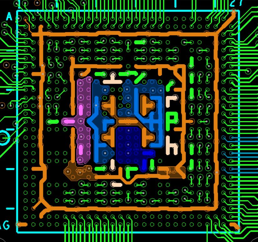
Figure 1 shows the reference routing of the i.MX 8M Nano, PTH is ok for the fanout, HDI is not needed.
Figure 1. i.MX 8M Nano fanout routing on EVK
i.MX 8M Nano Hardware Developer’s Guide, Rev. 1, 11/2020
User's Guide 19 / 74NXP Semiconductors
i.MX 8M Nano layout/routing recommendations
3.3.3 EVK PCB stack-up (i.MX 8M Nano)
Table 19 and Table 20 show stack-up of the LPDDR4 EVK. The LPDDR4 CPU board use 6-layer stack-up and the BB board use
8-layer stack-up. DDR4 and shares same BB board as 8MMINI-BB, and CPU board stack-up is similar, users can also use similar
stack-up, but need to confirm with PCB manufacturer.
Table 19. 8MNANOLPD4-CPU Board stack up information
Layer Description Copper (Oz.) Dielectric thickness (mil)
1 Signal 0.5+Plating
Dielectric 2.76 mil
2 GND 1
Dielectric 2.95 mil
3 Signal 1
Dielectric 25.28 mil
4 Power 1
Dielectric 2.95 mil
5 Power 1
Dielectric 2.76 mil
6 Signal 0.5+Plating
Total thickness: 47.24(4.72/-4.72) mil 1.2(+0.12/-0.12) MM
Material: TU768 TU768
Table 20. 8MMINI-BB Board stack up information
Layer Description Copper (Oz.) Dielectric thickness (mil)
1 Signal 0.5+Plating
Dielectric 2.717 mil
2 GND 1
Dielectric 4.33 mil
3 Signal 1
Dielectric 11.085 mil
4 Power 1
Table continues on the next page...
i.MX 8M Nano Hardware Developer’s Guide, Rev. 1, 11/2020
User's Guide 20 / 74NXP Semiconductors
i.MX 8M Nano layout/routing recommendations
Table 20. 8MMINI-BB Board stack up information (continued)
Layer Description Copper (Oz.) Dielectric thickness (mil)
Dielectric 14.170 mil
5 Power 1
Dielectric 11.415 mil
6 Signal 1
Dielectric 4.33 mil
7 GND 1
Dielectric 2.717 mil
8 Signal 0.5+Plating
Total thickness: 62.992(6.299/-6.299) mil 1.6(+0.16/-0.16) MM
Material: TU768 TU768
3.4 DDR design recommendations
3.4.1 DDR connection information
The i.MX 8M Nano processor can be used with LPDDR4, DDR4 or DDR3L memory. Since these memory types have different I/O
signals, there are 38 generically-named functional balls, depending on the type of memory used. See Table 21 for the connectivity
of these generic balls for DDR3L, LPDDR4 and DDR4. The schematic symbol created by NXP already replaced these generic
names with DDR function.
Table 21. DDR3L/LPDDR4/DDR4 ADD/CMD/CTRL signals connectivity
Ball name Ball # LPDDR4 function DDR4 function DDR3L function
DRAM_AC00 F4 CKE0_A CKE0 CKE0
DRAM_AC01 F5 CKE1_A CKE1 CKE1
DRAM_AC02 K4 CS0_A CS0_n CS0#
DRAM_AC03 J4 CS1_A C0 -
DRAM_AC04 L2 CK_t_A BG0 BA2
DRAM_AC05 L1 CK_c_A BG1 A14
DRAM_AC06 F6 - ACT_n A15
DRAM_AC07 J5 - A9 A9
Table continues on the next page...
i.MX 8M Nano Hardware Developer’s Guide, Rev. 1, 11/2020
User's Guide 21 / 74NXP Semiconductors
i.MX 8M Nano layout/routing recommendations
Table 21. DDR3L/LPDDR4/DDR4 ADD/CMD/CTRL signals connectivity (continued)
Ball name Ball # LPDDR4 function DDR4 function DDR3L function
DRAM_AC08 J6 CA0_A A12 A12/BC#
DRAM_AC09 K6 CA1_A A11 A11
DRAM_AC10 E4 CA2_A A7 A7
DRAM_AC11 D5 CA3_A A8 A8
DRAM_AC12 N4 CA4_A A6 A6
DRAM_AC13 N5 CA5_A A5 A5
DRAM_AC14 K5 - A4 A4
DRAM_AC15 N6 - A3 A3
DRAM_AC16 M1 - CK_t_A CK_A
DRAM_AC17 M2 - CK_c_A CK#_A
DRAM_AC19 N2 MTEST MTEST MTEST
DRAM_AC20 AB4 CKE0_B CK_t_B CK_B
DRAM_AC21 AB5 CKE1_B CK_c_B CK#_B
DRAM_AC22 W4 CS1_B - -
DRAM_AC23 V4 CS0_B - -
DRAM_AC24 U2 CK_t_B A2 A2
DRAM_AC25 U1 CK_c_B A1 A1
DRAM_AC26 N1 - BA1 BA1
DRAM_AC27 R6 - PARITY -
DRAM_AC28 W6 CA0_B A13 A13
DRAM_AC29 V6 CA1_B BA0 BA0
DRAM_AC30 AC4 CA2_B A10 / AP A10 / AP
DRAM_AC31 AD5 CA3_B A0 A0
DRAM_AC32 R4 CA4_B C2 -
DRAM_AC33 R5 CA5_B CAS_n / A15 CAS#
Table continues on the next page...
i.MX 8M Nano Hardware Developer’s Guide, Rev. 1, 11/2020
User's Guide 22 / 74NXP Semiconductors
i.MX 8M Nano layout/routing recommendations
Table 21. DDR3L/LPDDR4/DDR4 ADD/CMD/CTRL signals connectivity (continued)
Ball name Ball # LPDDR4 function DDR4 function DDR3L function
DRAM_AC34 T1 - WE_n / A14 WE#
DRAM_AC35 T2 - RAS_n / A16 RAS#
DRAM_AC36 V5 - ODT0 ODT0
DRAM_AC37 W5 - ODT1 ODT1
DRAM_AC38 AB6 - CS1_n CS1#
3.4.2 LPDDR4-3200 design recommendations
The following list details some generic guidelines that should be adhered to when implementing an i.MX 8M Nano design
using LPDDR4.
1. It is expected that the layout engineer and design team already h ave experience and training with DDR designs at
speeds of 1.6 GHz / 3200 MT/s.
2. All high-speed signal traces must reference a solid GND plane. Referencing only to the VDD power plane is not
supported.
3. Keep edge to edge spacing of high speed signal traces no less than 2 times the trace width to minimize trace crosstalk.
Increase spacing when available in the system.
4. At a speed of 3200 MT/s, signal vias can be a significant source of crosstalk. If not properly designed, they can
introduce crosstalk larger than that from the trace. To minimize via crosstalk, make sure the total number of vias to be
two or less on each point-to-point single-ended/differential trace. Place at least one ground stitching via within 50 mils of
signal via when switching reference planes to provide continuous return path and reduce crosstalk. If it is not possible to
place enough ground stitching vias due to space limitation, try to make the length that the signal actually travels on the
via as short as possible, as illustrated in Figure 2.
i.MX 8M Nano Hardware Developer’s Guide, Rev. 1, 11/2020
User's Guide 23 / 74NXP Semiconductors
i.MX 8M Nano layout/routing recommendations
Figure 2. Length that the signal actually travels on the Via
5. CLK and DQS signals can be routed on different layer with DQ/CA signals to ease routing. When doing this, keep no
less than 5 times trace width spacing from other signals.
6. U se time delay instead of length when performing the delay matching. The delay matching includes the PCB trace
delay and the IC package delay. Incorporate the package pin delay into the CAD tool’s constraint manager.
7. Include the delay of vias when performing delay matching. This can be realized in Allegro tool by enabling the Z Axis
Delay in “Setup -> Constraints -> Modes”.
8. Data Byte swapping within each 16-bit channel is OK. Bit swapping within each slice/byte lane is OK.
9. Bit swapping of Command/Address (CA[5:0], CKE[1:0], CS[1:0]) signals is NOT allowed.
10. i.MX 8M Nano does not drive ODT_CA signal. The ODT_CA balls on the LPDDR4 devices should be connected
directly to the VDD2 supply.
11. In general, the 200-ball LPDDR4 package should be placed 200 mils from the i.MX 8M Nano .
12. Enable the DBI (data bus inversion) feature. It can help reduce both power consumption and power noise.
13. The LPDDR4 routing delay rules allow for reduction of most DATA bus serpentine requirements resulting in easier
routing on i.MX 8M Nano. Command Bus Training is required for LPDDR4. Please ensure SW enables and configures
the Command Bus Training.
14. The LPDDR4 routing delay rules allow for limited reduction Command/Address bus serpentine requirements on i.MX
8M Nano. Address/Command Bus is sectioned into 3 group that still require tight timing control. Command Bus
Training is required for LPDDR4. Please ensure SW enables and configures the Command Bus Training.
3.4.2.1 i.MX 8M Nano LPDDR4-3200 routing recommendations
LPDDR4-3200 needs to be routed with signal fly times matched shown in Table 22. The delay of the via transitions needs to
be included in the overall calculation. This can be realized in Allegro tool by enabling the Z Axis Delay in Setup -> Constraints
-> Modes.
i.MX 8M Nano Hardware Developer’s Guide, Rev. 1, 11/2020
User's Guide 24 / 74NXP Semiconductors
i.MX 8M Nano layout/routing recommendations
An example of the delay match calculation has been shown for the i.MX 8M Nano EVK board design in Table 23 and Table 24.
This analysis was done for the LPDDR4-3200 implementation using the i.MX 8M Nano. In Table 23 and Table 24, the PCB Delay
column was obtained directly from the Allegro PCB file, and the Pkg Delay column is the package delay obtained from Table 32.
NXP recommends that users simulate their LPDDR4 implementation before fabricating PCBs.
Table 22. i.MX 8M Nano LPDDR4-3200 routing recommendations
LPDDR4-3200
LPDDR4 signal (each Group PCB + package prop delay
16-bit channel)
Min Max Considerations
Match the true/
CK_t/CK_c Clock Short as possible 200 ps complement signals
within 1 ps.
Match CA5, CA4 within
CA5, CA4
2.0ps
Address/ Command/ Match CA3, CA2, CA1,
CA3, CA2, CA1, CA0 CK_t - 50 ps CK_t + 50 ps
Control CA0 within 2.0ps
CKE1, CKE0, CS1, Match CKE1, CKE0,
CS0 CS1, CS0 within 2.0ps
DQS0_t/DQS0_c Byte 0 - DQS CK_t - 75 ps CK_t + 75 ps
DM0
Byte 0 - Data DQS0_t -50 ps DQS0_t +50 ps
DQ[7:0] Match the true/
complement signals of
DQS1_t/DQS1_c Byte 1 - DQS CK_t - 75 ps CK_t + 75 ps each DQS within 1 ps.
DM1
Byte 1 - Data DQS1_t -50 ps DQS1_t +50 ps
DQ[15:8]
Table 23. LPDDR4 delay matching example (CA/CTL signals)
Net name PCB delay (ps) Pkg delay (ps) Comments
DRAM_CK_T_A 99 41.1 Vias are L1-> L6->L1
140.1 Total Net Delay
DRAM_CK_C_A 98.5 41.2 Vias are L1-> L6->L1
139.7 Total Net Delay
DRAM_CA0_A 134.2 39.6 Vias are L1-> L3->L1
173.8 Total Net Delay
DRAM_CA1_A 144.9 29.1 Vias are L1-> L3->L1
174 Total Net Delay
DRAM_CA2_A 119.6 54.8 Vias are L1-> L6->L1
174.4 Total Net Delay
DRAM_CA3_A 114 59.7 Vias are L1-> L6->L1
Table continues on the next page...
i.MX 8M Nano Hardware Developer’s Guide, Rev. 1, 11/2020
User's Guide 25 / 74NXP Semiconductors
i.MX 8M Nano layout/routing recommendations
Table 23. LPDDR4 delay matching example (CA/CTL signals) (continued)
Net name PCB delay (ps) Pkg delay (ps) Comments
173.7 Total Net Delay
DRAM_CA4_A 75.5 33.8 Vias are L1-> L3->L1
109.3 Total Net Delay
DRAM_CA5_A 78.2 32.0 Vias are L1-> L3->L1
110.2 Total Net Delay
DRAM_nCS0_A 142.8 35.9 Vias are L1-> L3->L1
178.7 Total Net Delay
DRAM_nCS1_A 134 44.2 Vias are L1-> L3->L1
178.2 Total Net Delay
DRAM_CKE0_A 127 51.2 Vias are L1-> L3->L1
178.2 Total Net Delay
DRAM_CKE1_A 138.9 39.9 Vias are L1-> L3->L1
178.8 Total Net Delay
Table 24. LPDDR4 length matching example (Byte0/Byte1 signals)
Net name PCB delay (ps) Pkg delay (ps) Comments
DRAM_SDQS0_T 122.6 59.0 Routed on bottom layer, no
via
181.6 Total Net Delay
DRAM_SDQS0_C 123.2 58.9 Routed on bottom layer, no
via
182.1 Total Net Delay
DRAM_DMI0 135.9 57.2 Vias are L1-> L3->L1
193.1 Total Net Delay
DRAM_DQ00 142.2 47.2 Vias are L1-> L3->L1
189.4 Total Net Delay
DRAM_DQ01 143.8 43.0 Vias are L1-> L3->L1
186.8 Total Net Delay
DRAM_DQ02 126.8 54.6 Vias are L1-> L3->L1
181.4 Total Net Delay
DRAM_DQ03 118.7 51.7 Vias are L1-> L3->L1
170.4 Total Net Delay
DRAM_DQ04 112.7 59.9 Vias are L1-> L3->L1
172.6 Total Net Delay
Table continues on the next page...
i.MX 8M Nano Hardware Developer’s Guide, Rev. 1, 11/2020
User's Guide 26 / 74NXP Semiconductors
i.MX 8M Nano layout/routing recommendations
Table 24. LPDDR4 length matching example (Byte0/Byte1 signals) (continued)
Net name PCB delay (ps) Pkg delay (ps) Comments
DRAM_DQ05 114.8 58.1 Vias are L1-> L3->L1
172.9 Total Net Delay
DRAM_DQ06 114 64.6 Vias are L1-> L3->L1
178.6 Total Net Delay
DRAM_DQ07 126.6 51.4 Vias are L1-> L3->L1
178 Total Net Delay
DRAM_SDQS1_T 83.5 48.6 Routed on bottom layer, no
via
132.1 Total Net Delay
DRAM_SDQS1_C 84.2 47.2 Routed on bottom layer, no
via
131.4 Total Net Delay
DRAM_DMI1 56.8 58.6 Routed on top layer, no via
115.4 Total Net Delay
DRAM_DQ008 56.1 45.0 Routed on top layer, no via
101.1 Total Net Delay
DRAM_DQ09 53.5 50.1 Routed on top layer, no via
103.6 Total Net Delay
DRAM_DQ10 55.8 46.2 Routed on top layer, no via
103 Total Net Delay
DRAM_DQ11 52.3 47.2 Routed on top layer, no via
99.5 Total Net Delay
DRAM_DQ12 50 40.3 Routed on top layer, no via
90.3 Total Net Delay
DRAM_DQ13 71.5 48.8 Routed on top layer, no via
120.3 Total Net Delay
DRAM_DQ14 67.3 58.4 Routed on top layer, no via
125.7 Total Net Delay
DRAM_DQ15 78.2 52.4 Routed on top layer, no via
130.6 Total Net Delay
3.4.2.2 LPDDR4-3200 routing example (i.MX 8M Nano)
Figure 3 to Figure 5 show the placement and routing of the LPDDR4 signals on the i.MX 8M Nano EVK board. The CLK and DQS
signals are routed on bottom layer to save routing space on top layer and layer 3. Data byte lane 1 signals are routed on top layer,
and data byte lane 0 and CA/CTL signals are routed on layer 3. This is to make the signal actually travels on the via as short as
possible to minimize via crosstalk.
i.MX 8M Nano Hardware Developer’s Guide, Rev. 1, 11/2020
User's Guide 27 / 74NXP Semiconductors
i.MX 8M Nano layout/routing recommendations
Figure 3. i.MX 8M Nano EVK board LPDDR4 routing (Top Layer)
i.MX 8M Nano Hardware Developer’s Guide, Rev. 1, 11/2020
User's Guide 28 / 74NXP Semiconductors
i.MX 8M Nano layout/routing recommendations
Figure 4. i.MX 8M Nano EVK board LPDDR4 routing (Layer 3)
i.MX 8M Nano Hardware Developer’s Guide, Rev. 1, 11/2020
User's Guide 29 / 74NXP Semiconductors
i.MX 8M Nano layout/routing recommendations
Figure 5. i.MX 8M Nano EVK board LPDDR4 routing (Bottom Layer)
3.4.3 i.MX 8M Nano DDR4-2400 design recommendations
The following list provides some generic guidelines for implementing an i.MX 8M Nano design using DDR4.
1. It is expected that the layout engineer and design team already has experience and training with DDR designs at
speeds of 1.2 GHz / 2400 MT/s.
2. DQ/DMI signal traces must refer to solid GND plane only. Addr/Cmd/Ctrl signal traces can refer to GND plane only or
GND+VDDQ plane (when routed as strip line). Referring to VDDQ plane only is not allowed.
3. Keep edge-to-edge spacing of high-speed signal traces no less than 1.5 times the trace width to minimize trace
crosstalk.
4. At a speed of 2400 MT/s, signal vias can be a significant source of crosstalk. If not properly designed, it can introduce
crosstalk larger than that from the trace. To minimize via crosstalk, make sure that the number of vias on each
point-to-point signal is no more than 2. Place at least one ground stitching via within 50 mils of signal via when switching
reference planes to provide continuous return path and reduce crosstalk. If it is not possible to place enough ground
stitching vias due to space limitation, try to make the length that the signal actually travels on the via as short as
possible, as illustrated in Figure 6.
i.MX 8M Nano Hardware Developer’s Guide, Rev. 1, 11/2020
User's Guide 30 / 74NXP Semiconductors
i.MX 8M Nano layout/routing recommendations
Figure 6. Length that the signal actually travels on the Via
5. CLK and DQS signals can be routed on different layers with DQ/CA signals to ease routing. When doing this, keep no
less than 5 times trace width spacing from other signals.
6. Use time delay instead of length when performing the delay matching. The delay matching includes the PCB trace delay
and the IC package delay. Incorporate the package pin delay into the CAD tool’s constraint manager.
7. Include the delay of vias when performing delay matching. This can be realized in Allegro tool by enabling the Z Axis
Delay in Setup -> Constraints -> Modes.
8. Data Byte swapping between upper/lower byte lane is allowed. Bit swapping within each slice/byte lane is allowed.
9. Bit swapping of Cmd/Addr/Ctrl signals is NOT allowed.
10. In general, the DDR4 DRAM should be placed 200 mils from the i.MX 8M Nano.
11. Enable the Data Bus Inversion (DBI) feature. It can help reduce both power consumption and power noise.
3.4.3.1 i.MX 8M Nano DDR4-2400 routing recommendations
DDR4-2400 needs to be routed with signal fly times matched shown in Table 25. The delay of the via transitions needs to be
included in the overall calculation. This can be realized in Allegro tool by enabling the Z Axis Delay in Setup -> Constraints
-> Modes.
An example of the delay match calculation has been shown for the i.MX 8M Nano DDR4 EVK board design in Table 26 and Table
27. This analysis is done for the DDR4-2400 implementation using the i.MX 8M Nano. In Table 26 and Table 27, the PCB Delay
column is obtained directly from the Allegro PCB file, and the Pkg Delay column is the package delay obtained from Table 32.
i.MX 8M Nano Hardware Developer’s Guide, Rev. 1, 11/2020
User's Guide 31 / 74NXP Semiconductors
i.MX 8M Nano layout/routing recommendations
Table 25. i.MX 8M Nano DDR4-2400 routing recommendations
DDR4-2400
PCB + package prop delay
DDR4/DDR3L signal Group Considerations
Min. Max.
Match the
CK_t/CK_c Clock Short as possible 500ps1 true/complement
signals within 1 ps.
A[13:0]/BA[1:0]/BG0
CS/RAS/WE/CAS Address/ Command/ Control CK_t - 10 ps CK_t + 10 ps
CKE/ODT
DQS0_t/DQS0_c Byte 0 - DQS Short as possible CK_t + 1.0 * tCK Match the
true/complement
DM0 signals of DQS
Byte 0 - Data DQS0_t -10 ps DQS0_t +10 ps within 1 ps.
DQ[7:0]
DQS1_t/DQS1_c Byte 1 - DQS Short as possible CK_t + 1.0 * tCK
DM1
Byte 1 - Data DQS1_t -10 ps DQS1_t + 10 ps
DQ[15:8]
1. For 16-bit single chip routed with point to point, CK_t/CK_c should be short as possible and much less than 500 ps. 230 ps
is recommended.
Table 26. DDR4 delay matching example (Addr/Cmd/Ctrl/CK signals)
Net name PCB delay (ps) Pkg delay (ps) Comment
167.2 56.5 Routed on top layer, no via
DRAM_A0
223.7 Total Net Delay
183.2 42.2 Routed on top layer, no via
DRAM_A1
225.4 Total Net Delay
181.1 41.8 Vias are L1-> L3->L1
DRAM_A2
222.9 Total Net Delay
202.7 22.4 Vias are L1-> L3->L1
DRAM_A3
225.1 Total Net Delay
DRAM_A4 179.9 43.1 Vias are L1-> L3->L1
Table continues on the next page...
i.MX 8M Nano Hardware Developer’s Guide, Rev. 1, 11/2020
User's Guide 32 / 74NXP Semiconductors
i.MX 8M Nano layout/routing recommendations
Table 26. DDR4 delay matching example (Addr/Cmd/Ctrl/CK signals) (continued)
Net name PCB delay (ps) Pkg delay (ps) Comment
223.0 Total Net Delay
191.9 32.0 Vias are L1-> L3->L1
DRAM_A5
223.9 Total Net Delay
189.1 33.8 Vias are L1-> L3->L1
DRAM_A6
222.9 Total Net Delay
167.2 54.8 Vias are L1-> L6->L1
DRAM_A7
222.0 Total Net Delay
165.9 59.7 Vias are L1-> L6->L1
DRAM_A8
225.6 Total Net Delay
189.4 35.8 Vias are L1-> L6->L1
DRAM_A9
225.2 Total Net Delay
165.6 59.5 Routed on top layer, no via
DRAM_A10
225.1 Total Net Delay
193.7 29.1 Vias are L1-> L3->L1
DRAM_A11
222.8 Total Net Delay
185.8 39.6 Vias are L1-> L6->L1
DRAM_A12
225.4 Total Net Delay
193.5 31.9 Routed on top layer, no via
DRAM_A13
225.4 Total Net Delay
188.4 34.4 Vias are L1-> L3->L1
DRAM_BA0
222.8 Total Net Delay
168.3 53.4 Vias are L1-> L3>L1
DRAM_BA1
221.7 Total Net Delay
183.8 41.1 Vias are L1-> L3>L1
DRAM_BG0
224.9 Total Net Delay
Table continues on the next page...
i.MX 8M Nano Hardware Developer’s Guide, Rev. 1, 11/2020
User's Guide 33 / 74NXP Semiconductors
i.MX 8M Nano layout/routing recommendations
Table 26. DDR4 delay matching example (Addr/Cmd/Ctrl/CK signals) (continued)
Net name PCB delay (ps) Pkg delay (ps) Comment
183.7 39.4 Vias are L1-> L6>L1
DRAM_CK_C
223.1 Total Net Delay
184.5 39.1 Vias are L1-> L6>L1
DRAM_CK_T
223.6 Total Net Delay
176.2 45.7 Vias are L1-> L6-> L1
DRAM_NACT
221.9 Total Net Delay
186.3 36.0 Vias are L1-> L3>L1
DRAM_NALERT
222.3 Total Net Delay
183.1 38.6 Vias are L1-> L6-> L1
DRAM_NCAS(A15)
221.7 Total Net Delay
171.6 51.2 Vias are L1-> L3->L1
DRAM_CKE
222.8 Total Net Delay
186.9 35.9 Vias are L1-> L3->L1
DRAM_NCS
222.8 Total Net Delay
171.3 51.2 Routed on top layer, no via
DRAM_NRAS
222.5 Total Net Delay
186.5 38.1 Vias are L1-> L6>L1
DRAM_NRESET
224.6 Total Net Delay
179.0 43.1 Vias are L1-> L6>L1
DRAM_NWE(A14)
222.1 Total Net Delay
196.6 26.5 Vias are L1-> L3->L1
DRAM_ODT
223.1 Total Net Delay
193.3 29.0 Vias are L1-> L3->L1
DRAM_PARITY
222.3 Total Net Delay
i.MX 8M Nano Hardware Developer’s Guide, Rev. 1, 11/2020
User's Guide 34 / 74NXP Semiconductors
i.MX 8M Nano layout/routing recommendations
Table 27. DDR4 delay matching example (Byte0/Byte1 signals)
Net Name PCB Delay (ps) Pkg Delay (ps) Comment
137.8 57.2 Vias are L1-> L3->L1
DRAM_DMI0
195.0 Total Net Delay
136.6 58.9 Vias are L1-> L6->L1
DRAM_DQS0_N
195.5 Total Net Delay
135.7 59.0 Vias are L1-> L6->L1
DRAM_DQS0_P
194.7 Total Net Delay
148.5 47.2 Vias are L1-> L3->L1
DRAM_DQ00
195.7 Total Net Delay
152.7 43.0 Vias are L1-> L3->L1
DRAM_DQ01
195.7 Total Net Delay
140.6 54.6 Vias are L1-> L3->L1
DRAM_DQ02
195.2 Total Net Delay
143.5 51.7 Vias are L1-> L3->L1
DRAM_DQ03
195.2 Total Net Delay
135.6 59.9 Vias are L1-> L3->L1
DRAM_DQ04
195.5 Total Net Delay
136.1 58.1 Vias are L1-> L3->L1
DRAM_DQ05
194.2 Total Net Delay
130.9 64.6 Vias are L1-> L3->L1
DRAM_DQ06
195.5 Total Net Delay
143.4 51.4 Vias are L1-> L3->L1
DRAM_DQ07
194.8 Total Net Delay
106.3 58.6 Routed on top layer, no via
DRAM_DMI1
164.9 Total Net Delay
DRAM_DQS1_N 115.9 47.2 Routed on top layer, no via
Table continues on the next page...
i.MX 8M Nano Hardware Developer’s Guide, Rev. 1, 11/2020
User's Guide 35 / 74You can also read