Impact of Steep-Slope Transistors on Non-Von Neumann Architectures: CNN Case Study
←
→
Page content transcription
If your browser does not render page correctly, please read the page content below
Impact of Steep-Slope Transistors on Non-Von
          Neumann Architectures: CNN Case Study

     Indranil Palit∗ , Behnam Sedighi∗ , András Horváth† , X. Sharon Hu∗ , Joseph Nahas∗, and Michael Niemier∗
         ∗ Department      of Computer Science and Engineering, University of Notre Dame, Notre Dame, IN 46556, USA
                   † Faculty   of Information Technology, Pázmány Péter Catholic University, Budapest, Hungary
                           ∗ {ipalit, bsedighi, shu, jnahas, mniemier}@nd.edu, † horvath.andras@itk.ppke.hu

    Abstract—A Cellular Neural Network (CNN) is a highly-             with low energy dissipation. Previous research efforts have
parallel, analog processor that can significantly outperform von      considered using non-linear devices, including Resonant
Neumann architectures for certain classes of problems. Here,          Tunneling Diodes (RTD), Tunneling Field Effect Transistors
we show how emerging, beyond-CMOS devices could help to               (TFET), etc. to improve various aspects of the conventional
further enhance the capabilities of CNNs, particularly for solving    CNN (e.g., [9], [10], [11]), and results suggest that positive
problems with non-binary outputs. We show how CNNs based on
devices such as graphene transistors – with multiple steep current
                                                                      impacts on power, performance, and area are indeed possible.
growth regions separated by negative differential resistance          However, the functionality of a CNN is demonstrated in the
(NDR) in their I-V characteristics – could be used to recognize       context of binary classifications only. More specifically, while
multiple patterns simultaneously. (This would require multiple        RTD-based CNNs exhibit multiple equilibrium points [9], [12],
steps given a conventional, binary CNN.) Also, we demonstrate         device realizations have been challenging in practice [13].
how tunneling field effect transistors (TFETs) can be used to form
circuits capable of performing similar tasks. With this approach,         In this work, we show how devices such as graphene
more “exotic” device I-V characteristics are not required – which     transistors [14] – with multiple steep current growth regions
should be an asset when considering issues such as cell-to-cell       separated by negative differential resistance (NDR) in their
mismatch, etc. As a case study, we present a CNN-cell design that     I-V characteristics – could be used successfully in CNN
employs TFET-based circuitry to realize ternary outputs. We then      architectures to solve quaternary classification problems.
illustrate how this hardware could be employed to efficiently solve   Alternative solution through a binary CNN requires multiple
a tactile sensing problem. The total number of computation steps      iterations – costing longer time and higher energy. Also, while
as well as the required hardware could be reduced significantly       “single device solutions” (e.g., via graphene transistors) for
when compared to an approach based on a conventional CNN.             multi-valued problems are obviously attractive, it should also
                                                                      be noted that the likelihood of device-to-device, etc. mismatch
                      I.    I NTRODUCTION                             would likely increase, which would in turn result in varying
                                                                      cell-to-cell behavior. Given this, we have designed TFET-
    Historically, most information processing hardware                based circuits that exhibit useful properties (for multi-valued
essentially implements a von Neumann (i.e., stored program)           problems) in their output transfer characteristics.
architecture which is based on Boolean logic, and operates at
discrete time on discrete, binary coded data. This paradigm               To determine the utility of these approaches, as a case
has obviously and deservedly continued to enjoy exponential           study, we consider a tactile sensing problem from [15] where
growth due to Moore’s Law scaling. However, issues such               the goal is to detect and identify slippage of an object from a
as device-to-device variation, power density requirements,            robotic arm. Architectural level simulations for this problem
limited parallelism in many applications, etc. could all              demonstrate that TFET circuit-based CNNs are capable of
impact future scalability of this approach [1]. To continue           efficiently solving ternary classification problems. When com-
performance scaling trends associated with Moore’s Law,               pared to the conventional CNN, a TFET-based ternary CNN
solutions are sought at both the device and architectural levels.     requires fewer computational steps and obviates the necessity
In this paper we explore the possibilities of utilizing emerging      of a complete datapath – thus reducing hardware by half.
devices to process information with non-binary/non-von
Neumann Cellular Neural Networks (CNNs).                                                     II.   BACKGROUND
    A CNN is a powerful analog array processor architecture               The conventional single-layer, spatially invariant CNN
[2], [3]. Previous efforts suggest that for computation-              architecture proposed in [2] is an M ×N array of identical cells
intensive information processing applications, such as image          (Fig. 1a). Each cell, Cij , (i, j) ∈ {1, ..., M } × {1, ..., N }, has
processing, pattern recognition, etc. (e.g., [4]–[8]), CNNs can       identical synaptic connections with all the adjacent cells in a
significantly improve both power and performance. In a CNN,           predefined neighborhood, Nr (i, j) of radius r. The size of the
the interconnections between the processing units – called            neighborhood, m, depends on the distance between the central
                                                                                                                                   2
cells – are local, and space-invariant, which makes CNNs              cell, Cij , and its adjacent cells, where m = (2r + 1) , and r
very suitable for VLSI implementation. The continuous-time            is a positive integer. The conventional design of Cij consists
processing of analog signals in a highly concurrent manner by         of one resistor, one capacitor, 2m linear voltage controlled
the cells allows for massive real-time, fast signal processing        current sources (VCCSs), one fixed current source, and one
                                                                      non-linear voltage controlled voltage source (Fig. 1b). The
  978-3-9815370-2-4/DATE14/ c 2014 EDAA                               node voltages ui,j , xi,j , and yi,j correspond to the input, state,
class would result in stable voltages within a very close range.
                                                                              The given output class can be represented by this narrow
                                                                              voltage window, and the steep-slope of the device itself ensures
                                                                              saturating state voltages. Therefore, the non-linear output
                                                                              transfer function is no longer required; i.e., the state voltage
                                                                              and output becomes equivalent to each other. Furthermore,
                                                                              to compensate for device mismatch issues associated with
          (a)                                   (b)                           current CMOS scaling, implementations of the output transfer
                                                                              function could require a large amount of area [10]. Hence,
Fig. 1.   (a) CNN topology; (b) Circuit layout for a conventional CNN cell.   by employing steep-slope devices in the CNN cell design, it
                                                                              should be possible to reduce the area of each cell. The low
                                                                              voltage operability of the devices improves power dissipation.
and output of Ci,j , respectively. The input and output voltages
of the m neighbors contribute m feedback and m control
                                                                                  III.    M ULTI - VALUED CNN    WITH   E MERGING D EVICES
currents, respectively, to Ci,j through the linear VCCSs.
                                                                                  Multi-valued CNNs provide a powerful alternative to solve
     The dynamics of the CNN can be expressed by a system of                  general classification problems [16]. Though it is possible
M × N ordinary differential equations (ODEs), each of which                   to decompose a multi-valued problem with n classes into a
is simply the Kirchhoff’s Current Law (KCL) at the state nodes                series of n − 1 binary classification steps, both operation time
of the corresponding cells as shown in Eq. 1. At any given                    and energy dissipation would obviously increase with this
time, each cell in the network would have a net current, Ief f ,              approach. Also, reprogramming hardware between iterations
flowing into its state node x, from various VCCSs, as well as                 (for different template operations) would introduce additional
the fixed bias.                                                               overheads. Therefore, a CNN cell capable of classifying
          dxij (t)      xij (t)       X                                       multiple classes in a single step would be useful. Existing
        C          =−           +               aij,kl ykl (t)                CNNs achieve multi-value functionality either by using output
             dt           R
                                  Ckl ∈Nr (i,j)                               function that has several saturated levels [16] or by the
                               X
                        +              bij,kl ukl + Z          (1)            discrete time version of CNN (DT-CNN) [17].
                               Ckl ∈Nr (i,j)
                                                                              A. Desired Characteristics
Here, aij,kl and bij,kl act as weighting parameters for the
feedback and control currents from cell Ckl to cell Cij . As                      We first discuss how a CNN architecture can be used to
the synaptic connections between cells are space invariant,                   solve multi-valued problems in a single step by enforcing
these parameters are denoted by two 3 × 3 matrices (for                       some characteristics in a non-linear device’s I-V. An example
r = 1), and are referred to as the feedback template A and                    of a desirable device I-V characteristic is shown in Fig. 2a.
the control template B. The parameter Z represents a fixed                    More specifically, a device (or equivalent circuit) should
bias current, and provides a means to adjust the total current                exhibit more than two current growth regions as each growth
flowing into the cell. By carefully programming the values of                 region can represent an output level. Furthermore, very steep
the A and B templates as well as Z, it is possible to solve a                 current growth regions are desired as this ensures that stable
wide range of binary classification problems.                                 state voltages would be bounded within very narrow windows,
                                                                              and this would further eliminate the need for analog to digital
   A conventional CNN cell also employs a non-linear                          conversion at the output. Also, it is desirable that the growth
sigmoid-like output transfer function f (xij (t)) specified by                regions of a device are reasonably well separated, as this
Eq. 2 to make the output state to saturate at either a high or                should lead to more robust operation in the presence of noise.
low voltage (e.g., +1 V or −1 V ).                                            Ideally, the slopes of the I-V characteristics in the separation
                        1                                                     regions should not be positive, as this could effectively merge
            yij (t) =     (| xij (t) + 1 | − | xij (t) − 1 |)           (2)   two neighboring output windows. Interestingly, recent work
                        2                                                     on double-layer graphene transistors [14] suggests that a
    To perform binary classification it is essential to have some             single device (Fig. 2b) might be able to deliver desired I-V
form of non-linear relationship between Ief f and the output                  characteristics (like those illustrated in Fig. 2a).
voltage, which is provided by the output transfer function
defined above. It is also possible to introduce non-linearity to              B. Example Multi-valued CNN
the state node’s behavior by replacing the linear resistor with                   Assuming a piece-wise linear approximation (Fig. 2b) of
a non-linear resistive component or device. When employed                     the graphene transistor (for simplicity), we now demonstrate
in a CNN architecture, non-linear devices like Resonant                       how CNN cells based on such characteristics can perform qua-
Tunneling Diodes (RTD) [9], [10], Tunneling Field Effect                      ternary classifications. First, we explain the operation principle
Transistors (TFET) [11], etc. are shown to be capable of                      of a quaternary CNN cell through the concept of driving point
solving binary classification problems.                                       (DP) plots [18]. To this end, the cell equation is rewritten as:
    Among the potential non-linear devices, devices with                          dxij (t)
steep slopes and that operates at low voltages are especially                 C            = −h (xij (t)) + aij,ij xij (t)
                                                                                    dt
interesting. Devices with steep current growth regions in their                              X                               X
I-V characteristics can accommodate a wide range of currents                        +                   aij,kl xkl (t) +                bij,kl ukl +Z
within a very narrow window of voltages. As such, a number                               Ckl ∈Nr (i,j)∧kl6=ij           Ckl ∈Nr (i,j)
of different values of Ief f corresponding to a specific output                                                                                   (3)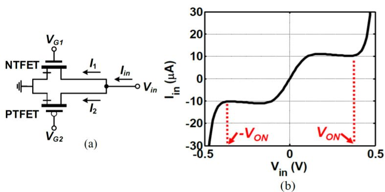
−7
x 10
−7 1
1
x 10 outlier
corner
edge
0.5 core
0.5
(amp)
I(amp)
0 0
C dx
dt
−0.5
Graphene transistor −0.5
PWL approximation
−1
−1 0 1
V (volt) −1
−1 0 1
(a) (b) x (volt)
Fig. 2. (a) Example characteristics of a CNN device for multi-valued
problems; (b) I-V characteristics of the double-layer graphene device at room Fig. 3. DP plots for the representative cases of the four classes with k =
temperature [14], and its Piece-wise linear (PWL) approximation. 7 × 10⁻⁹ and ε = 3 × 10⁻⁹ . The state equilibrium points are marked with
open circles.
Input Final State/Output
where h (xij ) represents the graphene transistor’s I-V charac- Initial State
teristics. In a DP plot, Eq. 3 is plotted as a function of the state 5 5 5
voltage, xij . The shape of the plot can be modulated by the first 10 10 10
15 15 15
two right hand side terms (together called the DP component), 20 20 20
whereas the last three terms’ summation provides an offset to 25 25 25
shift the plot vertically. As such, the equilibrium states of a cell 30
10 20 30
30
10 20 30
30
10 20 30
can be identified at points where the plot intersects the x-axis (a) Single step of graphene transistor based CNN
with a negative slope. Physically it means that at equilibrium,
the current through the capacitor is zero – i.e., the capacitor has Input Initial State Output
completely charged or discharged to the equilibrium voltage. 5 5 5
10 10 10
Below, we use an example problem to further illustrate 15 15 15
quaternary CNN functionality. Given an image of an object 20 20 20
as input (see Fig. 4a), the problem is to identify four distinct 25 25 25
30 30 30
features, e.g., outliers, corners, edges, and cores. Each cell 10 20 30 10 20 30 10 20 30
processes a single pixel of the input image. The input nodes of (b) Step 1 of conventional CNN
the cells are provided with the corresponding input image pixel
Input Initial State Output
(−1 V or +1 V for a white or black pixel, respectively). The
cell states can be initialized with any random values. While a 5 5 5
10 10 10
detailed discussion of template design is beyond the scope of 15 15 15
this paper, the template values are: 20 20 20
25 25 25
0 0 0 −1 −1 −1
" # " #
30 30 30
A = 0 0 0 , B = k −1 8 −1 , Z = −8k + ε 10 20 30 10
(c) Step 2 of conventional CNN
20 30 10 20 30
0 0 0 −1 −1 −1
Input Initial State Output
As the values in the feedback template are equal to zero,
the DP component becomes the negated version of the 5 5 5
device’s I-V. From Fig. 3, we see that each steep-slope current 10
15
10
15
10
15
growth region of the device is responsible for identifying 20 20 20
one particular feature of the problem. For a given feature, 25 25 25
the programmed templates offset the DP component by the 30
10 20 30
30
10 20 30
30
10 20 30
proper amount of current such that the responsible steep-slope (d) Step 3 of conventional CNN
(negated in DP) intersects with the x-axis and results in an
Fig. 4. Simulation results for quaternary classification.
equilibrium state voltage. The ranges of stable voltages for
the features are always finite, and mutually exclusive. Thus,
with proper template design graphene transistor based cells
can reach desired output states. step, Fig. 4a), and the conventional CNN (requires three
computational steps, Fig. 4b-d). The resistor value in the
To verify the cell array dynamics, we augmented a conventional CNN is set to 36 M Ω such that the settling time
MATLAB based simulator [19] that solves a system of for a binary step is similar to that of graphene transistor based
ODEs numerically by using the Runge-Kutta method. For an CNN. During each step, the conventional approach eliminates
M × N CNN array, the system of ODEs consists of M N one particular feature, and passes the remaining features to
equations each defined for a given cell. Each cell in the array the succeeding step. Moreover, step 1 requires pre-processing
requires an initial value for the state voltage which defines the to initialize the state nodes with the input image. Altogether,
initial condition for the cell’s equation. Fig. 4 illustrates the simulation suggest that the conventional CNN takes 59 ns to
simulation results of the quaternary problem solved by both complete the quaternary classification whereas the graphene
the graphene transistor based CNN (in a single computational transistor based CNN needs only 16 ns.Fig. 6. (a) Nonlinear element. (b) Characteristic of the nonlinear element.
The width of the TFETs is 1 µm.
Fig. 5. I-V characteristic of a TFET and a MOSFET. The drain current
is given per width of the transistor. The length of the NMOS is 24 nm, the
minimum in the 22 nm technology.
IV. C IRCUITS FOR M ULTI - VALUED P ROBLEMS
While the previous section illustrates their utility, devices
such as graphene transistors are still in the early stages
of development and additional studies and experiments are
required before these devices can be used in complex systems
such as CNNs. In this section, we show that multi-valued
characteristics can be realized via circuits based on a more
mature beyond-CMOS technology. An InAs TFET technology Fig. 7. (a) Proposed nonlinear element for a ternary cell. (b) Its DC
[20] is considered in this work. The transistors have a channel characteristic when VB1 = VB4 = 0.1V , VB2 = VB3 = −0.1V ,
length of 20 nm, channel thickness of 7 nm and oxide VDD = −VSS = 0.25V and the width of all TFETs is 1 µm.
thickness of 2.5 nm. A verilog-A model is built from T-CAD
device simulations using the method explained in [21]. The
DC characteristic of an N-type TFET is shown in Fig. 5,
where the source terminal of the transistor is grounded and
the drain terminal is changed from -0.5 V to 0.5 V. Compared
to a 22 nm MOSFET [22] [23], TFET shows a higher output
resistance when operating in the saturation region (at a large
positive VDS ), and negative differential resistance (NDR) at
negative drain-source voltages [11].
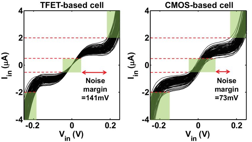
The key component in building a ternary cell is a nonlinear
resistance that can be used to replace the nonlinear term in
Eq. 3. Such a resistance can be created using an NTFET and
PTFET as shown in Fig. 6a. The I-V characteristic of the
resulting element (shown in Fig. 6b) has three low resistance
regions: one low-resistance region around 0 V, where the Fig. 8. (a) Sweeping VB1 and −VB2 from 50 mV to 150 mV, whereas other
two TFETs are in ohmic (linear) region, and two other parameters are similar to those of Fig. 7b. (b) Sweeping VB4 from 50 mV to
low-resistance regions where the p-i-n diode of one of the two 150 mV, while other parameters are similar to those of Fig. 7b.
TFETs is turned on. In between these regions, the resistance
is high (and sometimes negative) because one TFET is in the
saturation, and the other in the NDR region. The I-V curve in characteristic of the cell (shown in Fig. 7b) is similar to that of
Fig. 6b is sufficient for a ternary CNN cell. However, the two Fig. 6b. When Vin is smaller than VB3 − VT H (where VT H is
non-linear regions at the beginning and the end of the curve the threshold voltage of the TFET) such that T3 is turned on, a
are determined by the turn-on voltage of the p-i-n diodes large current will be conducted by the transistor. Similarly for
(VON ) and hence are not programmable. Furthermore, the large positive values of Vin , T4 will conduct a large current.
large value of VON mandates a large peak-to-peak voltage Using the four bias voltages VB1−4 , it is possible to tune the
swing of about 1 V over the nonlinear component. For TFETs characteristic of the element. Fig. 8 illustrates two examples
based on a technology with a bandgap voltage higher than of such tunings. This feature adds to the versatility of a CNN
that of InAs (e.g. a Si-based TFET), VON will be even larger, to handle different applications. Moreover, the small voltage
resulting in a voltage swing and supply voltages well beyond swing of the nonlinear element allows the difference between
the breakdown voltages of other transistors in the cell. the positive and negative supply rails to be as low as 0.5 V.
To add to the programmability of the cell and make it It is instructive to compare the TFET-based nonlinear
compatible with low supply voltages, the nonlinear element element with a CMOS design shown in Fig. 9a. Here, the
in Fig. 7a is proposed. It combines the idea of Fig. 6a with diode-connected transistors T5 and T6 are added to make
a clamp circuit consisting of transistors T3 and T4. For the current passing through T1 and T2 asymmetric. A major
small values of |Vin |, both T3 and T4 are off and the I-V difference between Fig. 7b and Fig. 9b is that in the twoa b c d 80 a b c d
150 60
40
Gradient
100 20
Ty
0
50 −20
−40
0 −60
−80
0 20 40 60 0 20 40 60
T ime T ime
(a) (b)
Fig. 9. (a) CMOS nonlinear element. Note to the increase of transistor length
(L) which is done to improve the output resistance of the MOSFETs. (b) The Fig. 11. (a) Profile of the vertical component of sheer stress, Ty from [15].
I-V characteristic of the CMOS nonlinear element. In region ‘a’, nothing is grasped. Ty increases proportionally with the weight,
in region ‘b’. During ‘c’ the object starts to slip out of the robot’s grasp. In
‘d’, Ty becomes stable as it equal with the kinetic friction force; (b) The
gradient profile of Ty .
Employing the TFET circuit-based ternary CNN, we can
solve the slippage detection problem in 3 steps as shown
in Fig. 12. The input to the system is a 64 × 64 gray scale
image, where each column corresponds to a given sensor, and
the image data reflect the normalized Ty profile over time (as
in Fig. 11a). To account for the 64 sensors in the system, data
for each time step (i.e., a row in the input image) is generated
by a normal distribution with the value from Fig. 11a (for
the given time step) as the mean, and 10% of the value as
Fig. 10. Impact of threshold voltage variations on the characteristic of the
nonlinear elements. variance. The first step calculates the gradient of Ty with
respect to time (similar to the data in Fig. 11b). The output of
the gradient function shows the positive and negative bulges
regions that a high resistance is expected, the resistance of in the gradient profile (i.e., region ‘b’ and ‘c’) as black and
the CMOS-based design is significantly lower than that of the white horizontal strips, respectively.
TFET-based design. This is a consequence of the higher output
resistance of TFETs shown in Fig. 5, and degrades the noise The next step, referred to as thresholding, classifies the
margin when the ternary cell is used in classification tasks. The output data of Step 1 into three distinct classes: positive
robustness of the cells can be evaluated using Monte-Carlo (black) and negative (white) bulges, and no-change (gray)
simulation. Since the mismatch properties of the transistors are (see Fig. 12). The I-V characteristic of the TFET based-
not yet available, the threshold voltage of the transistors was circuit (Fig. 7b) represents a black, white, and gray pixel
varied by adding random errors to the gate voltages. The errors by (0.20, 0.25) V , (−0.25, −0.20) V , and (−0.05, 0.05) V ,
have a Gaussian distribution with a zero mean and a standard respectively. The functionality of this step is explained in
deviation of 10 mV. Fig. 10 shows the result of 100 runs. The Fig. 13a, where the three stable state voltages (marked with
dashed areas show the target input/outputs of the cell assuming open circles) are separated by the two meta-stable points p and
that a given classification task results in cell currents in three q. Any initial state voltage in the ranges of (−∞, p), (p, q),
range of (-∞,2mA), (-0.5mA, 0.5mA), and (2mA,∞). Clearly, and (q, ∞) would eventually settle to one of the three stable
the TFET-based design demonstrates a higher noise margin. voltages that reside in that range. Thus, the output of the
threshold function contains pixels of only three distinct values.
V. C ASE S TUDY The final step is the connected component detection (CCD)
function that projects the presence of a black/white pixel in
As a case study, we consider how CNNs that employ
a horizontal line, to the leftmost column by the same colored
ternary classification circuitry can be used to solve a tactile pixel. As a result, by counting the number of black and white
sensing problem. Initially described in [15], CNNs can be
pixels in the first column, the lengths of region ‘b’ and ‘c’ are
used to process vertical sheer stress – which is an indicator of obtained. The information is processed by the next level for
slippage of an object grasped by a two-fingered robotic hand.
making further decisions. Note that, CCD requires its input
Fig. 11 (from [15]) describes the time-evolution of the vertical pixels to be strictly stratified to one of the class levels for its
sheer stress (denoted as Ty ) and its gradient when an object
correct functionality. This is why the threshold step is required.
starts to slip out of the robotic grasp as a result of increased
weight. Here, the task of the CNN system is to measure the du- As a comparison, a solution of the same problem based
ration of region ‘b’, and ‘c’ locally, which conveys information on a conventional binary CNN requires 5 steps and 2 sets
about how much weight is applied to the object and how fast of hardware (see [15] for more detail). This additional cost
it is slipping. Based on this data, the next level of computation in both hardware and time is due to the fact that a binary
(which may not be located with sensors) can make a decision classifier would only be able to retain information about
about exactly how much grasping force should be applied to one bulge in an image as one of the two stable output
stop the slippage without causing any harm to the object. levels needs to be reserved for representing the empty space.acknowledge Tamás Roska from Pázmány Péter Catholic
University, Hungary for valuable discussion.
R EFERENCES
[1] H. Esmaeilzadeh et al., “Dark silicon and the end of multicore scaling,”
IEEE Micro, vol. 32, no. 3, pp. 122–134, 2012.
[2] L. O. Chua et al., “Cellular Neural Networks: Theory,” IEEE Transac-
tions on Circuits and Systems, vol. 35, no. 10, pp. 1257–1272, 1988.
[3] ——, “Cellular Neural Networks: Applications,” IEEE Transactions on
Circuits and Systems, vol. 35, no. 10, pp. 1273–1290, 1988.
[4] ——, “The CNN paradigm,” IEEE Transactions on Circuits and Sys-
tems I: Fundamental Theory and Applications, vol. 40, no. 3, pp. 147–
156, 1993.
[5] T. Roska et al., “Toward visual microprocessors,” Proceedings of the
IEEE, vol. 90, no. 7, pp. 1244–1257, 2002.
[6] K. Karahaliloglu et al., “Bio-inspired compact cell circuit for reaction-
diffusion systems,” IEEE Transactions on Circuits and Systems II:
Express Briefs, vol. 52, no. 9, pp. 558–562, 2005.
Fig. 12. The Universal Machines on Flows (UMF) [24] description of the [7] J. Kowalski, “0.8 um CMOS implementation of weighted-order statistic
TFET circuit-based CNN for detecting slippage. image filter based on cellular neural network architecture,” IEEE
Transactions on Neural Networks, vol. 14, no. 5, pp. 1366–1374, 2003.
[8] P. Kinget et al., “A programmable analog cellular neural network
−6
x 10 5
CMOS chip for high speed image processing,” IEEE Journal of Solid-
2 a00 =
a00 =
−2
−1 State Circuits, vol. 30, no. 3, pp. 235–243, 1995.
a00 = 0
a00 = 1 [9] M. Hanggi et al., “Cellular neural networks based on resonant tunnelling
1 a00 = 2
diodes,” International Journal of Circuit Theory and Applications,
(amp)
(amp)
vol. 29, no. 5, pp. 487–504, 2001.
0 0 [10] P. Mazumder et al., “Tunneling-Based Cellular Nonlinear Network
p q
C dx
dt
C dx
dt
Architectures for Image Processing,” IEEE Transactions on Very Large
−1 Scale Integration (VLSI) Systems, vol. 17, no. 4, pp. 487–495, 2009.
[11] I. Palit et al., “TFET-based cellular neural network architectures,” in
−2 ISLPED, 2013, pp. 236–241.
−0.2 −0.1 0 0.1 0.2 −5
−2 0 2
x (volt) x (volt) [12] M. Itoh et al., “RTD-based Cellular Neural Networks with Multiple
Steady States,” International Journal of Bifurcation and Chaos, vol. 11,
(a) (b) no. 12, pp. 2913–2959, 2001.
Fig. 13. DP components for (a) TFET circuit-based CNN with the center [13] E. Buccafurri, “Analytical modeling of Silicon based Resonant Tunnel-
matrix element of the feedback template, a00 = 7 × 10⁻⁶ ; (b) Conventional ing Diodes for RF oscillator Application,” Ph.D. dissertation, National
CNN with 1 Ω resistance. Institute of Applied Sciences, Lyon, France, 2010.
[14] L. Britnell et al., “Resonant tunnelling and negative differential con-
ductance in graphene transistors,” Nature Communications, vol. 4, p.
This fact becomes evident also from Fig. 13b, where we 1794, 2013.
can find at most two stable output levels for any of the [15] A. Kis et al., “3D tactile sensor array processed by CNN-UM: a fast
curves. Consequently, the solution of the problem through method for detecting and identifying slippage and twisting motion,”
International Journal of Circuit Theory and Applications, vol. 34, no. 4,
conventional CNN requires two different sets of hardware. pp. 517–531, 2006.
Thus, TFET circuit-based CNN requires fewer computational [16] A. Kanagawa et al., “Cellular neural networks with multiple-valued out-
steps (3 vs. 5), and reduces hardware by half. put and its application,” IEICE Trans. on Fundamentals of Electronics,
vol. E79-A, no. 10, pp. 1658–1663, 1996.
[17] H. Harrer et al., “Discrete-time cellular neural networks,” International
VI. C ONCLUSION Journal of Circuit Theory and Applications, vol. 20, no. 5, pp. 453–467,
1992.
Apart from overcoming the challenges in digital
[18] L. O. Chua et al., Cellular Neural Networks: Foundations and Primer.
computation, emerging devices have a great promise for Cambridge University Press: Cambridge, 2001.
enabling new and enhanced functions for non-von Neumann [19] R. Csaba, MATCNN. Analogic CNN simulation toolbox for MATLAB.
computing paradigms. Moreover, circuits built from emerging Version 1.0. (Research report of the Analogical and Neural Computing
device technologies could also bring clear benefits over Laboratory, DNS-11-1997.). MTA SZTAKI, 1997.
existing approaches. Initial study shows that at the cell level, [20] U. Avci et al., “Comparison of performance, switching energy and
multi-valued classifications improve the energy dissipation by process variations for the TFET and MOSFET in logic,” in Symposium
an order of magnitude. Detail analysis of the energy, power, on VLSI Technology, 2011, pp. 124–125.
and performance – considering other system components (e.g., [21] V. Saripalli et al., “An energy-efficient heterogeneous CMP based on
hybrid TFET-CMOS cores,” in Design Automation Conference (DAC),
the current multipliers) – would be considered in future work. 2011, pp. 729–734.
[22] S. Sinha et al., “Exploring sub-20nm FinFET design with Predictive
ACKNOWLEDGMENT Technology Models,” in Design Automation Conference (DAC), 2012,
pp. 283–288.
This work was supported in part by the Center for Low [23] “PTM-MG model,” [online], June 2012, Available: http://ptm.asu.edu.
Energy Systems Technology (LEAST), one of six centers of [24] T. Roska, “Computational and computer complexity of analogic cellular
STARnet, a Semiconductor Research Corporation program wave computers,” in IEEE International Workshop on Cellular Neural
sponsored by MARCO and DARPA. The authors also Networks and Their Applications, 2002, pp. 323–338.You can also read