Modular design route to construction of designer solution-processed n- and p-type nanoscale hybrid organic-inorganic thermoelectrics
←
→
Page content transcription
If your browser does not render page correctly, please read the page content below
1

Modular design route to construction of designer
solution-processed n- and p-type nanoscale hybrid
organic-inorganic thermoelectrics

Ayaskanta Sahu,1 Boris Russ,1 Norman Su,1,2 Jason D. Forster,1 Preston Zhou,1 Eun Seon
Cho,1 Peter Ercius,3 Nelson E. Coates,4 Rachel A. Segalman,5 and Jeffrey J. Urban1*

1
  The Molecular Foundry, Materials Sciences Division, Lawrence Berkeley National Lab,
Berkeley, CA 94720, USA
2
  Department of Chemical and Biomolecular Engineering, University of California
Berkeley, Berkeley, CA 94720, USA
3
  National Center for Electron Microscopy, Materials Sciences Division, Lawrence
Berkeley National Lab, Berkeley, CA 94720, USA
4
  California Maritime Academy, Vallejo, CA 94720, USA
5
  Departments of Chemical Engineering and Materials, University of California Santa
Barbara, Santa Barbara, CA 93106, USA

*
    email: jjurban@lbl.gov

Abstract
The inability to simultaneously manipulate the thermal and electronic properties of
conventional thermoelectric materials independently has impeded their progress and broad
penetration into terrestrial applications. Hybrid organic/inorganic thermoelectric materials
based on conducting polymers and inorganic nanostructures hold the potential to utilize
both the inherently low thermal conductivity of the polymer and the superior charge
transport properties of the inorganic component. While there are several successful
examples of such materials, there currently exists no general design strategy for generating
hybrid thermoelectric materials. Here, we combine molecular engineering at the
organic/inorganic interface and simple processing techniques to demonstrate a modular
approach enabling de novo design of complex hybrid thermoelectric systems. We
chemically modify the surfaces of inorganic nanostructures and graft conductive polymers
to yield robust solution processable p-type and n-type inorganic/organic hybrid
nanostructures. We tailor the thermoelectric properties of these hybrid materials by varying
the composition of the organic and inorganic components and observe novel non-
monotonic behavior in the electronic properties due to strong chemical interactions
between the components, which leads to peak thermoelectric performance at intermediate
concentrations.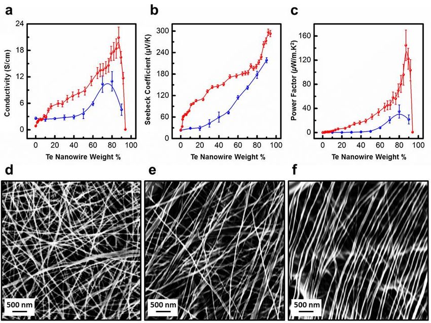
2

Broader Context
Traditional composites of organic and inorganic materials demonstrate additive properties,
which can be modeled by effective medium theories. However, a hybrid material offers
remarkable nonlinear properties that cannot be captured by standard effective medium
principles. While organic/inorganic composites have been extensively used for their
improved mechanical properties, only recently have they been exploited across extremely
diverse fields such as catalysis, coatings, fuel cells, optics, photovoltaics and micro-
electronics. With a plethora of chemical strategies that involve integrative syntheses and
innovative chemical resurfacing at the nanoscale now readily available, one can design
structurally well-defined and complex hybrid nano-architectures with improved and/or
unusual properties. Unfortunately, due to intrinsic chemical and morphological
incongruences between hard and soft components in hybrid thermoelectric materials, it has
proven extremely challenging to exert simultaneous and effective control over both charge
and heat transport. We demonstrate, for the first time, a streamlined synthetic approach that
allows integration of complementary functionalities in a wide-gamut of inorganic-organic
hybrid systems designed specifically for thermoelectric applications. Notably, across
several materials combinations, we observe electronic properties in these hybrid systems
that strongly deviate from those of the individual components – owing to new transport
physics that emerges from strong interactions manifest at the nanoscale interfaces between
the parent constituent materials. These results highlight the importance of controlling and
manipulating the surfaces of hybrid nanostructures as a simple and general but highly
effective strategy to achieve macroscopic control over their thermoelectric transport
properties.

Introduction
Considering the annual increases in world-wide energy demand and thermal management
needs, thermoelectric (TE) devices, which can directly interconvert thermal energy and
electrical energy, and operate without any moving parts and bulk fluids, are promising
technological options for power generation, waste heat recovery, and solid-state cooling.1,
2
  The energy conversion efficiency of a thermoelectric material is quantified by a
dimensionless figure-of-merit, ZT = S2σT/κ, where S is the Seebeck coefficient, σ the
electrical conductivity, κ the thermal conductivity (κ = κe + κl) with κe and κl the electronic
and lattice contributions respectively, and T the absolute temperature (S2σ is typically
termed as the power factor). Due to the inherently competing and conflicting nature of the
parameters (S, σ, κe) contributing to ZT, designing high ZT materials has proven
challenging.3-8 The first renaissance in thermoelectrics emerged when it was realized that
materials with reduced dimensionalities can demonstrate higher figures of merit than their
bulk counterparts due to reductions in κl,, which led to a huge boom in nanostructured
TEs.9-18 However, the deployment of these nanostructured materials has been broadly
impeded by the consumptive synthetic requirements of energy-intensive, high-temperature
processing methods like molecular-beam-epitaxy, metal organic-chemical-vapor-
3

deposition and vapor–liquid solid approaches. Therefore, the economic viability of
implementing a nanomaterial-based TE technology on a large scale using such approaches
remains uncertain.

In this regard, organic materials such as polymers stand out as an attractive proposition for
high performance TEs because of their inherently low thermal conductivities (1-3 orders
of magnitude lower than prototypical inorganics).19 Unfortunately, organics typically
suffer from extremely low power factors and stability issues, which has limited their
implementation as TEs. While evaporated organic thin films demonstrate high
thermopowers, they are limited by poor charge carrier concentrations and/or mobilities.20
In contrast, solution processed polymers21, 22 and all-organic composites23 with high
electrical conductivities are plagued by extremely low thermopowers. Finally, an essential
feature for a functional TE device is the requirement of complementary p- and n-legs,
which is challenging for organic materials, as there exist very few n-type solution-
processed organic materials that are both stable and demonstrate high TE performance.24
Thus, there is an urgent need to discover novel mechanisms and classes of materials to
improve ZT. These trends have spurred research into an entirely new class of TE materials
comprising of a mixture of conductive polymers and inorganic nanostructures.

Hybrid materials are an emerging class of compounds that combine classical inorganic and
organic components, where at least one of the components has dimensions ranging from a
few angstroms to several nanometers, to yield materials that manifest new functionalities
unattainable in traditional composites, which have additive function only. 25 True hybrid
materials exhibit superior performance primarily due to intense non-linear interactions
stemming from electronic or structural changes emerging from the nanoscale interfaces
between its constituent components. Thus, hybrids comprised of inorganic nanostructures
in a matrix of conducting polymer can potentially conjoin the beneficial attributes both of
polymers (e.g. low thermal conductivity, solution processability, flexibility, large area and
roll-to-roll production26) and inorganic nanostructures (e.g. excellent power factors, well-
understood thermoelectric properties, exquisite control over size, shape and composition)
to yield powerful new classes of thermoelectric materials.27 While analogous hybrid
materials have revolutionized the fields of photovoltaics, photodetectors, separation
devices, coatings, fuel cells, catalysts,25, 28 they have been surprisingly scarcely used for
thermoelectric applications, primarily due to the unavailability of robust, high-performance
materials. Principally, this has been due to basic chemical incompatibilities of the hard and
soft components comprising hybrid thermoelectrics; this inevitably leads to electronic and
morphological mismatches which commonly decimates transport. In this article, we
discuss a general strategy to develop solution processed hybrid materials that implements
a synergistic electronic interaction between the inorganic and organic components by re-
engineering their interfacial structure and thus significantly promoting their overall
thermoelectric performance. We demonstrate an unprecedented approach inspired from
“click chemistry”29 to create a myriad of thermoelectric materials comprising of a
conductive polymer and a range of morphologically different inorganic components
spanning from nanodots to nanoplatelets to nanowires. Not only does this strategy allow
us to tap into anisotropic transport regimes but also extract fundamentally novel transport
behavior since quantum confinement effects demonstrated by a zero dimensional
nanocrystalline material can be radically different from a one- and a two-dimensional
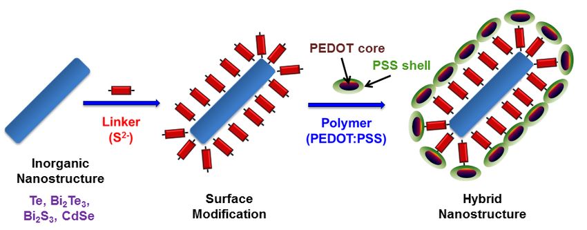
4

semiconductor. Additionally, judicious tuning of the electronic nature of the components
allows us to obtain both n-type and p-type hybrids. Finally, by varying the loading of the
constituents, regardless of the identity of the components, we observe interesting non-
monotonic electronic effects at intermediate loadings suggesting non-effective medium
behavior which manifests from very general physics and hence presents a universal
approach for obtaining high performance electronic materials.

Results and Discussion
While the respective fields of inorganic nanostructures and conductive polymers have
existed for decades, the study of hybrid materials for thermoelectrics is still in its infancy.
The essential criteria for construction of thermoelectric hybrid materials are: 1) chemical
compatibility of both organic and inorganic components, 2) energetic and electronic
matching between both components, and 3) intimate contact spatially between
components. These rigid criteria have, unfortunately, led to limited success stories of
hybrid organic/inorganic materials that can potentially combine the best attributes each of
these materials classes offers.30-35 All hybrid materials possess the potential for property
tuning simply by varying the respective composition of the component materials. However,
more often than not, physical mixtures of hard and soft materials achieved by conventional
blending approaches lead to uncontrolled phase segregation which not only limits the stable
composition range, but also invites substantial sample to sample variation and,
consequently, poor, highly erratic, and irreproducible properties.

One promising strategy is that of in-situ hybrid material construction, which bypasses
traditional problems associated with insulating ligands used for colloidal inorganic
nanostructure synthesis. In one of the first examples of this approach, See et al. proposed
an      in-situ    synthesis   that     generated     tellurium-PEDOT:PSS         (poly(3,4-
ethylenedioxythiophene) polystyrene sulfonate) nanocomposites with extremely
promising thermoelectric properties (ZT=0.1 at 300 K).31 Interestingly, the composite
material demonstrated a conductivity that was significantly higher than either component,
thus characteristic of a hybrid material. This enhancement in conductivity could be
attributed to a highly conductive PEDOT:PSS layer at the interface of the tellurium
nanowires.33, 36, 37 With a huge surface area to volume ratio, most nanostructures are
susceptible to oxidation and/or chemical reactions at the interface. The PEDOT:PSS layer
not only protects the tellurium (Te) nanowire from oxidation but also improves inter-
particle contact so that charges can easily and efficiently flow across the device – a key
requirement for a thermoelectric device.

While the in-situ synthetic scheme provides a general framework for us to develop the next
generation of hybrid organic inorganic materials, it imposes strict restrictions owing to
limited thermal stability of polymers (roughly below 150 °C). Unfortunately, temperatures
required for synthesis of most inorganic nanostructures are typically in the range of 200-
300 °C unlike Te (~90 °C) which severely limits the chemical tunability offered by in-situ
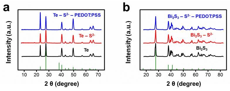
5

syntheses of hybrid nanostructures. Syntheses at lower temperatures often lead to
amorphous nanostructures which severely impairs their charge transport properties. To
alleviate the aforementioned issues, we propose an elegant synthetic approach that
comprises of using the extremely well controlled syntheses of inorganic nanostructures,
replacing the existing ligands (if any) with bi-functional atomic/molecular moieties which
can then couple with the conductive polymer to generate the hybrid. We observe that these
“click chemistry” and/or “coordination chemistry” approaches of using a linker atom or
surface modification to graft conductive polymers onto or even grow the polymer of the
inorganic nanoparticle surface have been extensively used in the fields of photovoltaics38
and optoelectronics.39 To the best of our knowledge, we demonstrate, for the first time, use
of this approach to generate hybrid materials that are amenable for thermoelectric
applications. Choice of the ligand or bridging moiety relies on its ability to prevent
individual nanostructures from aggregation, facilitate dispersion in various solvents and
facilitate linkage to a polymer of choice. In our case, we choose an extremely simple linker
– sulfur atoms - which can potentially bind to any chalcogenide-based nanostructure
system as well as to sulfur atoms in PEDOT (scheme portrayed in Figure 1).

Starting with syntheses of a variety of Te nanowires (with or without ligands),40-42 we
proceed to either replace the original ligands with sulfur ions (S2-) or functionalize the bare
nanostructure surface with these S2- ions (Elemental Analysis with Energy Dispersive
Spectroscopy, Fig. S1, ESI†). Since the sulfur ions attached on the surface of the wires
have a surface charge, they render the Te nanostructures stable in polar solvents, such as
water, and prevent aggregation by electrostatic repulsion between individual nanoparticles
(Zeta potential measurements, Fig. S2, ESI†). This allows us to now blend these S2- capped
Te nanowires with PEDOT:PSS in water. Figure 1a depicts as-synthesized bare Te
nanowires without any capping ligands. Figure 1b shows the same wires with a coating of
PEDOT:PSS. The approach is general and can very well be extended to other
nanostructures as well. To demonstrate the versatility of our technique, we synthesize
hybrid composites comprising of PEDOT:PSS and a host of different inorganic materials
of various shapes and sizes varying from flat two-dimensional Bi2S3 nanoplatelets to one-
dimensional Te nanowires and spherical zero-dimensional CdSe nanocrystals (Figures 1a-
f).

XRD patterns (Figure 2) show that the crystalline structure of the original nanostructure is
preserved both during the surface coating with the linker as well as the coating with
PEDOT:PSS. High resolution TEM images (Fig. S3, ESI†) show that while in-situ low
temperature syntheses of Te-PEDOT:PSS yield polycrystalline samples at times,31 our
approach results in extremely high quality nanostructures. The amount of polymer in the
hybrid can be quantified through thermogravimetric analyses (Fig. S4, ESI†). Depending
on the size of the inorganic nanostructure and the thickness of the polymer coating, the
weight fraction of PEDOT:PSS varies from 15% (nanoplatelets) to as low as 6% (thick
nanowires). Regardless of the quantity of polymer, the resulting hybrids are highly
solution-processable and can be very well dispersed in polar solvents like water (Fig. S5,
ESI†) which renders them highly attractive for cheap roll-to-roll fabrication. Using drop
casting followed by mild annealing (~70 °C) to drive off excess water, we can generate
extremely smooth thin films (Fig. S6, ESI†) which show excellent thermoelectric
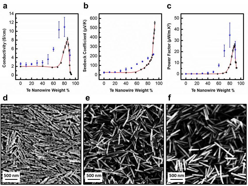
6

properties. In order to compare the performance of our hybrid materials to those generated
by See and Coates et al. (using one-pot syntheses),31, 33 we synthesize Te nanowires with
almost similar diameters and aspect ratios (~ 20) and coat them with PEDOT:PSS. By
combining additional amounts of PEDOT:PSS to the hybrids, we generate a controlled
series of composites with varying organic to inorganic fraction. Figures 3a-c demonstrate
the thermoelectric properties of these films while Figures 3d-f show representative
composite films with different polymer to nanostructure amounts. While there are minor
variations in the absolute values of the Seebeck coefficients and electrical conductivity, we
are able to reproduce the same trends as was observed by Coates et al., in particular the
peak in electrical conductivity which was attributed to a highly conductive layer at the
organic/inorganic interface (i.e. PEDOT:PSS/Te).33 In spite of using an entirely different
scheme to synthesize the hybrid material, we are able to obtain the same result, which
highlights the powerful generality of this hybrid materials approach. Interestingly, we can
now extend our approach to a wholly new material system i.e. bismuth sulfide nanoplatelets
(Fig. S7, ESI†) coated with PEDOT:PSS and remarkably, we observe exactly similar
behavior with a peak in conductivity at intermediate polymer loadings (albeit at a different
concentration as compared to the Te – PEDOT:PSS system) which confirms the
universality of this method. Further, the potency of this method is immediately apparent as
this is the first report of using a polymeric interface to boost the thermoelectric power factor
of bismuth sulfide.

Manipulating aspect ratio of nanostructures provides yet another avenue to control
thermoelectric transport by opening up high electrical conductivity pathways while
impairing thermal conductivity. In-situ techniques used for synthesis of organic-inorganic
hybrids are typically system-specific and offer little control over the aspect ratio of the final
product. Changing the initial polymer to inorganic precursor ratio drastically affects the
nucleation and growth dynamics of the nanostructure; thus proving extremely hard to
manipulate the quality, size and shape of the resulting hybrid. In contrast, our approach
isolates the synthesis of the individual components from their ultimate assembly thus
allowing us to exercise superior control over the morphology of the final structure. In order
to demonstrate the utility of this approach, we synthesize extremely long Te-PEDOT:PSS
nanowires (aspect ratios ~ 1000) having similar diameters to those shown in Figure 3, coat
them with PEDOT:PSS, repeat the casting procedure and the thermoelectric measurements
(Figure 4) and compare both sets of results. We observe a five-fold increase in the
maximum power factor in these long nanowires primarily due to increased electrical
conductivity, which could be attributed due to lower carrier scattering from the
organic/inorganic interface. One could reimagine the hybrid film to be a continuous
network of percolated nanoscale interfaces. A longer nanowire leads to less number of
interfaces over a certain fixed volume thus leading to a higher electrical conductivity.
However, since the electronic properties are dictated by the highly conductive interfacial
polymer layer, having a well-structured and smooth surface in our ex-situ grown NWs
plays a more significant role in the improved thermopower and conductivity values. The
higher quality of the interface between Te and PEDOT:PSS is very well reflected through
time-resolved THz transmission measurements where we observe extremely long
photoconductivity radiative lifetimes (~40x higher values) in our hybrid NWs as compared
to the in-situ grown NWs.37 These results prove that the sulfur functionalization coupled
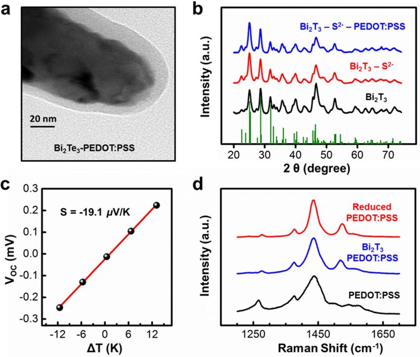
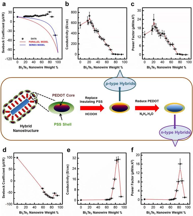
7

with the PEDOT:PSS attachment results in effective passivation of the Te interface with
an extremely low density of surface recombination centers and trap states.

While we have presented only one aspect of the hybrid material by tailoring the length of
the nanowire, our technique presents the potential to not only optimize the size, shape and
identity of the inorganic nanostructure but also the nature of the organic component. We
explore this avenue by doping PEDOT:PSS with formic acid and observe a large increase
in conductivity values (Fig. S8, ESI†) primarily due to the removal of insulating PSS.
However, the Seebeck coefficient decreases at a much faster rate than the increase in
electrical conductivity leading to a maximum power factor value similar to those obtained
in Figure 4 which leads us to believe that there exists a huge scope for optimization to yield
even better performances by manipulating all the above mentioned parameters.

The mechanism behind the peak in conductivity at intermediate polymer loadings was
explained by Coates et al. with a model that invoked interfacial interactions between the
inorganic nanowire and PEDOT:PSS which might lead to conformational changes in the
polymer layer.33 In order to control this phenomenon and enhance its beneficial effects, we
need to gain a fundamental understanding about the interface. We perform X-ray
photoelectron spectroscopy (XPS) studies to gain insight regarding the nature of the
interaction between the inorganic and the organic components– if it is strictly a structural
effect or if there is any chemical bonding/interaction between the species. XPS signals at
S(2p) core edge for PEDOT:PSS (Fig. S9, ESI†) shows two distinct peaks centered around
164.5 eV and 169 eV which can be attributed to signals obtained from PEDOT and PSS
respectively. In contrast, the corresponding spectra for Te-PEDOT:PSS hybrid nanowires
shows a slightly higher fraction (~2%) of PEDOT peak as compared to the PSS peak which
is a signature of de-doping of PEDOT:PSS43 and hence points towards a chemical
interaction between the inorganic and organic components rather than simply a
structural/physical interaction. We presume that this de-doping could be attributed to the
layer of negatively charged sulfur species (linker atoms) on our tellurium nanowires which
can potentially bind to the PEDOT:PSS chains and donate electrons. However, the
magnitude of this effect is tiny and hard to de-convolute since both tellurium and
PEDOT:PSS are p-type materials.

In order to investigate if there indeed exists a charge transfer between the inorganic
nanomaterial and PEDOT:PSS, we proceed to synthesize n-type Bi2Te3 nanowires and coat
them with PEDOT:PSS following the linker method described previously. Figure 5a shows
a representative transmission electron micrograph for the hybrid material and Figure 5b
shows X-ray diffraction patterns that depict the preservation of the crystal structure and
crystallinity of the nanowire before and after polymer incorporation. Interestingly, we
obtain a negative Seebeck coefficient with a modest value of nearly -19.1 µV/K for the
composite (Figure 5c) which, in principle, could simply be attributed to a mixture of an n-
and a p-type material with a mean intermediate Seebeck coefficient. In order to shed more
light on this issue, we perform Raman spectroscopy on thin films of samples of
PEDOT:PSS and Bi2Te3-PEDOT:PSS (Figure 5d). While the Raman spectrum of pristine
PEDOT:PSS shows peaks characteristic of p-doped PEDOT:PSS films,44, 45 the peaks from
the spectrum for the Bi2Te3-PEDOT:PSS film are more intense and well defined. The most
8

intense peak from the pristine film corresponding to Cα=Cβ symmetric stretching is a
combination of neutral (1440 cm−1) and oxidized (1456 cm−1) PEDOT chains.45-47 This
peak is red-shifted in the Bi2Te3-PEDOT:PSS films to 1432 cm−1 and is narrower which
clearly shows the de-doping of PEDOT to neutral states. For comparison, spectrum of de-
doped PEDOT:PSS with hydrazine is also shown.43, 48 Evolution of a new peak at 1521 cm-
1
  and disappearance of the peak at 1260 cm-1 are further indications of the presence of de-
doped PEDOT:PSS thus proving that there is a charge transfer between Bi2Te3 and
PEDOT:PSS and the interaction between the inorganic nanowire and the organic polymer
is undoubtedly of a chemical nature.49

As demonstrated earlier, we can generate a controlled series of Bi2Te3-PEDOT:PSS
composites with varying polymer fractions by adding additional amounts of PEDOT:PSS
to the as-synthesized hybrid. The Seebeck coefficients of the resulting series of materials
are plotted in Figure S10 (ESI†) and show a gradual progress from positive to negative
values with increasing Bi2Te3 fraction (n-type component). These experimentally obtained
values lie between the predicted boundaries as modeled by either series or parallel
connected binary composite thus characteristic of a simple mixture.50 However, the true
hybrid nature of this system is revealed when the composite (PEDOT:PSS portion) is doped
with formic acid.51 The Seebeck coefficients of the resulting series display a non-
monotonic behavior with values consistently higher than PEDOT:PSS over a wide range
of concentrations (Figure 6a). This behavior cannot be captured by either series or parallel
models and thus, cannot be explained by mean field theories. We hypothesize that while
on one hand, Bi2Te3 nanowires reduce the hole concentration in PEDOT:PSS by de-doping,
thus increasing the Seebeck coefficient; the templating of the PEDOT:PSS chains by the
Bi2Te3 nanowires might lead to increased hole mobilities along the interfacial layer. This
interplay between carrier concentrations and mobilities can explain the initial increase in
conductivity (Figure 6b) where the increase in mobility dominates the drop in carrier
concentration. At higher Bi2Te3 concentrations, the carrier concentration is reduced enough
to dominate whatever increased hole mobility might be introduced by the restructuring of
the polymer around the nanowire and thus, we observe a subsequent decrease in
conductivity. The maximum power factor (~24 µW/m.K2) obtained from this system
coincided with the concentration of wires that showed a peak in conductivity (Figures 6b
and 6c). This technique thus presents an amenable way to tune the thermoelectric properties
of heavily doped polymeric materials by controlled de-doping using an inorganic additive.

Ultimately, for a working thermoelectric module, one requires both high-performing and
complementary p-type and n-type materials. Traditionally, it has been extremely hard to
synthesize stable, solution-procesable and efficient n-type organics which has, in turn,
limited the performance and applicability of n-type hybrid material systems. While we
were able to obtain high-performing p-type hybrids using the Te-PEDOT:PSS system, we
wanted to demonstrate the generality and versatility of our approach and extend it to n-type
materials as well. Unfortunately, PEDOT:PSS is a p-type material and even using an n-
type inorganic material like Bi2Te3 did not yield composite materials with high n-type
performance. However, the observation that PEDOT:PSS can potentially be de-doped by
Bi2Te3 through electron transfer motivated us to pursue an approach where if we manage
to invert the nature of the majority charge carrier (from holes to electrons) in PEDOT:PSS
9

and possibly take advantage of the high mobility offered by aligned PEDOT:PSS chains,
we can, in principle, obtain n-type hybrids with promising thermoelectric properties. In
order to remove all holes from PEDOT:PSS, we use an extrinsic de-doping approach
wherein we soak our Bi2Te3-PEDOT:PSS films (synthesized and cast as described earlier)
in various well-known reducing agents used to modulate the optical properties of
PEDOT:PSS such as sodium sulfite, sodium thiosulfate, sodium hydroxide and hydrazine
hydrate.48 The hydrazine hydrate treated samples gave us the best performance in terms of
film quality as well as thermoelectric properties. We used a 2-step process to generate our
films. First, we soaked the as-cast hybrid films in formic acid (or ethylene glycol) to
remove insulating PSS and yield highly ordered and conductive (p-type) Bi2Te3-PEDOT
hybrids (please note that this treatment renders the films insoluble in solvents like water).
Subsequently, these films were dipped in hydrazine monohydrate (~5 volume % in water)
to reduce PEDOT for around 10 minutes and dried at ~80 °C for nearly 20 minutes to
remove any residual solvents. XPS results (Fig. S11, ESI†) demonstrate only one peak at
163.5 eV and clearly show no evidence of peaks corresponding to PSS confirming the
success of the two-step process to effectively de-dope PEDOT:PSS (Fig. S9, ESI†). The
peak at 163.5 eV is also red shifted by nearly 1 eV from what would be expected to be
obtained from PEDOT (164.5 eV). These results hint towards complete removal of
insulating PSS from PEDOT:PSS as well as intense n-type doping of PEDOT. We
performed the treatment for a range of different concentrations of Bi2Te3 and PEDOT:PSS
films and the thermoelectric properties are summarized in Figures 6d-f. Comparing data
from Figures 6a, b and 6d, e for the sample with just PEDOT:PSS, we observe that while
the Seebeck coefficient increases from ~15 µV/K to ~100 µV/K, the electrical conductivity
drops from ~560 S/cm to ~0.2 S/cm which confirms effective reduction. The Seebeck
coefficients for all the analyzed samples were negative within the experimental range (16-
63% by volume and 58-93% by weight of Bi2Te3) thus implying that all our hybrids were
n-type (Figure 6d). As observed in all our previous data, we note a peak in conductivity for
the samples with nearly 80 % (by weight) Bi2Te3 (Figure 6b) which results in a maximum
power factor of ~16 µW/m.K2 which is amongst the highest reported values for an n-type
hybrid material (Figure 6c).

Conclusions
In conclusion, we use a lego-like approach to synthesize both p-type and n-type hybrid
thermoelectrics using a conductive polymer (PEDOT:PSS) and various nanostructured
inorganic materials. We use an interface engineering technique to coat our nanostructures
with a linker molecule that binds to the polymer as well thus generating a robust composite.
Our unique approach leads to intricate control over the organic and inorganic components
and provides synergistic contact at the interface which manifests in extremely promising
thermoelectric properties for the hybrid material. The strategies discussed in this report
could be readily extended to other polymers and organic materials rather than being limited
to PEDOT:PSS and generate novel composites. With the advent of new n-type organic
materials, the methodology could be employed to generate hybrids which are more
conducive towards electron transport as compared to PEDOT:PSS. While we demonstrated
potential applications for thermoelectrics, the possibility to generate both n- and p-type
10

hybrid materials not only holds promise for other electronic applications but also for
exploring fundamental principles like carrier filtering and phonon scattering. The
development of these hybrid materials not only opens up a whole realm of new
opportunities for realizing low cost, flexible and high performance thermoelectrics but also
complements a very fundamental area of science by providing a platform for crucial studies
on interfacial electron and phonon transport dynamics.

Experimental Section
Chemicals and Substrates

Tellurium dioxide (99.9995%), sodium hydroxide (ACS reagent, ≥97.0%, pellets),
potassium hydroxide (≥85% KOH basis, pellets, white), polyvinylpyrrolidone (PVP,
average molecular weight ~ 55,000), ethylene glycol (ReagentPlus®, ≥99%), hydrazine
hydrate (78-82%, iodometric), sodium tellurite (−100 mesh, 99%), bismuth (III) chloride
(99.99%, trace metals basis), oleylamine (technical grade, 70%), sulfur (99.998% trace
metals basis), trioctylphosphine (technical grade, 90%), cadmium oxide (≥99.99% trace
metals basis), hexadecylamine (technical grade, 90%), selenium pellets (99.999%),
ethylene glycol (99.9%), formic acid (reagent grade, ≥95%), bismuth (III) nitrate
pentahydrate (≥99.99% trace metals basis) and methanol (reagent grade, 98%) were
purchased from Sigma Aldrich. Acetone (J.T.Baker®) and isopropyl alcohol (ACS Grade)
were purchased from VWR International. Sodium sulfide (anhydrous, min. 99.5%) were
purchased from Strem Chemicals. N-dodecylphosphonic acid was purchased from PCI
Synthesis. Poly(3,4-ethylenedioxythiophene) polystyrene sulfonate (PEDOT:PSS, Clevios
PH 1000) was purchased from Heraeus Quartz. All chemicals were used as delivered
without further purification. Quartz substrates, 9.5 mm X 9.5 mm, and 0.2 mm thick, were
purchased from Thin Film Devices. -oriented, boron-doped silicon (Si) wafers
(resistivity=0.005–0.01 Ωcm, thickness=525±25 μm) coated with 300 nm of thermal oxide
(SiO2) were purchased from Silicon Valley Microelectronics.

Synthesis of Hybrid Nanostructures

All inorganic nanostructures (bare tellurium nanowires,40 tellurium nanowires with
ligands,41, 42 cadmium selenide nanocrystals,52 bismuth sulfide nanoplatelets,53 bismuth
telluride nanowires32) were synthesized by established literature protocols. For the surface
engineering with S2-, a typical reaction involved adding requisite amounts of Na2S
(typically 4-5 times the number of surface atoms on the nanostructure) in water to a 4-5
mg/ml dispersion of nanosructures in water or hexane in a glass jar with continuous stirring.
Stirring periods varied between 30 minutes to overnight (~16 hours) depending on the
specific system. After the reaction was stopped, the sulfur-capped nanostructures were
centrifuged for ~45 minutes. While the nanostructures crashed out of the dispersion, any
unreacted Na2S and starting ligands (if any) stripped from the nanostructures remained in
the supernatant which was discarded. The precipitated nanostructures were dispersed in
11

water and isolated again with centrifugation. The process was repeated at least 4 times to
ensure the removal of any unbound species and obtain a clean product. Subsequently, an
excess of PEDOT:PSS (typically 2-3 times the number of surface atoms on the
nanostructure) was added to the nanostructures suspended in water and the mixture was
stirred overnight followed by numerous (3-4) rounds of precipitation and re-dispersion
until all unbound PEDOT:PSS was removed from the suspension. Finally, the PEDOT:PSS
capped nanostructures were resuspended in ultrapure 18 MΩ water and stored for further
use.

Sample Characterization

X-ray diffraction (XRD), scanning electron microscopy (SEM), energy dispersive x-ray
spectroscopy (EDS), transmission electron microscopy (TEM), thermo-gravimetric
analysis (TGA), x-ray photoelectron spectroscopy (XPS), and Raman spectroscopy were
used to characterize the size, shape, structure, composition, and optical properties of the
nanostructures. For the XRD, XPS, Raman measurements and SEM imaging, we used
quartz substrates which were sonicated in acetone, isopropanol, and methanol (10 min in
each), rinsed with methanol, dried at 100 °C for nearly 15 minutes and then UV-ozone
treated for 30 minutes. For wide angle XRD, a Bruker-GADDS 8 microdiffractometer was
utilized to collect wide-angle powder patterns (Cu-Kα). Samples were prepared from
concentrated dispersions of nanostructures in solution. Films of these nanostructures were
deposited onto heavily doped Si wafers covered with a thermally grown 300-nm-thick SiO2
layer. For TEM, a Libra120 and an FEI Technai G20 Super Twin Lab6 microscope were
used to image the nanostructures with acceleration voltages of 120 and 200 kV
respectively. Each sample was prepared by depositing a drop of dilute dispersion in
solvents like hexane or methanol onto a 400-mesh carbon-coated copper grid and allowing
the solvent to evaporate at room temperature. SEM images were recorded and EDS
analyses were performed on a Zeiss Gemini Ultra-55 Analytical Scanning Electron
Microscope using beam energy of 5 kV and an In-Lens detector. TGA was acquired using
a Thermal Advantage Q20 calorimeter at a scan rate of 10 °C min-1. An indium standard
was used to calibrate the instrument and nitrogen was used as the purge gas. X-ray
Photoelectron spectra were acquired using PHI 5400 X-ray Photoelectron Spectroscopy
(XPS) System with Al Kα source. The energy resolution was set to 0.1 eV and the
experimental chamber had a base pressure of 1×10⁻⁹ torr. Spectral fitting was performed
using Casa XPS analysis software. Spectral positions were corrected by shifting the
primary C 1s core level position to 284.8 eV, and curves were fit with quasi-Voigt lines
following Shirley background subtraction. Confocal Raman microscopy was performed
using a WITec alpha300 S confocal microscope coupled to a Raman spectrometer (1800
grooves/mm grating) equipped with a CCD detector (UHTS-300). A fiber-coupled laser
operating at 532 nm was used to stimulate Raman scattering. Excitation laser light was
focused into the sample with a Nikon E Plan objective lens with 20× magnification and
NA = 0.4. Light from the sample was collected using the same lens and passed through a
fluorescence filter to remove nonscattered and Rayleigh-scattered laser light and then
focused onto a pinhole at the entrance of an optical fiber that leads to the spectrometer.
Spectra were collected using 30-60 s integration time.

Thermoelectric Measurements
12

Films of nanostructures (typically 5 microns thick) were drop-cast onto a pre-cleaned
quartz substrate (as described above) from a 100 mg/ml dispersion in water and heated at
70 °C for nearly 30 minutes. For conductivity and Seebeck measurements, four 100-nm
thick gold contacts were deposited near the four corners of the drop cast films via thermal
evaporation. Electrical conductivity was measured using a Keithley 2400 Sourcemeter in
4-wire van-der-Pauw configuration. Film thicknesses were estimated by scratching the
nanowire film and measuring the step change with a Veeco Dektak 150 profilometer.
Seebeck coefficient was measured using a homemade setup consisting of two Peltier
devices (Ferrotec) spaced ~4 mm apart. Current was driven through the devices in opposing
polarities, resulting in a temperature gradient about room temperature which varied with
the magnitude of the current. The temperature of the sample was measured using two T-
type thermocouples mounted in micromanipulators. Silicon thermal paste (Wakefield
Thermal S3 Solutions) was utilized between the Peltier devices and the substrate to ensure
good thermal contact. Typically, 5 different temperature gradients (ΔT = +15 °C) were
employed with an equilibration time of 120-180 seconds between temperature changes,
and 10-20 measurements were taken for open circuit voltage (VOC) and averaged using an
Agilent 34401 multimeter. Data for both electrical conductivity and thermopower were
acquired using homemade Labview programs. The value of VOC varied linearly with ΔT
for all of the films within the temperature range measured. Seebeck coefficients were
calculated by a linear fit of VOC vs ΔT.

Acknowledgements
We gratefully acknowledge support through the Department of Energy BES-LBL
Thermoelectrics Program. This work was partially performed at the Molecular Foundry,
Lawrence Berkeley National Laboratory, and was supported by the Office of Science,
Office of Basic Energy Sciences, Scientific User Facilities Division, of the U. S.
Department of Energy under Contract No. DE-AC02-05CH11231. B.R. and N.S gratefully
acknowledge the Department of Defense, AFOSR, for fellowship support under the
National Defense Science and Engineering Graduate Fellowship (DOD-NDSEG). E.S.C.
acknowledges support from the Department of Energy Grant no. DE-FG07ER46426, by
the Bay Area Photovoltaic Consortium (BAPVC), funded under the Sunshot Initiative of
DOE.

Figure Captions
13

Scheme 1: Inorganic nanostructure – PEDOT:PSS hybrids. The surface of the inorganic
material (nanocrystals, nanoplatelets or nanowires) is functionalized with a linker molecule
(S2- in this case) which binds to PEDOT:PSS as well forming a bridge between the
inorganic and organic components resulting in a robust inorganic-organic hybrid material.

Figure 1. Transmission electron microscope (TEM) images showing tellurium nanowires
(a) before and (b) after passivation with PEDOT:PSS. The amorphous layer on the surface
of the nanowire is due to the conformal coating of the polymer. TEM images of (c) Bi2S3
nanoplatelets and (e) CdSe nanocrystals and their corresponding hybrids with PEDOT:PSS
(d, f).

Figure 2. X-ray diffraction patterns for (a) tellurium nanowires and (b) bismuth sulfide
nanoplatelets with as-synthesized nanostructures depicted in black, sulfur-capped
nanostructures depicted in red and hybrid inorganic-PEDOT:PSS nanostructures depicted
in blue. The green bars denote the reference peaks for pure bulk inorganic materials.

Figure 3. Dependence of (a) electrical conductivity, (b) Seebeck coefficient and (c) power
factor on the weight percentage of tellurium (Te) nanowires in the hybrid film with
PEDOT:PSS. The black markers represent the data from this report while the blue markers
depict the data from Coates et al. (Ref. 35) for comparison. The red curve is a guide to the
eye. Vertical error bars represent the variance of measurements over multiple samples.
Horizontal error bars that represent the uncertainty in the weight percentage measurement
are typically in the order of 5% and are not shown in the figure for clarity. Representative
scanning electron microscopy images of hybrid Te nanowire-PEDOT:PSS films with Te
nanowire weight percentages of (d) 92% (e) 82% and (f) 57%.

Figure 4. Dependence of (a) electrical conductivity, (b) Seebeck coefficient and (c) power
factor on the weight percentage of tellurium (Te) nanowires in the hybrid film with
PEDOT:PSS. The red markers represent the data from this report while the blue markers
depict the data from the in-situ synthesis by Coates et al. (Ref. 35) for comparison. The red
and blue curves are guides to the eye. Vertical error bars represent the variance of
measurements over multiple samples. Horizontal error bars that represent the uncertainty
in the weight percentage measurement are typically in the order of 5% and are not shown
in the figure for clarity. Representative scanning electron microscopy images of hybrid Te
nanowire-PEDOT:PSS films with Te nanowire weight percentages of (d) 94% (e) 87% and
(f) 70%.
14

Figure 5. (a) Transmission electron microscope (TEM) image showing a hybrid bismuth
telluride-PEDOT:PSS nanowire. The amorphous layer on the surface of the nanowire is
due to the conformal coating of the polymer. (b) X-ray diffraction patterns for bismuth
telluride (Bi2Te3) nanowires with as-synthesized bare nanowires depicted in black, sulfur-
capped nanowires depicted in red and hybrid Bi2Te3-PEDOT:PSS nanowires depicted in
blue. The green bars denote the reference peaks for bulk Bi2Te3. (c) Open circuit voltage
(VOC) versus applied temperature gradient (ΔT) for films of Bi2Te3-PEDOT:PSS
nanowires. The Seebeck coefficient is derived from the slope of the linear fit (R2 value of
0.9998). Error bars representing the standard deviation from averaging 10 readings for each
temperature gradient are captured within the data marker. (d) Raman spectra of thin films
cast from pure PEDOT:PSS, Bi2Te3-PEDOT:PSS nanowires and PEDOT:PSS treated
(reduced) with hydrazine hydrate on glass substrates. The spectra obtained from Bi2Te3-
PEDOT:PSS nanowires matches that of reduced PEDOT:PSS indicating charge (electron)
transfer from Bi2Te3 into PEDOT:PSS.

Figure 6. Scheme to obtain both p- and n-type Bi2Te3 hybrid nanostructures. Films of as-
synthesized Bi2Te3-PEDOT:PSS nanowires are treated with formic acid to remove
insulating PSS and generate high conductivity p-type hybrids (a-c) while those treated with
formic acid followed by hydrazine hydrate result in n-type hybrids (d-f). Dependence of
(a, d) Seebeck coefficient, (b, e) conductivity and (c, f) power factor on the weight
percentage of bismuth telluride (Bi2Te3) nanowires in the p-type and n-type hybrid films
respectively. Horizontal error bars represent the uncertainty in the weight percentage
measurement. Vertical error bars represent the variance of measurements over multiple
samples. For the Seebeck measurements, the vertical error bars are captured within the data
marker. The blue and red curves for the Seebeck coefficient data in (a) are from a series-
connected and a parallel-connected two-component model respectively. The red curves for
the data in (b-f) serve as a guide to the eye.
15

Scheme 1

Figure 1
16

     Figure 2

     Figure 3
17 Figure 4
18

     Figure 5
19 Figure 6
20

References

1.    L. E. Bell, Science, 2008, 321, 1457-1461.
2.    G. J. Snyder and E. S. Toberer, Nature Materials, 2008, 7, 105-114.
3.    T. M. Tritt and M. A. Subramanian, MRS Bulletin, 2006, 31, 188-194.
4.    G. A. Slack and M. A. Hussain, Journal of Applied Physics, 1991, 70, 2694-
      2718.
5.    G. A. Slack, in CRC Handbook of Thermoelectrics, CRC Press, 1995.
6.    D. M. Rowe, CRC Handbook of Thermoelectrics, CRC Press, Boca Raton,
      FL, 1995.
7.    D. M. Rowe, Journal of Physics F-Metal Physics, 1974, 7, 1843-1846.
8.    G. D. Mahan and J. O. Sofo, Proceedings of the National Academy of
      Sciences of the United States of America, 1996, 93, 7436-7439.
9.    L. D. Hicks and M. S. Dresselhaus, Physical Review B, 1993, 47, 16631-
      16634.
10.   R. Venkatasubramanian, E. Siivola, T. Colpitts and B. O'Quinn, Nature,
      2001, 413, 597-602.
11.   T. C. Harman, P. J. Taylor, M. P. Walsh and B. E. LaForge, Science, 2002,
      297, 2229-2232.
12.   A. I. Hochbaum, R. Chen, R. D. Delgado, W. Liang, E. C. Garnett, M.
      Najarian, A. Majumdar and P. Yang, Nature, 2008, 451, 163-167.
13.   B. Poudel, Q. Hao, Y. Ma, Y. Lan, A. Minnich, B. Yu, X. Yan, D. Wang, A.
      Muto, D. Vashaee, X. Chen, J. Liu, M. S. Dresselhaus, G. Chen and Z. Ren,
      Science, 2008, 320, 634-638.
14.   J. P. Heremans, V. Jovovic, E. S. Toberer, A. Saramat, K. Kurosaki, A.
      Charoenphakdee, S. Yamanaka and G. J. Snyder, Science, 2008, 321, 554-
      557.
15.   A. I. Boukai, Y. Bunimovich, J. Tahir-Kheli, J.-K. Yu, W. A. Goddard, III and
      J. R. Heath, Nature, 2008, 451, 168-171.
16.   W. Kim, J. Zide, A. Gossard, D. Klenov, S. Stemmer, A. Shakouri and A.
      Majumdar, Physical Review Letters, 2006, 96, 045901.
17.   C. J. Vineis, A. Shakouri, A. Majumdar and M. G. Kanatzidis, Advanced
      Materials, 2010, 22, 3970-3980.
18.   M. S. Dresselhaus, G. Chen, M. Y. Tang, R. G. Yang, H. Lee, D. Z. Wang,
      Z. F. Ren, J. P. Fleurial and P. Gogna, Advanced Materials, 2007, 19, 1043-
      1053.
19.   Z. Han and A. Fina, Progress in Polymer Science, 2011, 36, 914-944.
20.   K. Harada, M. Sumino, C. Adachi, S. Tanaka and K. Miyazaki, Applied
      Physics Letters, 2010, 96, 253304.
21.   O. Bubnova, Z. U. Khan, A. Malti, S. Braun, M. Fahlman, M. Berggren and
      X. Crispin, Nature Materials, 2011, 10, 429-433.
22.   G. H. Kim, L. Shao, K. Zhang and K. P. Pipe, Nature Materials, 2013, 12,
      719-723.
21
23. C.-K. Mai, B. Russ, S. L. Fronk, N. Hu, M. B. Chan-Park, J. J. Urban, R. A.
Segalman, M. L. Chabinyc and G. C. Bazan, Energy & Environmental
Science, 2015, 8, 2341-2346.
24. B. Russ, M. J. Robb, F. G. Brunetti, P. L. Miller, E. E. Perry, S. N. Patel, V.
Ho, W. B. Chang, J. J. Urban, M. L. Chabinyc, C. J. Hawker and R. A.
Segalman, Advanced Materials, 2014, 26, 3473-3477.
25. E. S. Cho, N. E. Coates, J. D. Forster, A. M. Ruminski, B. Russ, A. Sahu,
N. C. Su, F. Yang and J. J. Urban, Advanced Materials, 2015, 27, 5744-
5752.
26. A. Facchetti, Chemistry of Materials, 2011, 23, 733-758.
27. D. V. Talapin, J.-S. Lee, M. V. Kovalenko and E. V. Shevchenko, Chemical
Reviews, 2010, 110, 389-458.
28. C. Sanchez, P. Belleville, M. Popall and L. Nicole, Chem. Soc. Rev., 2011,
40, 696-753.
29. H. C. Kolb, M. G. Finn and K. B. Sharpless, Angewandte Chemie
International Edition, 2001, 40, 2004-2021.
30. B. Zhang, J. Sun, H. E. Katz, F. Fang and R. L. Opila, ACS Applied Materials
& Interfaces, 2010, 2, 3170-3178.
31. K. C. See, J. P. Feser, C. E. Chen, A. Majumdar, J. J. Urban and R. A.
Segalman, Nano Letters, 2010, 10, 4664-4667.
32. M. He, J. Ge, Z. Lin, X. Feng, X. Wang, H. Lu, Y. Yang and F. Qiu, Energy
& Environmental Science, 2012, 5, 8351-8358.
33. N. E. Coates, S. K. Yee, B. McCulloch, K. C. See, A. Majumdar, R. A.
Segalman and J. J. Urban, Advanced Materials, 2013, 25, 1629-1633.
34. S. K. Yee, N. E. Coates, A. Majumdar, J. J. Urban and R. A. Segalman,
Physical Chemistry Chemical Physics, 2013, 15, 4024-4032.
35. Y. Du, K. F. Cai, S. Chen, P. Cizek and T. Lin, ACS Applied Materials &
Interfaces, 2014, 6, 5735-5743.
36. J. N. Heyman, B. A. Alebachew, Z. S. Kaminski, M. D. Nguyen, N. E. Coates
and J. J. Urban, Applied Physics Letters, 2014, 104, 141912.
37. J. N. Heyman, A. Sahu, N. E. Coates, B. Ehmann and J. J. Urban, MRS
Online Proceedings Library, 2015, 1742.
38. B. R. Saunders and M. L. Turner, Advances in Colloid and Interface
Science, 2008, 138, 1-23.
39. E. Holder, N. Tessler and A. L. Rogach, Journal of Materials Chemistry,
2008, 18, 1064-1078.
40. B. Mayers, B. Gates, Y. Yin and Y. Xia, Advanced Materials, 2001, 13,
1380-1384.
41. G. Q. Zhang, H. Y. Fang, H. R. Yang, L. A. Jauregui, Y. P. Chen and Y. Wu,
Nano Letters, 2012, 12, 3627-3633.
42. G. Q. Zhang, B. Kirk, L. A. Jauregui, H. R. Yang, X. F. Xu, Y. P. Chen and
Y. Wu, Nano Letters, 2011, 12, 56-60.
43. S. H. Lee, H. Park, S. Kim, W. Son, I. W. Cheong and J. H. Kim, Journal of
Materials Chemistry A, 2014, 2, 7288-7294.
44. J. Ouyang, Q. Xu, C.-W. Chu, Y. Yang, G. Li and J. Shinar, Polymer, 2004,
45, 8443-8450.22
45. S. Garreau, G. Louarn, J. P. Buisson, G. Froyer and S. Lefrant,
Macromolecules, 1999, 32, 6807-6812.
46. W. W. Chiu, J. Travas-Sejdic, R. P. Cooney and G. A. Bowmaker, Synth.
Met., 2005, 155, 80-88.
47. W. W. Chiu, J. Travas-Sejdic, R. P. Cooney and G. A. Bowmaker, J. Raman
Spectrosc., 2006, 37, 1354-1361.
48. N. Massonnet, A. Carella, O. Jaudouin, P. Rannou, G. Laval, C. Celle and
J.-P. Simonato, Journal of Materials Chemistry C, 2014, 2, 1278-1283.
49. I. Cruz-Cruz, M. Reyes-Reyes, I. A. Rosales-Gallegos, A. Y. Gorbatchev, J.
M. Flores-Camacho and R. López-Sandoval, The Journal of Physical
Chemistry C, 2015, 119, 19305-19311.
50. Y. Gelbstein, Journal of Applied Physics, 2009, 105, 023713.
51. D. A. Mengistie, M. A. Ibrahem, P.-C. Wang and C.-W. Chu, ACS Applied
Materials & Interfaces, 2014, 6, 2292-2299.
52. P. Reiss, J. Bleuse and A. Pron, Nano Letters, 2002, 2, 781-784.
53. R. Malakooti, L. Cademartiri, Y. Akcakir, S. Petrov, A. Migliori and G. A.
Ozin, Advanced Materials, 2006, 18, 2189-2194.You can also read