ON-SUBSTRATE JOULE EFFECT HEATING BY PRINTED MICRO-HEATER FOR THE PREPARATION OF ZNO SEMICONDUCTOR THIN FILM - MDPI
←
→
Page content transcription
If your browser does not render page correctly, please read the page content below
micromachines

Article
On-Substrate Joule Effect Heating by Printed
Micro-Heater for the Preparation of ZnO
Semiconductor Thin Film
Van-Thai Tran 1 , Yuefan Wei 2             and Hejun Du 1, *
 1   School of Mechanical and Aerospace Engineering, Nanyang Technological University, 50 Nanyang Avenue,
     Singapore 639798, Singapore; vanthai.tran@ntu.edu.sg
 2   Advanced Remanufacturing and Technology Centre, 3 Cleantech Loop, Singapore 637143, Singapore;
     wei_yuefan@artc.a-star.edu.sg
 *   Correspondence: MHDU@ntu.edu.sg; Tel.: +65-6790-4783

 Received: 13 April 2020; Accepted: 9 May 2020; Published: 10 May 2020

 Abstract: Fabrication of printed electronic devices along with other parts such as supporting structures
 is a major problem in modern additive fabrication. Solution-based inkjet printing of metal oxide
 semiconductor usually requires a heat treatment step to facilitate the formation of target material.
 The employment of external furnace introduces additional complexity in the fabrication scheme,
 which is supposed to be simplified by the additive manufacturing process. This work presents the
 fabrication and utilization of micro-heater on the same thermal resistive substrate with the printed
 precursor pattern to facilitate the formation of zinc oxide (ZnO) semiconductor. The ultraviolet (UV)
 photodetector fabricated by the proposed scheme was successfully demonstrated. The performance
 characterization of the printed devices shows that increasing input heating power can effectively
 improve the electrical properties owing to a better formation of ZnO. The proposed approach using
 the on-substrate heating element could be useful for the additive manufacturing of functional material
 by eliminating the necessity of external heating equipment, and it allows in-situ annealing for the
 printed semiconductor. Hence, the integration of the printed electronic device with printing processes
 of other materials could be made possible.

 Keywords: inkjet printing; zinc oxide; heat treatment; micro-heater; semiconductor

1. Introduction
     Exploration of inkjet printing for the fabrication of electronic devices has recently become a trendy
research topic due to the remarkable advantages of the digital-additive fabrication such as saving
material and time, high resolution, and compatibility with different materials [1,2]. These advantages of
inkjet printing have been widely employed for the fabrication of semiconductor devices [3,4]. Thanks to
its outstanding features and abundance, zinc oxide (ZnO) has attracted considerable attention and
effort in the additive fabrication of electronics devices such as solar cells [5,6], photodetectors [3,7],
and transistors [8,9]. Additive manufacturing of inorganic material from a precursor compound
usually requires a heat treatment step in order to convert precursors to the required material [10,11].
However, the annealing process using an external furnace might restrain the progress of 3D printed
integrative devices because of the added complexity of the fabrication system.
     Low temperature processing of metal oxide has been intensively studied via different approaches,
such as ultraviolet (UV) annealing [12,13] and laser sintering [14], in order to facilitate the formation of
metal oxide by heating effect of high energy light beam, which requires high complexity setup for the
processing system. Furthermore, direct use of nanoparticle ink was considered instead of precursor
ink [15]. However, added surfactant to keep nanoparticle ink stable might be an issue for electronic

Micromachines 2020, 11, 490; doi:10.3390/mi11050490                      www.mdpi.com/journal/micromachines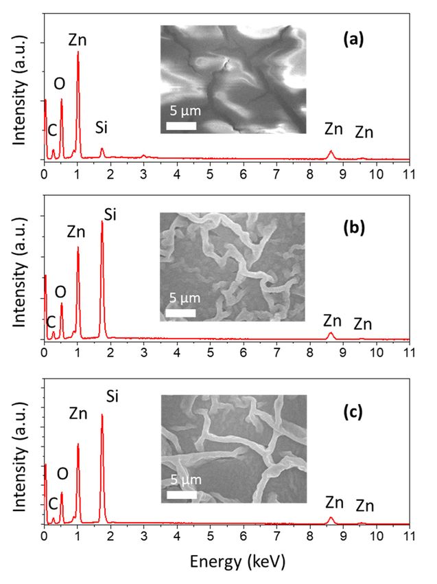
Micromachines 2020, 11, 490                                                                        2 of 11

application because it might change the properties of printed material. Alternatively, using local
Joule heating to form metal oxide by thermal decomposition of precursor compound is an interesting
approach to prepare small-size metal oxide pattern [16].
      Joule heating is the phenomenon in which heat is generated from a conductive material when
there is an electrical current run through the conductor. The power consumed is proportional to the
square of the electrical current and the resistance of the conductor [17]. A micro-heater working on the
Joule heating principle possesses advantages such as local heat and optimized energy consumption.
Therefore, the resistive heater has been employed in application that requires localized heating
and temperature control at small scale, such as activation of gas sensing device [18,19], moisture
monitoring [20], and local growth of semiconductor nanostructures [21]. The traditional approach of
preparing conductive patterns is using photolithography to deposit and remove certain parts of the
conductive film and forming the required shape of the film. As this method has its own drawbacks,
such as the high complexity and time-consuming, additive manufacturing could be a promising
candidate for fabrication of micro-heaters [22].
      In this work, a facile and versatile fabrication process for additive fabrication of semiconductor
using inkjet printing and on-substrate heating was proposed. The printed conductive material is
further employed for another role, which is the heating element for later processes. Zinc precursor ink
is then printed on the same substrate. Eventually, electrical power was applied to the micro-heater to
generate heat, which facilitates the decomposition of the zinc salt and the formation of ZnO. Therefore,
the necessity for an external bulky furnace is eliminated. The generation of ZnO was examined by the
elemental survey of zinc (Zn) and oxygen (O) component in energy-dispersive X-ray spectroscopy (EDS)
and the aid of thermogravimetric analysis (TGA). In order to demonstrate the obtained semiconductor
film, a UV photodetector application was prepared and characterized. The influence of electrical power
during Joule heating to photodetector performance is also evaluated.

2. Materials and Methods
     A commercialized Dimatix 2831 inkjet printer (Fujifilm Dimatix, Inc, Santa Clara, CA, USA)
was employed in all printing steps described in this work using 10 pL cartridge with 16 nozzles.
The silicon/silicon dioxide (Si/SiO2 ) substrate (Bonda Technology Pte Ltd, Singapore) was cleaned
before the printing of silver ink to construct the electrodes and heater. The substrate was cleaned in
acetone and rinsed with isopropanol, then it was dried out by a manual air blower.
     A commercial silver nanoparticle ink (silver dispersion 736465, Sigma-Aldrich, St. Louis, MO,
USA) was employed for the printing of the silver patterns. Detail of the printing step has been
discussed in our previous report [23]. The waveform applied to piezoelectric nozzle to jet ink is shown
in Figure A1a (Appendix A). Peak firing voltage was set at 19 V. Drop-spacing was set at 40 µm to
ensure the continuity of the printed silver line. Single layer was selected for printing of electrodes
and four-layers was selected for printing of micro-heater. Cartridge temperature was set at 35 ◦ C,
however, due to the printer platen temperature was set at 60 ◦ C and the close distance of the cartridge
and the substrate during printing, the cartridge temperature may rise to about 40 ◦ C during printing.
The printed pattern was left on the platen of the printer for 10 min for solvent vaporization.
     Printed single line of conductive silver features 100 µm in width, and the thickness is about 200 nm
as reported in our previous works [23]. The as-printed single line resistance was measured as 15.5 Ω.
Due to the Joule heating process using 4-W power, the resistance was reduced to 5.0 Ω as the effect
of sintering.
     Figure 1 depicts the fabrication of the device using Joule heating. Printed metal patterns, serving
as electrical contacts for the sensor as well as the micro-heater, was printed on the first step of the
fabrication process (Figure 1a). The micro-heater composes of two contacting pad and a single line of
conductive silver serving as a heating resistor. Then, direct current was applied to the micro-heater,
which consumes 4-W power and converts it to heat energy for 5 min (Figure 1b). The generated heat
promotes the sintering of silver electrodes and improves the bonding to substrate. The power applied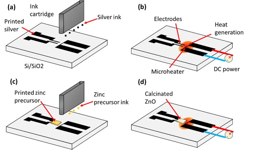
Micromachines 2020, 11, 490                                                                                  3 of 11
Micromachines 2020, 11, 490                                                                                   3 of 11

 source
to      when monitoring
   the micro-heater        the current.
                    was manually         During
                                    adjusted    the Joulethe
                                             by turning    heat  treatment,
                                                             voltage  of thethe  resistance
                                                                             direct  current of thepower
                                                                                             (DC)   micro-
source when monitoring the current. During the Joule heat treatment, the resistance of the micro-heatera
 heater changed  due to sintering effect which require a careful  adjustment  of  voltage. For  example,
 5 W ofdue
changed    power   was obtained
             to sintering          by require
                          effect which  turninga careful
                                                 the voltage    to 5.0of V
                                                         adjustment         while For
                                                                         voltage.   theexample,
                                                                                         current areached
                                                                                                   5 W of
 1.0 A.
power was obtained by turning the voltage to 5.0 V while the current reached 1.0 A.

     Figure 1. Fabrication step of the sensor using including printed micro-heater. (a) Printing of conductive
      Figure 1. Fabrication step of the sensor using including printed micro-heater. (a) Printing of
     pattern for the metal contacts and heater. (b) Applying direct current (DC) power to the micro-heater to
      conductive pattern for the metal contacts and heater. (b) Applying direct current (DC) power to the
     generate heat and sinter silver. (c) Deposition of zinc salt ink over the printed electrodes. (d) Applying
      micro-heater to generate heat and sinter silver. (c) Deposition of zinc salt ink over the printed
     DC power again to the micro-heater to calcinate ZnO.
      electrodes. (d) Applying DC power again to the micro-heater to calcinate ZnO.
     A 50 mM zinc precursor solution was formulated by dissolving of zinc acetate dihydrate
      A 50 mM zinc precursor solution was formulated by dissolving of zinc acetate dihydrate
(Zn(CH3 COO)2 ·2H2 O) to ethanol. Another cartridge was used to print the zinc precursor after the
 (Zn(CH3COO)2·2H2O) to ethanol. Another cartridge was used to print the zinc precursor after the
replacement of the silver ink cartridge by zinc precursor ink cartridge. A rectangular pattern of the
 replacement of the silver ink cartridge by zinc precursor ink cartridge. A rectangular pattern of the
zinc salt solution is printed over the metal contacts, which is nearby the micro-heater (Figure 1c).
 zinc salt solution is printed over the metal contacts, which is nearby the micro-heater (Figure 1c). The
The beneath substrate was kept heated at a temperature of 60 ◦ C during printing to facilitate the
 beneath substrate was kept heated at a temperature of 60 °C during printing to facilitate the
evaporation of the solvent and reduce the spreading of solution over the surface.
 evaporation of the solvent and reduce the spreading of solution over the surface.
     Ten layers of zinc precursor was printed with a designed pattern of 60 pixels by 50 pixels.
      Ten layers of zinc precursor was printed with a designed pattern of 60 pixels by 50 pixels. Zinc
Zinc precursor ink printing parameters were optimized to ensure the stability during printing.
 precursor ink printing parameters were optimized to ensure the stability during printing. The
The waveform was given in Figure A1b (Appendix A) with peak voltage at 19 V. The cartridge was
 waveform was given in Figure A1b (Appendix A) with peak voltage at 19 V. The cartridge was kept
kept at room temperature. Drop spacing, defining by the distance of two nearby droplets, was set at
 at room temperature. Drop spacing, defining by the distance of two nearby droplets, was set at
10 µm, so that it is necessary to calibrate the cartridge holder angle during printing different materials.
 10 μm, so that it is necessary to calibrate the cartridge holder angle during printing different
     After the printing of the precursor, electrical current was applied to the resistive heater again
 materials.
for 5 min (Figure 1d). Two sets of samples which have 4-W and 5-W applied power were studied
      After the printing of the precursor, electrical current was applied to the resistive heater again for
along with the samples without the treatment. A thermal camera (NEC F30W, AVIO, Turin, Italy) was
 5 min (Figure 1d). Two sets of samples which have 4-W and 5-W applied power were studied along
employed to measure the temperature of the device during the Joule heating process.
 with the samples without the treatment. A thermal camera (NEC F30W, AVIO, Turin, Italy) was
     Thermogravimetric analysis (TGA) using the equipment TGA Q500 (TA Instruments, New Castle,
 employed to measure the temperature of the device during the Joule heating process.
DE, USA) was utilized for studying the formation of zinc oxide by thermal process. The heating rate
      Thermogravimetric analysis (TGA) using the equipment TGA Q500 (TA Instruments, New
we used for TGA is 10 ◦ C/min. Film morphology and elemental study were characterized by field
 Castle, DE, USA) was utilized for studying the formation of zinc oxide by thermal process. The
emission–scanning electron microscope (FE–SEM, JOEL 7600F, JEOL Ltd., Tokyo, Japan) and energy
 heating rate we used for TGA is 10 °C/min. Film morphology and elemental study were characterized
dispersive X-ray spectroscopy (EDS) (Oxford Instruments, Abingdon, UK). In order to characterize the
 by field emission–scanning electron microscope (FE–SEM, JOEL 7600F, JEOL Ltd., Tokyo, Japan) and
performance of the Joule heating processed sensor, an ultraviolet light-emitting diode which emits
 energy dispersive X-ray spectroscopy (EDS) (Oxford Instruments, Abingdon, United Kingdom). In
365 nm wavelength was used to illuminate the sensor and measure the photocurrent under dark or
 order to characterize the performance of the Joule heating processed sensor, an ultraviolet light-
lighting condition. The photocurrent was recorded using a source metering unit (SMU B2902A, Agilent,
 emitting diode which emits 365 nm wavelength was used to illuminate the sensor and measure the
Santa Clara, CA, USA).
 photocurrent under dark or lighting condition. The photocurrent was recorded using a source
 metering unit (SMU B2902A, Agilent, Santa Clara, CA, USA).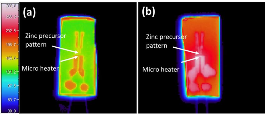
Micromachines 2020, 11, 490 4 of 11
Micromachines 2020, 11, 490 4 of 11
3. Results
3. Results
3.1. Sintering of Printed Silver
3.1. Sintering of Printed Silver
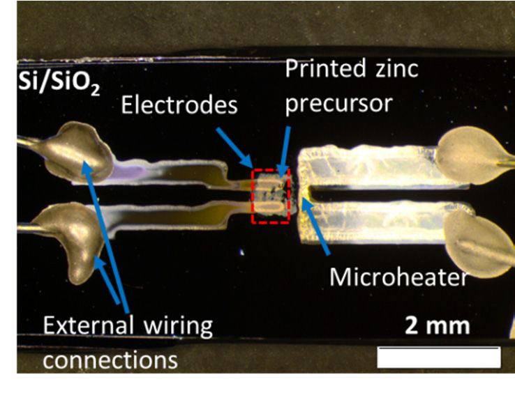
The structure of the device is depicted in Figure 2, which shows three main components of the
The deposited
devices structure ofonthe devicesubstrate.
Si/SiO is depicted in Figure
While 2, which electrodes
the common shows three andmain
the components
micro-heaterofwere
the
2
devices deposited on Si/SiO 2 substrate. While the common electrodes and the micro-heater were
printed on the first layer, the zinc precursor was printed at last. The zinc precursor appears as a white
printed on the first layer, the zinc precursor was printed at last. The zinc precursor appears as a white
rectangle pattern over the silver electrodes. Thus, the photodetector utilizes the metal-semiconductor
rectangle pattern
contacts with theover the silver electrodes.
two-terminals Thus,low-magnification
structure. Two the photodetectorFE–SEM
utilizes the metal-semiconductor
images of samples before
contacts
and after heat treatment was presented in Figure A2 (Appendix A) to provide a bettersamples
with the two-terminals structure. Two low-magnification FE–SEM images of before
understanding
and after
of the heatoftreatment
effect was presented
heat treatment in Figure A2 (Appendix A) to provide a better understanding
to the film.
of the effect of heat treatment to the film.
Figure 2. Optical image of the printed Joule heating device showing the three main components of the
Figure 2. Optical image of the printed Joule heating device showing the three main components of
device, such as electrodes section, printed zinc salt film, and micro-heater. The picture was taken after
the device, such as electrodes section, printed zinc salt film, and micro-heater. The picture was taken
the heat treatment of the ZnO pattern.
after the heat treatment of the ZnO pattern.
The effect of Joule heating on the nanostructure of printed silver could be observed in Figure 3,
which The effectthe
shows of sintering
Joule heating on the
of silver nanostructure
nanoparticles. of printed
Printed silversilver could be observed
film composes in Figure
of separated 3,
particles
which shows
after the the sintering
evaporation of theof silver nanoparticles.
solvent. Printed
The sintering effect silver film composes
is significantly depending ofon
separated particles
the distance from
after
the heater. At the electrode section (Figure 3b), which is distinct from the radiation source, thedistance
the evaporation of the solvent. The sintering effect is significantly depending on the particle
from theapproximately
size of heater. At the 80electrode
to 100 nmsection
could(Figure 3b), which
be observed, is distinct
which from thefrom
is an increase radiation source,
the size the
of about
particle
50 nm ofsize
theofunsintered
approximately 80 to
particles 100 nm
(Figure could be observed, which is an increase from the size of
3a).
about 50 nm of the unsintered particles (Figure 3a).
3. Field
Figure 3.
Figure Field emission–scanning
emission–scanningelectron microscope
electron microscope(FE–SEM)
(FE–SEM)images showshow
images the sintering of printed
the sintering of
silver nanoparticles ink by the resistive heating. (a) The printed silver nanoparticles without annealing.
printed silver nanoparticles ink by the resistive heating. (a) The printed silver nanoparticles without
(b) The silver
annealing. (b) nanoparticles at electrodeatsection
The silver nanoparticles after
electrode annealing.
section after annealing.
Heating radiation from resistive effect is the main source that induces the sintering of the printed
Heating radiation from resistive effect is the main source that induces the sintering of the printed
silver pattern. In Figure 4a, the heater witnesses a notable change of film morphology, such as particle
silver pattern. In Figure 4a, the heater witnesses a notable change of film morphology, such as particle
agglomeration up to the size of 200 nm. As the previous discussion has pointed out, the remote
agglomeration up to the size of 200 nm. As the previous discussion has pointed out, the remote
pattern exhibits minor sintering effect, while at the center of heat source, major agglomeration could be
pattern exhibits minor sintering effect, while at the center of heat source, major agglomeration could
observed. Later analysis of temperature distribution shows that this is indeed a result of gradually
be observed. Later analysis of temperature distribution shows that this is indeed a result of gradually
reduce of temperature in the substrate. Although the sintering of silver could improve the electrical
properties of the conductive pattern, a severe agglomeration of silver nanoparticles could lead to the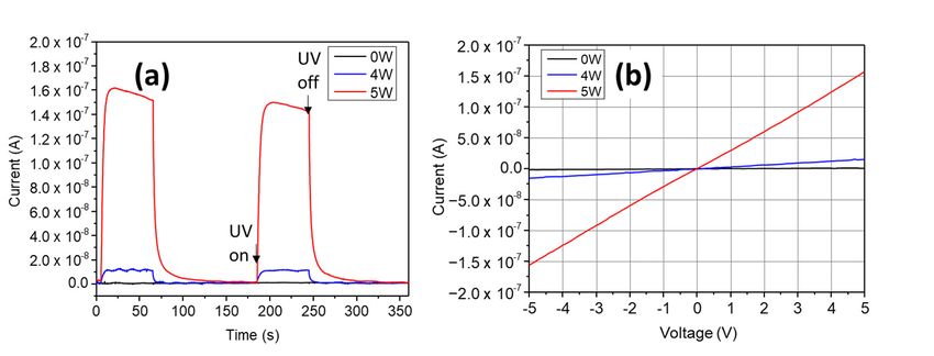
Micromachines 2020, 11, 490 5 of 11
reduce of temperature in the substrate. Although the sintering of silver could improve the electrical
properties of the conductive pattern, a severe agglomeration of silver nanoparticles could lead to the
Micromachines 2020, 11, 490 5 of 11
interruption of the conductive track and open the circuit. In order to reach a sufficient temperature for
the later heat treatment
Micromachines
interruption of the sensing
2020, 11, 490
of the conductive track material,
and open multi-layers
the circuit. In printing of silver
order to reach was carried
a sufficient on.5 of
temperatureThe11 heat
treatment
for the later heat treatment of the sensing material, multi-layers printing of silver was carried on. Thedue to
was conducted after all the layers were printed to reduce dislocation of printed layers
interruption of the conductive track and open the circuit. In order to reach a sufficient temperature
handling during heat
heat treatment treatment.after
was conducted Figure 4blayers
all the shows a notable
were printedimprovement in film
to reduce dislocation ofmorphology
printed layerswhen
for the later heat treatment of the sensing material, multi-layers printing of silver was carried on. The
due to printing
four-layer handling during
was heat treatment.
employed, which Figure
does 4b shows
not a notable
exhibit severe improvement
agglomerationin film
andmorphology
any gap in film
heat treatment was conducted after all the layers were printed to reduce dislocation of printed layers
when
after due four-layer
heattotreatment. printing was employed, which does not exhibit severe agglomeration and any gap
handling during heat treatment. Figure 4b shows a notable improvement in film morphology
in film after heat treatment.
when four-layer printing was employed, which does not exhibit severe agglomeration and any gap
in film after heat treatment.
Figure 4. FE–SEM images show the sintering of micro-heater with different numbers of printed silver
Figure 4. FE–SEM images show the sintering of micro-heater with different numbers of printed silver
layers: (a) single-layer printing and (b) four-layer printing.
layers: (a) single-layer
Figure printing
4. FE–SEM images and
show the(b) four-layer
sintering printing. with different numbers of printed silver
of micro-heater
layers: (a) single-layer printing and (b) four-layer printing.
3.2. Temperature
3.2. Temperature Survey
Survey of JouleHeating
of Joule Heating
3.2. The temperature
TheTemperature
temperature Survey ofof device
of the the
Jouledevice during
Heating
during the the
JouleJoule heating
heating waswas investigated
investigated using
using thethe thermal
thermal camera
camera and the results are presented in Figure 5. Thermal photo was taken from the back of the device
and the results are presented
The temperature in Figure
of the device 5.during
Thermalthe photo was taken
Joule heating wasfrom the backusing
investigated of thethe
device to avoid
thermal
to avoid the complexity of different emissivity of materials. The temperature was calibrated using the
camera andof
the complexity thedifferent
results are presentedof
emissivity in materials.
Figure 5. Thermal photo was taken
The temperature wasfrom the back
calibrated of thethe
using device
software
software provided by the thermal camera’s manufacturer (NS9205 Viewer, Avio) with applied
to
provided avoid the
by the complexity
thermal of different emissivity of materials. The temperature was calibrated
camera’s manufacturer (NS9205 Viewer, Avio) with applied emissivity using the of
emissivity of SiO 2 of 0.9 [24].
software
SiO2 of 0.9 [24].provided by the thermal camera’s manufacturer (NS9205 Viewer, Avio) with applied
emissivity of SiO2 of 0.9 [24].
Figure 5. Temperature survey of the device with different heating power by the thermal camera.
(a) 4-W electrical power. (b) 5-W electrical power. The unit of temperature scale bar is degree Celsius.
Figure 5. Temperature
Figure survey
5. Temperature of the
survey of device withwith
the device different heating
different power
heating by the
power thermal
by the camera.
thermal (a) 4-W
camera.
(a) 4-W
electrical electrical
power. (b) power. (b) 5-W electrical
5-W electrical power. Thepower.
unitThe
of unit of temperature
temperature scalescale bar
bar is is degree
degree Celsius.
Celsius.
After calibration using emissivity of 0.9 of SiO2, an average temperature of 184 °C could be
measured at the resistive heater, while that at the zinc precursor film was 171 °C when input electrical ◦ C could
AfterAfter
calibration
calibrationusing
usingemissivity
emissivity ofof 0.9
0.9 of SiO
SiO2, ,ananaverage
average temperature
temperature of 184
of 184 °C could be be
power was set at 4 W. There was a significant increase 2of temperature when raising ◦ the input power.
measured
measured at the resistive heater, while that at the zinc precursor film was 171 °C when
at the resistive heater, while that at the zinc precursor film was 171 C when input electrical input electrical
When the input power was set at 5 W, the recorded average temperature is 267 °C at the heater and
powerpower was at set4atW.
4 W. There wasa asignificant
significant increase
increase ofoftemperature when raising the input power.
239 °C atset
was the precursorThere was
pattern. The temperature temperature
of the resistive when
heater depends raising the input
on the input power,power.
When When
the the
input input power
power might was
was set set at 5 W, the
at 5 W,bethe recorded
recorded average
average temperature
temperature is 267 °C at
◦ the heater
is 267 C at the heater and and
and their correlation possibly expressed by the relation [25]:
239 °C at the precursor pattern. The temperature of the resistive heater depends on the input power,
239 ◦ C at the precursor pattern. The temperature of the resistive heater depends on the input power,
and their correlation might possibly P =be
a(T -T0) +b(T by
expressed -T0)the
2 +c(T 4 -T04),[25]:
relation (1)
and their correlation might possibly be expressed by the relation [25]:
where P, T, and T0 are input power, P heater
= a(T -Ttemperature and4ambient
0) +b(T -T0)2 +c(T -T04), temperature, respectively, and
(1)
2 4 4
=
a, b, and c are fitting parameters.
P a(T −
where P, T, and T0 are input power, heater T ) + b(T −
0 temperature T ) + c(T − T ),
0 and ambient0temperature, respectively, and (1)
a, b, and c are fitting parameters.
where P, T, and T0 are input power, heater temperature and ambient temperature, respectively, and a,
b, and c are fitting parameters.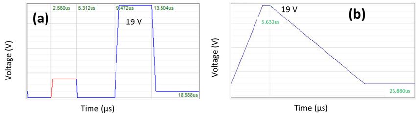
Micromachines 2020, 11, 490 6 of 11
Micromachines 2020, 11, 490 6 of 11
3.3. Generation of ZnO by Joule Heating
3.3. Thermogravimetric
Generation of ZnO by Joule Heating
analysis (TGA) was utilized to investigate the calcination of the precursor
and formation of ZnO byanalysis
Thermogravimetric high-temperature treatment,
(TGA) was utilized which could
to investigate be cataloged
the calcination intoprecursor
of the two stages:
the
andvaporization
formation ofstage
ZnO and the decomposition
by high-temperature of zinc which
treatment, precursor stage
could [26]. Figure
be cataloged into6two
shows thethe
stages: result
ofvaporization
thermal analysis of zinc
stage and the acetate dihydrate
decomposition in ambient
of zinc precursor air. When
stage [26].temperature
Figure 6 shows raising from of
the result 60 to
100 ◦ C, water vaporization occurs, which could be correlated to the sharp decline of the salt weight
thermal analysis of zinc acetate dihydrate in ambient air. When temperature raising from 60 to 100 °C,
ofwater
15% vaporization
in TGA result. There
occurs, is acould
which slightbedecay fromto150
correlated theto ◦ C, which
200 decline
sharp denotes
of the the starting
salt weight of 15% of
in TGA result. There
decomposition is a slight
process. From decay
200 C,◦ from 150istoa200
there °C, which denotes
considerable reductionthe starting
of weightof decomposition
as the reaction is
process. From
promoted 200 °C, there
by temperature. Theis weight
a considerable
is stablereduction of weight
at approximately 23%as after 370 ◦ C, is
the reaction promotedthat
indicating by the
temperature. The weight is stable at approximately 23% after 370 °C, indicating
thermo-decomposition has completed and most of zinc salt has been transformed to ZnO. Although this that the thermo-
decomposition
result recommends has that
completed and most
temperature of zinc
of above 370salt
◦ Chas been transformed
is necessary to thoroughlyto ZnO. Althoughthe
decompose thiszinc
result recommends that temperature of above 370 °C is necessary to thoroughly
precursor, it also suggests that lower temperature still could partially form ZnO. Starting with zinc decompose the zinc
precursor,
acetate it also the
dihydrate, suggests thatislower
reaction temperature
finished with moststill could
of the partially
products ofform ZnO. Starting
the process with zinc
are volatile, such as
acetate dihydrate, the reaction is finished with most of the products
water, acetone ((CH3 )2 CO), acetic acid (CH2 COOH), and carbon dioxide (CO2 ) [27]. of the process are volatile, such
as water, acetone ((CH3)2CO), acetic acid (CH2COOH), and carbon dioxide (CO2) [27].
Figure 6. Thermogravimetric analysis (TGA) survey of zinc precursor in the air to study the formation
Figure 6. Thermogravimetric analysis (TGA) survey of zinc precursor in the air to study the formation
of ZnO.
of ZnO.
Elemental and morphological studies of the heat-treated film could provide more evidence for the
Elemental and morphological studies of the heat-treated film could provide more evidence for
mechanism of the generation of ZnO. Because the decomposition reaction of zinc acetate dihydrate
the mechanism of the generation of ZnO. Because the decomposition reaction of zinc acetate
shows the loss
dihydrate of oxygen
shows the loss element
of oxygen viaelement
productvia vaporization, an investigation
product vaporization, of Zn:O atomic
an investigation of Zn:O ratio
would
atomic ratio would be meaningful for tracking the formation of ZnO. Using EDS analysis, which is in
be meaningful for tracking the formation of ZnO. Using EDS analysis, which is shown
Table
shownA1in (Appendix
Table A1 A), it was found
(Appendix A), it that
wasthe as-printed
found that thefilm exhibitsfilm
as-printed an average
exhibits Zn:O atomicZn:O
an average ratio of
0.378. In the case of using 4-W Joule heating, the atomic ratio of 0.588 could be
atomic ratio of 0.378. In the case of using 4-W Joule heating, the atomic ratio of 0.588 could be observed. This Zn:O
atomic ration further increases to 0.605 when 5-W heating power was applied.
observed. This Zn:O atomic ration further increases to 0.605 when 5-W heating power was applied.The rise of Zn:O atomic
ratio
The isrise
an of
important evidence
Zn:O atomic of an
ratio is thermal decomposition
important evidence ofreaction
thermal and the formation
decomposition of ZnO
reaction andbythe
Joule
heating.
formation It could
of ZnObeby
seen thatheating.
Joule the Zn:O atomic
It could beratio
seenisthat
notthe
significantly
Zn:O atomic different
ratio isbetween 4- and 5-W
not significantly
different
heating between
power. 4- and 5-Wthere
Furthermore, heating power. Furthermore,
is a noticeable variation inthere is a noticeable
this atomic variation inthrough
ratio investigation this
atomic
the ratio
pattern, investigation
which through thetopattern,
could be contributed whichof could
the grading be contributed
temperature through the to the grading of
surface.
temperature
Furthermore,through the surface. study depicts a remarkable change in film structure after Joule
morphological
heating Furthermore, morphological
process (Figure 7). Figure 7a study depicts a remarkable
demonstrates change in
the zinc precursor film
film structure
before aftertreatment
any heat Joule
heating process (Figure 7). Figure 7a demonstrates the zinc precursor film before any heat
was applied. The film appears to be full of fractures, which could be the result of the solvent evaporation treatment
wasthe
and applied. The film
condensation appears
of salt. Thereto are
be remarkable
full of fractures,
changeswhich could
in film be the result
morphology afterof
thethe solvent
Joule heating
evaporation and the condensation of salt. There are remarkable changes in film morphology
treatment, such as the vanishing of notable fractures and the appearance of wrinkles on the surface after the
Joule heating treatment, such as the vanishing of notable fractures and the appearance of wrinkles on
of the film (Figure 7b,c). However, there is no significant difference between these two treated films.
the surface of the film (Figure 7b,c). However, there is no significant difference between these two
These film structures are commonly observed in the sol-gel derived film as our previous report [3].
treated films. These film structures are commonly observed in the sol-gel derived film as our previous
These wrinkles could be originated from the internal stress of film during rapid solvent withdrawal,
report [3]. These wrinkles could be originated from the internal stress of film during rapid solventMicromachines 2020, 11, 490 7 of 11
Micromachines 2020, 11, 490 7 of 11
caused by the difference in thermal expansion of the gelation and underlying layer [28]. In addition,
withdrawal,
the transition fromcaused by the
viscous to difference in thermal
viscoelastic expansion
of the zinc of the
precursor gelation
ink and underlying
also contributes layer
to the [28].
formation of
In addition, the transition from viscous to viscoelastic of the zinc precursor ink also contributes to the
these wrinkles [29].
formation of these wrinkles [29].
Figure 7. Energy-dispersive X-ray spectroscopy (EDS) analysis of zinc precursor film with different
Figureconditions:
treatment 7. Energy-dispersive X-ray
(a) 0 W, (b) 4 W,spectroscopy (EDS)
(c) 5 W. Insets areanalysis
FE–SEMofimages
zinc precursor film with different
of film morphology according
treatment conditions: (a) 0 W, (b) 4 W, (c) 5 W. Insets are FE–SEM images of film morphology
to each condition.
according to each condition.
3.4. UV Light Sensing Performance of the Sensor
3.4. UV Light Sensing Performance of the Sensor
The sensing of UV light was demonstrated by the fabricated device and the result was presented in
The sensing of UV light was demonstrated by the fabricated device and the result was presented
Figure 8. A bias voltage of 5 V was applied to the two terminals of device, which also serves as electrode
in Figure 8. A bias voltage of 5 V was applied to the two terminals of device, which also serves as
by making metal contacts with the semiconductor film. The electrical current was recorded while
electrode by making metal contacts with the semiconductor film. The electrical current was recorded
the UV light
while thewas turned
UV light wason/off
turned(Figure 8a). It 8a).
on/off (Figure could be noted
It could thatthat
be noted thethe
sample
samplewithout
withoutapplying
applying heat
treatment did not shows
heat treatment did nota notable
shows a response to UV light.
notable response to UVOn theOn
light. other
the hand, sample
other hand, with the
sample withtreatment
the
exhibits remarkable
treatment response
exhibits to the
remarkable short-wavelength
response light. Whenlight.
to the short-wavelength UV When
was turn
UV on,
wasthe current
turn on, theraised
significantly until significantly
current raised it reached the equilibrium.
until it reached the On the other hand,
equilibrium. On thewhen
other UV
hand,was turned
when off,turned
UV was the current
off, the current quickly decay to the initial value. It is also worth noting that there is
quickly decay to the initial value. It is also worth noting that there is a remarkable difference of the a remarkable
difference
samples of the samples
with different heatingwith differentsuch
conditions, heating conditions,
as the such aswith
sample treated the sample treated
5-W power haswith 5-W
photocurrent
power has photocurrent with a maximum
−7 value of 1.6 × 10 −7 A, which is about ten times higher than
with a maximum value of 1.6 × 10 A, which is about ten times higher than that of the sample treated
that of the sample treated with 4-W power.
with 4-W power.
The responsivity could be calculated using following expression: [30]
Jph
R= (2)
PS
where Jph is the photocurrent, P is the light intensity, and S is the effective area, which could be
determined by the area of the ZnO pattern between two electrodes, such as 0.2 mm × 0.6 mm.
Further analysis shows the responsivity values at 5.42 mW/cm2 light intensity of the 5-W sample and
the 4-W sample is 0.029 and 0.0027 A/W, respectively. Although the responsivity is lower than that
has been reported in other inkjet-printed ZnO-based UV photodetector [31], it could be due to the
obtained temperature is lower than the point where the reaction is totally finished. In Figure 8b, the I–V
characteristics of prepared devices were presented, which show a linear current–voltage relationshipMicromachines 2020, 11, 490 8 of 11
for both of the devices
Micromachines with treatment. This behavior indeed shows the Ohmic contact nature of
2020, 11, 490 8 ofthe
11
silver–ZnO interface.
Figure 8. Photo-sensing properties of the fabricated device. (a) Sequential illumination of the sensor by
Figure 8. Photo-sensing properties of the fabricated device. (a) Sequential illumination of the sensor
UV light and obtained photocurrent. (b) I–V curve of the devices under UV illumination.
by UV light and obtained photocurrent. (b) I–V curve of the devices under UV illumination.
4. Discussion
The responsivity could be calculated using following expression: [30]
The photosensitivity of the device is strongly influenced by the heat treatment condition. As the
discussion in previous section has pointed out, temperature of higher than 150 ◦ C is critical to facilitate (2)
,
the reaction to form ZnO from the zinc salt. It is worth noting that photosensitivity is a common
where Jphof
characteristic is athe photocurrent, PZnO
semiconductor. is theis light
a wide intensity,
bandgap andsemiconductor
S is the effective (Eg = 3.35
area, which
eV could be
at room
determined
temperature by the
[32]). area of the
Therefore, it ZnO
onlypattern between
be sensitive twolarger
with electrodes,
photonsuch as 0.2 mm
energy × 0.6
of the mm. Further
incident light,
analysis shows the responsivity values at 5.42 mW/cm 2 light intensity of the 5-W sample and the 4-
such as the UV light used in this work which has photon energy of 3.40 eV according to 365 nm central
W sample
wavelength is 0.029
of the LED.and 0.0027 A/W, respectively. Although the responsivity is lower than that has
been reported
The sample without in other inkjet-printed
heat treatment could ZnO-based
not form UVZnO photodetector
by the thermal[31], decomposition
it could be dueprocess.
to the
obtained temperature is lower than the point where the reaction is totally finished. In Figure 8b, the
Therefore, the prepared film failed to work as a photodetector. Meanwhile, the sample processed with
I–V characteristics of prepared devices were presented, which show a linear current–voltage
4-W power demonstrates a remarkable response to UV illumination. It is because the temperature
relationship for both of the devices with treatment. This behavior indeed shows the Ohmic contact
generated by the Joule heating process has facilitated the formation of ZnO semiconductor. As a
nature of the silver–ZnO interface.
wide bandgap semiconductor, the interaction of ZnO crystalline with high energy photons excites
the generation
4. Discussion of the electron-hole pair which increases the carrier concentration in the lattice [33].
Therefore, film resistance reduces and causes a surge in current running through the device.
The photosensitivity of the device is strongly influenced by the heat treatment condition. As the
Furthermore, the sample processed with 5-W power possesses a better performance in terms
discussion in previous section has pointed out, temperature of higher than 150 °C is critical to
of responsivity to UV light. This improvement indicates that the magnitude of input power for
facilitate the reaction to form ZnO from the zinc salt. It is worth noting that photosensitivity is a
Joule heating of semiconductor film could significantly influence the film properties. The root of
common characteristic of a semiconductor. ZnO is a wide bandgap semiconductor (Eg = 3.35 eV at
this enhancement could be originated from the fact that higher temperatures could promote more
room temperature [32]). Therefore, it only be sensitive with larger photon energy of the incident light,
formation of ZnO as previous discussion, therefore the interaction with photon is improved and
such as the UV light used in this work which has photon energy of 3.40 eV according to 365 nm
morecentral
electron-hole
wavelength pairs could
of the LED.be generated when exposing to the UV illumination. In addition,
higher temperatures
The sample without heatimprove
could also treatmentthe contact
could between
not form ZnO byZnOthenanoparticles, thereforeprocess.
thermal decomposition reduce
the band bending
Therefore, the at the interfaces
prepared andtopromote
film failed work asthe transportationMeanwhile,
a photodetector. of electronthe through
samplethose grain
processed
boundaries [30].
with 4-W power demonstrates a remarkable response to UV illumination. It is because the
Current workgenerated
temperature employed silicon
by thewaferJouledue to its excellent
heating processheathasresistance,
facilitatedbecause of the temperature
the formation of ZnO
during Joule heating ◦
semiconductor. Ascould
a wideexcess 250 semiconductor,
bandgap C, which mostthe of interaction
polymer will not be
of ZnO able to withstand.
crystalline with high
One possible alternative
energy photons solution
excites the isgeneration
using high of temperature polymerpair
the electron-hole such which
as polyimide.
increasesHowever, due
the carrier
concentration in the lattice [33]. Therefore, film resistance reduces and causes
to the low thermal conductivity of polyimide comparing that of silicon wafer [34,35], the structure of a surge in current
running
device must be through
changed the to
device.
reduce the distance from heater to the printed zinc salt in order to obtain a
sufficientFurthermore,
calcination. the sample processed with 5-W power possesses a better performance in terms of
responsivity to UV light. This improvement indicates that the magnitude of input power for Joule
5. Conclusions
heating of semiconductor film could significantly influence the film properties. The root of this
enhancement could be originated from the fact that higher temperatures could promote more
In this work, on-substrate heating synthesis of ZnO thin film by the printed silver resistive
formation of ZnO as previous discussion, therefore the interaction with photon is improved and more
heater is proposed. Both conductive patterns and the precursor pattern were printed on only one
electron-hole pairs could be generated when exposing to the UV illumination. In addition, higher
inkjet printer with an exchange of cartridge for each material. Electrical current running through the
temperatures could also improve the contact between ZnO nanoparticles, therefore reduce the bandthe structure of device must be changed to reduce the distance from heater to the printed zinc salt in
order to obtain a sufficient calcination.
5. Conclusions
Micromachines 2020, 11,
In this work, 490
on-substrate 9 of 11
heating synthesis of ZnO thin film by the printed silver resistive heater
is proposed. Both conductive patterns and the precursor pattern were printed on only one inkjet
printer with an exchange
silver conductive patternofgenerates
cartridgeheat,
for each
whichmaterial. Electrical
is utilized current
to facilitate therunning
thermalthrough the silverof
decomposition
conductive pattern generates heat, which is utilized to facilitate the thermal decomposition
printed zinc precursor film to form ZnO. The magnitude of supplied power for heating process of printed
has
zinc precursor film to form ZnO. The magnitude of supplied power for heating process
significant influence on the film formation via the achieved temperature. Therefore, it is found that has significant
influence on the
higher power film produce
could formation via theproperty
a better achievedoftemperature.
printed ZnOTherefore,
semiconductorit is found that higher
film. Despite power
the humble
could produce a better property of printed ZnO semiconductor film. Despite the humble
performance of printed photodetector, this work demonstrates a promising approach to additively performance
ofmanufacture
printed photodetector, this work
electronic devices, demonstrates
which reduces theanumber
promising approach involved
of equipment to additively manufacture
and the amount of
electronic devices, which reduces the number of equipment
energy consumed. Hence, integrated 3D printing might also be possible. involved and the amount of energy
consumed. Hence, integrated 3D printing might also be possible.
Author Contributions: Conceptualization, V.-T.T. and H.D.; methodology, V.-T.T. and Y.W.; formal analysis, V.Y.T.;
Author Contributions:
investigation, Conceptualization,
V.-Y.T. and V.-T.T. draft
Y.W.; writing—original and H.D.; methodology,
preparation, V.-T.T.; V.-T.T. and Y.W.;and
writing—review formal analysis,
editing, H.D.;
V.Y.T.;
visualization, V.-T.T.; supervision, H.D.; project administration, H.D. All authors have read and agreed toand
investigation, V.-Y.T. and Y.W.; writing—original draft preparation, V.-T.T.; writing—review the
editing,
publishedH.D.; visualization,
version V.-T.T.; supervision, H.D.; project administration, H.D. All authors have read and
of the manuscript.
agreed to the
Funding: published
This researchversion of theby
was funded manuscript
Ministry of Education Academic Research Fund, Singapore.
Funding: This research
Acknowledgments: Wewas funded by
appreciate theMinistry
equipmentof Education Academic
support from Research
Singapore CentreFund,
for 3DSingapore.
Printing (SC3DP).
Acknowledgments: We
Conflicts of Interest: appreciate
The the equipment
authors declare support
no conflict from Singapore Centre for 3D Printing (SC3DP).
of interest.
Conflicts of Interest: The authors declare no conflict of interest.
Appendix A
Appendix A
Table A1. EDS Investigation of Zn:O atomic ration at random positions on printed pattern.
Table A1. EDS Investigation of Zn:O atomic ration at random positions on printed pattern.
Zn:O Atomic Ratio
Location 1 2 3 4 Zn:O Atomic
5 Ratio
6 Average Standard Deviation
Location 1 2 3 4 5 6 Average Standard Deviation
0W 0.430 0.431 0.422 0.390 0.292 0.305 0.378 0.058
0W 0.430 0.431 0.422 0.390 0.292 0.305 0.378 0.058
4W 0.536 0.545 0.504 0.705 0.681 0.557 0.588 0.076
5W 4 W 0.553
0.536 0.567
0.545 0.504
0.517 0.705
0.691 0.681
0.651 0.557
0.648 0.5880.605 0.0760.062
5W 0.553 0.567 0.517 0.691 0.651 0.648 0.605 0.062
Figure A1. Waveform of signal applying to cartridge nozzles to create jetting of ink: (a) silver ink and
Figure A1.
Micromachines Waveform of signal applying to cartridge nozzles to create jetting of ink: (a) silver ink and10 of 11
(b) zinc2020, 11, 490
salt ink.
(b) zinc salt ink.
Figure
FigureA2.
A2.Low-magnification
Low-magnificationFE–SEM
FE–SEMimages
imagesof
oftwo
twosamples
samplesbefore
before(a)
(a)and
andafter
afterheat
heattreatment
treatment(b).
(b).
References
1. Zhan, Z.; An, J.; Wei, Y.; Tran, V.T.; Du, H. Inkjet-printed optoelectronics. Nanoscale 2017, 9, 965–993,
doi:10.1039/C6NR08220C.
2. Nayak, L.; Mohanty, S.; Nayak, S.K.; Ramadoss, A. A review on inkjet printing of nanoparticle inks forMicromachines 2020, 11, 490 10 of 11
References
1. Zhan, Z.; An, J.; Wei, Y.; Tran, V.T.; Du, H. Inkjet-printed optoelectronics. Nanoscale 2017, 9, 965–993.
[CrossRef]
2. Nayak, L.; Mohanty, S.; Nayak, S.K.; Ramadoss, A. A review on inkjet printing of nanoparticle inks for
flexible electronics. J. Mater. Chem. C 2019, 7, 8771–8795. [CrossRef]
3. Tran, V.-T.; Wei, Y.; Yang, H.; Zhan, Z.; Du, H. All-inkjet-printed flexible ZnO micro photodetector for a
wearable UV monitoring device. Nanotechnology 2017, 28, 095204. [CrossRef]
4. Yus, J.; Gonzalez, Z.; Sanchez-Herencia, A.J.; Sangiorgi, A.; Sangiorgi, N.; Gardini, D.; Sanson, A.; Galassi, C.;
Caballero, A.; Morales, J.; et al. Semiconductor water-based inks: Miniaturized NiO pseudocapacitor
electrodes by inkjet printing. J. Eur. Ceram. Soc. 2019, 39, 2908–2914. [CrossRef]
5. Sanchez, J.G.; Balderrama, V.S.; Garduno, S.I.; Osorio, E.; Viterisi, A.; Estrada, M.; Ferre-Borrull, J.; Pallares, J.;
Marsal, L.F. Impact of inkjet printed ZnO electron transport layer on the characteristics of polymer solar cells.
RSC Adv. 2018, 8, 13094–13102. [CrossRef]
6. Ganesan, S.; Gollu, S.R.; Alam khan, J.; Kushwaha, A.; Gupta, D. Inkjet printing of zinc oxide and P3HT:ICBA
in ambient conditions for inverted bulk heterojunction solar cells. Opt. Mater. 2019, 94, 430–435. [CrossRef]
7. Hasan, K.u.; Nur, O.; Willander, M. Screen printed ZnO ultraviolet photoconductive sensor on pencil drawn
circuitry over paper. Appl. Phys. Lett. 2012, 100, 211104. [CrossRef]
8. Liang, Y.N.; Lok, B.K.; Wang, L.; Feng, C.; Lu, A.C.W.; Mei, T.; Hu, X. Effects of the morphology of
inkjet printed zinc oxide (ZnO) on thin film transistor performance and seeded ZnO nanorod growth.
Thin Solid Films 2013, 544, 509–514. [CrossRef]
9. Jiang, L.; Li, J.; Huang, K.; Li, S.; Wang, Q.; Sun, Z.; Mei, T.; Wang, J.; Zhang, L.; Wang, N.; et al.
Low-Temperature and Solution-Processable Zinc Oxide Transistors for Transparent Electronics. ACS Omega
2017, 2, 8990–8996. [CrossRef]
10. Friedmann, D.; Lee, A.F.; Wilson, K.; Jalili, R.; Caruso, R.A. Printing approaches to inorganic semiconductor
photocatalyst fabrication. J. Mater. Chem. A 2019, 7, 10858–10878. [CrossRef]
11. Gagnon, J.C.; Presley, M.; Le, N.Q.; Montalbano, T.J.; Storck, S. A pathway to compound semiconductor
additive manufacturing. MRS Commun. 2019, 9, 1001–1007. [CrossRef]
12. Chae, D.; Kim, J.; Shin, J.; Lee, W.H.; Ko, S. A low-temperature and short-annealing process for metal oxide
thin film transistors using deep ultraviolet light for roll-to-roll processing. Curr. Appl. Phys. 2019, 19, 954–960.
[CrossRef]
13. Jeon, J.B.; Kim, B.J.; Bang, G.J.; Kim, M.-C.; Lee, D.G.; Lee, J.M.; Lee, M.; Han, H.S.; Boschloo, G.; Lee, S.; et al.
Photo-annealed amorphous titanium oxide for perovskite solar cells. Nanoscale 2019, 11, 19488–19496.
[CrossRef]
14. Palneedi, H.; Park, J.H.; Maurya, D.; Peddigari, M.; Hwang, G.-T.; Annapureddy, V.; Kim, J.-W.; Choi, J.-J.;
Hahn, B.-D.; Priya, S.; et al. Laser Irradiation of Metal Oxide Films and Nanostructures: Applications and
Advances. Adv. Mater. 2018, 30, 1705148. [CrossRef]
15. Sharma, S.; Pande, S.S.; Swaminathan, P. Top-down synthesis of zinc oxide based inks for inkjet printing.
RSC Adv. 2017, 7, 39411–39419. [CrossRef]
16. Rao, A.; Long, H.; Harley-Trochimczyk, A.; Pham, T.; Zettl, A.; Carraro, C.; Maboudian, R. In Situ Localized
Growth of Ordered Metal Oxide Hollow Sphere Array on Microheater Platform for Sensitive, Ultra-Fast Gas
Sensing. ACS Appl. Mater. Interfaces 2017, 9, 2634–2641. [CrossRef]
17. Yan, H.; Wu, H. Joule Heating and Chip Materials. In Encyclopedia of Microfluidics and Nanofluidics; Li, D., Ed.;
Springer: Boston, MA, USA, 2013.
18. Nguyen, H.; Quy, C.T.; Hoa, N.D.; Lam, N.T.; Duy, N.V.; Quang, V.V.; Hieu, N.V. Controllable growth of
ZnO nanowires grown on discrete islands of Au catalyst for realization of planar-type micro gas sensors.
Sens. Actuators Chem. 2014, 193, 888–894. [CrossRef]
19. Long, H.; Turner, S.; Yan, A.; Xu, H.; Jang, M.; Carraro, C.; Maboudian, R.; Zettl, A. Plasma assisted formation
of 3D highly porous nanostructured metal oxide network on microheater platform for Low power gas
sensing. Sens. Actuators Chem. 2019, 301, 127067. [CrossRef]
20. Dai, C.-L. A capacitive humidity sensor integrated with micro heater and ring oscillator circuit fabricated by
CMOS–MEMS technique. Sens. Actuators Chem. 2007, 122, 375–380. [CrossRef]Micromachines 2020, 11, 490 11 of 11
21. Nerushev, O.A.; Ek-Weis, J.; Campbell, E.E.B. In situ studies of growth of carbon nanotubes on a local metal
microheater. Nanotechnology 2015, 26, 505601. [CrossRef]
22. Kwon, J.; Hong, S.; Kim, G.; Suh, Y.D.; Lee, H.; Choo, S.-Y.; Lee, D.; Kong, H.; Yeo, J.; Ko, S.H. Digitally
patterned resistive micro heater as a platform for zinc oxide nanowire based micro sensor. Appl. Surf. Sci.
2018, 447, 1–7. [CrossRef]
23. Tran, V.-T.; Wei, Y.; Liau, W.; Yang, H.; Du, H. Preparing of Interdigitated Microelectrode Arrays for
AC Electrokinetic Devices Using Inkjet Printing of Silver Nanoparticles Ink. Micromachines 2017, 8, 106.
[CrossRef]
24. Ravindra, N.M.; Abedrabbo, S.; Wei, C.; Tong, F.M.; Nanda, A.K.; Speranza, A.C. Temperature-dependent
emissivity of silicon-related materials and structures. IEEE Tran. Semicond. Manuf. 1998, 11, 30–39. [CrossRef]
25. Lee, S.M.; Dyer, D.C.; Gardner, J.W. Design and optimisation of a high-temperature silicon micro-hotplate for
nanoporous palladium pellistors. Microelectron. J. 2003, 34, 115–126. [CrossRef]
26. Paraguay D, F.; Estrada L, W.; Acosta N, D.R.; Andrade, E.; Miki-Yoshida, M. Growth, structure and optical
characterization of high quality ZnO thin films obtained by spray pyrolysis. Thin Solid Films 1999, 350,
192–202. [CrossRef]
27. Lin, C.-C.; Li, Y.-Y. Synthesis of ZnO nanowires by thermal decomposition of zinc acetate dihydrate.
Mater. Chem. Physi. 2009, 113, 334–337. [CrossRef]
28. Kwon, S.J.; Park, J.-H.; Park, J.-G. Wrinkling of a sol-gel-derived thin film. Phys. Rev. E 2005, 71, 011604.
[CrossRef]
29. Justin Raj, C.; Karthick, S.N.; Hemalatha, K.V.; Kim, S.-K.; Kim, B.C.; Yu, K.-H.; Kim, H.-J. Synthesis of
self-light-scattering wrinkle structured ZnO photoanode by sol–gel method for dye-sensitized solar cells.
Appl. Phys. A 2014, 116, 811–816. [CrossRef]
30. Liu, X.; Gu, L.; Zhang, Q.; Wu, J.; Long, Y.; Fan, Z. All-printable band-edge modulated ZnO nanowire
photodetectors with ultra-high detectivity. Nat. Commun. 2014, 5. [CrossRef]
31. Dong, Y.; Zou, Y.; Song, J.; Li, J.; Han, B.; Shan, Q.; Xu, L.; Xue, J.; Zeng, H. An all-inkjet-printed flexible UV
photodetector. Nanoscale 2017, 9, 8580–8585. [CrossRef]
32. Monroy, E.; Omnès, F.; Calle, F. Wide-bandgap semiconductor ultraviolet photodetectors.
Semicond. Sci. Technol. 2003, 18, R33. [CrossRef]
33. Petritz, R.L. Theory of Photoconductivity in Semiconductor Films. Phys. Rev. 1956, 104, 1508–1516. [CrossRef]
34. Benford, D.J.; Powers, T.J.; Moseley, S.H. Thermal conductivity of Kapton tape. Cryogenics 1999, 39, 93–95.
[CrossRef]
35. Hopkins, P.E.; Reinke, C.M.; Su, M.F.; Olsson, R.H.; Shaner, E.A.; Leseman, Z.C.; Serrano, J.R.; Phinney, L.M.;
El-Kady, I. Reduction in the Thermal Conductivity of Single Crystalline Silicon by Phononic Crystal Patterning.
Nano Lett. 2011, 11, 107–112. [CrossRef]
© 2020 by the authors. Licensee MDPI, Basel, Switzerland. This article is an open access
article distributed under the terms and conditions of the Creative Commons Attribution
(CC BY) license (http://creativecommons.org/licenses/by/4.0/).You can also read