Polymer-assisted TEM specimen preparation method for oxidation-sensitive 2D materials - Uni Ulm
←
→
Page content transcription
If your browser does not render page correctly, please read the page content below
Nanotechnology

PAPER

Polymer-assisted TEM specimen preparation method for oxidation-
sensitive 2D materials
To cite this article: Janis Köster et al 2021 Nanotechnology 32 075704

View the article online for updates and enhancements.

                             This content was downloaded from IP address 134.60.120.216 on 19/01/2021 at 10:16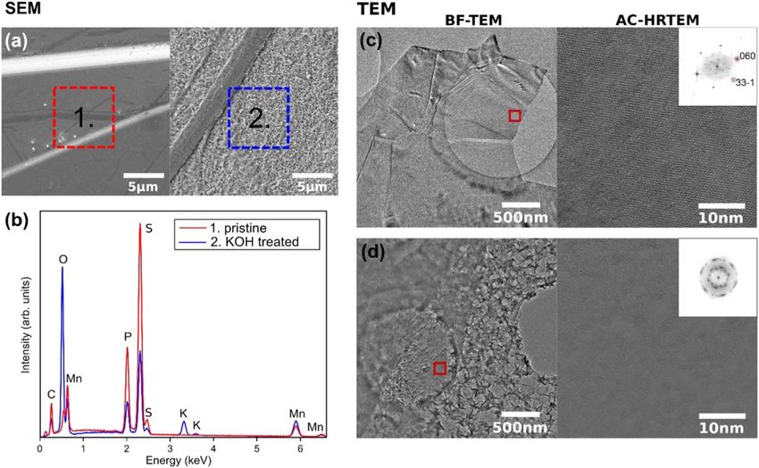
Nanotechnology

Nanotechnology 32 (2021) 075704 (6pp)                                                             https://doi.org/10.1088/1361-6528/abc49e

Polymer-assisted TEM specimen
preparation method for oxidation-sensitive
2D materials
Janis Köster1 , Baokun Liang1 , Alexander Storm and Ute Kaiser
Electron Microscopy Group of Materials Science, Ulm University, Albert-Einstein-Allee 11, D-89081 Ulm,
Germany

E-mail: ute.kaiser@uni-ulm.de

Received 11 August 2020, revised 8 October 2020
Accepted for publication 26 October 2020
Published 24 November 2020

Abstract
By structural and analytical TEM and scanning electron microscopy experiments we show that
atomically-resolved structural characterization of oxidation-sensitive two-dimensional material is
strongly hindered when the final step of the preparation process, the transfer to the TEM grid, is
performed with a wet etching method involving bases or acids, interacting with the highly
reactive sample surface. Here we present an alternative polymer-assisted and mechanical-
exfoliation-based sample preparation method and demonstrate it on selected oxidation-sensitive
transition metal phosphorus trisulfides and transition metal dichalcogenides. The analysis,
obtained from the samples prepared with both of the methods clearly show that oxidation is the
origin of discrepancy, the oxidation during the final preparation step is strongly reduced only
when the new method is applied, and atomically-resolved structural characterization of the
pristine structures is now possible.
Supplementary material for this article is available online

Keywords: 2D material, HRTEM, TMPT, TMD, oxidation-sensitive, specimen preparation
(Some figures may appear in colour only in the online journal)

1. Introduction                                                        preparation methods were applied for 2D materials: standard
                                                                       transfer with polymer [13], direct transfer for the case of
Nowadays, the number of two-dimensional (2D) materials is              graphene [14], polyimide-assisted transfer for the case of
fast-growing and transition metal phosphorous trisulfides               h-BN [15], liquid exfoliation [16], and scotch tape method
(TMPTs) are one of the new-born stars due to their magnetic            with potassium hydroxide (KOH). In the following, the
and electric properties [1–3], allocating them as promising            scotch tape method with potassium hydroxide will be referred
candidates for future heterostructure devices [4–6], for               to as the ‘KOH method’ [17]. The KOH method is an
instance, combined with members of the material class of               effective method to transfer the flake of interest with pre-
transition metal dichalcogenides (TMDs) [7]. Aberration-               determined thickness to a certain position on the TEM grid,
corrected high-resolution transmission electron microscopy             and therefore commonly used in the TEM community. As the
(AC-HRTEM) offers a powerful approach to analyse and                   KOH method is conducted in an ambient atmosphere and
modify freestanding thin samples at the atomic scale [8–12].           involves a highly reactive chemical, in this preparation pro-
However, surface contamination and oxidation hinder the                cess chemical reactions take place and consequently structural
analysis of the material in its pristine state. Thus, the fabri-       decomposition occurs [18, 19]. Therefore, TEM imaging of
cation of high-quality TEM samples is of fundamental                   the atomic structure of oxidation-sensitive TMPTs and
importance. In previous studies, many different sample                 TMDs, when prepared with the KOH method, is very diffi-
                                                                       cult. To prevent the materials from oxidation during TEM
1
    These authors contributed equally to this work.                    preparation, a stamping method conducted in an oxygen-free

0957-4484/21/075704+06$33.00                                       1                            © 2020 IOP Publishing Ltd Printed in the UK
Nanotechnology 32 (2021) 075704 J Köster et al
Figure 1. Step by step polymer-assisted preparation of a freestanding TEM sample without base or acid. The substrate is a Si/SiO2 wafer
coated with polyvinyl alcohol (PVA) or poly (methyl methacrylate) (PMMA) (shown in I and II). First, the bulk material is thinned down by
mechanical exfoliation with scotch tape. By pressing the scotch tape on the wafer (depiction III), the material flakes are deposited on the
polymer layer (depiction IV). Subsequently, thin flakes can be identified with an optical microscope. For calculating the contrast of thin
layers on a semi-infinite Si substrate covered with a SiO2—PVA/PMMA layer, a theoretical model based on the Fresnel equation was used
[22] (see figure S1). In step V, the TEM grid is brought into contact with the wafer by applying water or IPA, depending on the applied
polymer layer. Evaporation and adhesion force of the liquid brings the flexible carbon mesh membrane of the TEM grid in contact with the
polymer layer. Further, the grid is removed by dissolving the polymer layer (shown in VI). Type 1 (Ultrapure) water is used in the case of a
PVA layer and acetone or anisole in the case of PMMA. In VII the TEM grid with deposited material flakes is illustrated.
environment was developed [20, 21]. This method allows to layer is dissolved, the grid floats on the liquid drop and can be
prepare single-layers of oxidation-sensitive 2D materials. gently removed by tweezers. This process prevents the mat-
However, it faces the challenge of transferring a freestanding erial from contacting with acids or bases.
material flake to a TEM grid.
Here we propose a new polymer-assisted method for
oxidation-sensitive 2D materials performed under ambient
conditions, which minimizes oxidation and allows a con- 3. Results and analysis
trolled transfer to the TEM grid (see figure S1, available
online at stacks.iop.org/NANO/32/075704/mmedia). This In the following, the performance in the sample quality of the
method is exemplarily performed on FePS3, MnPS3, polymer-assisted method is analysed and compared to the
1T-TiSe2, and 2H-NbSe2. In addition, the method maintains KOH method. We start by testing the effect of the KOH
the possibility to determine the sample thickness (single-layer solution on the surface morphology and chemistry of KOH-
or few-layer) before the transfer process. treated and untreated bulk MnPS3 flakes using scanning
electron microscopy (SEM). In figure 2(a), SEM images of
pristine MnPS3 are presented on the left side and after contact
with KOH solution on the right side. Dramatic changes in the
2. Proposed sample preparation method surface morphology, for example increased roughness, are
visible. In figure 2(b), the corresponding energy-dispersive
Figure 1 illustrates the preparation process in detail. Our x-ray (EDX) spectra are shown in the energy range of 0–6.6
preparation process starts with thinning down the bulk mat- keV taken from the red-framed and blue-framed areas in
erial by the established mechanical exfoliation technique. The figure 2(a). The two spectra show similarities as in both
resulting flakes are then deposited on a polymer-coated spectra carbon (C-Kα=0.277 keV) and oxygen (O-
Si/SiO2 wafer in which the polymer layer can be either PVA Kα=0.525 keV) signals are visible. These peaks may ori-
or PMMA. To bring the underlying polymer layer and the ginate from the SEM sample fabrication process, which was
sample in contact with the TEM grid, the grid is fixed using a performed in air. However, strong differences can be
metal or glass tip and wetted from the outside by a drop of observed in the untreated sample (red curve), the maximum
isopropyl alcohol (IPA) or water, depending on the polymer peak ratios of the oxygen peak with respect to the manganese
layer used. Due to the evaporation of the liquids, the flexible (Mn-Kα=5.900 keV; Mn-Lα=0.637 keV), sulfur (S-
carbon mesh membrane of the TEM grid is directly brought in Kα=2.309 keV), and phosphorous (P-Kα=2.010 keV)
contact with the material flake. Subsequently, the fixing tool peaks of MnPS3 are low, while the ratios in the KOH-treated
(the metal or glass tip) is removed and the underlying polymer case (blue curve) are considerably higher. This indicates a
layer is then dissolved by water in the case of PVA, or by stronger oxidation for MnPS3 after contact with the KOH
acetone if PMMA is used. The most gently way for dissolving solution. Additionally, the peak intensities of the P and S
the PVA or PMMA layer is to drop the liquids right beside the peaks in the blue curve are lowered with respect to the former
grid, such that the dissolving process takes place from the ratios between the metal and the elements P and S (figure S2
edge to the center of the grid. After the underlying polymer provides cross-section SEM images and the corresponding
2
Nanotechnology 32 (2021) 075704 J Köster et al
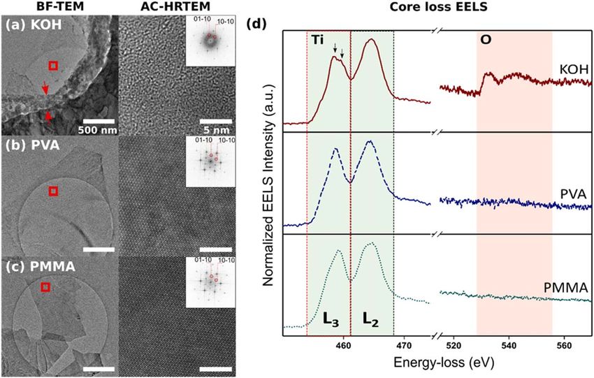
Figure 2. Structural and chemical characterization of bulk (a)–(b) and few-layer MnPS3 (c)–(d). (a) shows SEM images of the surfaces of a
pristine (left) and KOH treated (right) bulk MnPS3 crystal. The marked red and blue squares indicate the corresponding areas for EDX
analysis, spectra are shown in (b). The strong O peak after contact with KOH is the most obvious difference between both spectra. The peak
intensities of the Mn (Kα 5.900 keV/Lα 0.637 keV), S (Kα 2.309 keV), and P (Kα 2.010 keV) are clearly visible in both of the spectra.
However, the S and P peak intensities are strongly reduced after contact with KOH because of materials decomposition. Moreover, a K peak
is only visible in the KOH treated sample. (c) BF-TEM overview image along the [103] zone-axis of few-layer MnPS3 prepared with the
PVA method, the area where the AC-HRTEM image is taken is marked with a red rectangle. The single crystalline nature is clearly visible.
(d) BF-TEM overview image of few-layer MnPS3 prepared with the KOH method, showing heavy damages. From the AC-HRTEM and
corresponding FFT images on the right, we see the polycrystalline nature as well as the high degree of amorphisation, right up to the
formation of holes in the thin layer (results of FePS3 are presented in figure S5).
EDX spectra of bulk FePS3 and MnPS3 after the treatment polymers PVA and PMMA as substrate, respectively. The
with KOH solution). Moreover, a potassium (K) peak (K-Kα intension of applying two polymers is to find out whether the
3.314 keV) becomes visible for the KOH-treated sample. In success of the proposed method is sensitive to the type of the
the next step, we compared a much thinner MnPS3 sample polymer and the different related solvents, water or acetone.
(few-layer MnPS3) prepared with the KOH method and with The results of BF-TEM, AC-HRTEM, and EELS analysis are
the polymer-assisted method using AC-HRTEM (the presented in figure 3 (additional SEM and EDX results are
corresponding structure models are given in figure S3). In the provided in figure S6). By comparing the overview BF-TEM
latter case, the overview BF-TEM image of few-layer MnPS3 images, it is clearly seen that the edge of the flake is not sharp
in figure 2(c) shows an intact flake with sharp edges. The AC- and shows a deterioration in the KOH-treated sample, as
HRTEM image, together with corresponding Fast Fourier highlighted by the two red arrows in figure 3(a). The other
Transform (FFT) patterns, clearly demonstrates the crystalline two samples show sharp edges, see figures 3(b) and (c).
nature of the material. On the contrary, the BF-TEM image of Comparing the AC-HRTEM images and their FFTs placed as
the flake prepared with the KOH method in figure 2(d) shows insets obtained from the red rectangles marked in the
the deterioration of the flake. The corresponding AC-HRTEM corresponding BF-TEM images in figures 3(a)–(c), the dif-
image (taken from the red rectangular in the BF-TEM image) ferences in the atomic structures are obvious. The crystalline
demonstrates the presence of holes and a polycrystalline 1T-TiSe2 atomic structure is shown in the AC-HRTEM
nature of the material, underlined by the corresponding FFT images in figures 3(b) and (c), highlighted by the FFTs (the
patterns in the upper right. Results on FePS3 showed corresponding structure models are given in figure S3). In
amorphisation after the material was treated by the KOH contrast, the AC-HRTEM image of the KOH treated sample
solution as well (see figure S4 and the more detailed in figure 3(a) shows a predominant amorphous structure, as
description of the decomposition process). also seen in the FFT at low spatial frequencies. Furthermore,
To prove the adaptability of the proposed polymer- the chemical information of each sample are revealed in the
assisted preparation method to highly oxidation-sensitive EELS data showing the Ti-L and O-K energy loss edges, see
TMDs, we now study 1T-TiSe2. Two samples of few-layer figure 3(d). An oxygen peak starting at 530 eV is only present
1T-TiSe2 are prepared for TEM investigation using the in the KOH treated sample [23]. Slight oxidation after PVA
3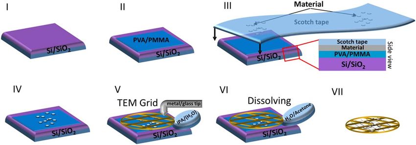
Nanotechnology 32 (2021) 075704 J Köster et al
Figure 3. Comparison of the degree of oxidation in few-layer 1T-TiSe2 prepared by KOH- and polymer-assisted (PVA and PMMA) methods.
Images (a)–(c) show 80 kV overview BF-TEM images on the left (the arrow in (a) marks the edge-contamination) and Cs-corrected HRTEM
images on the right along the [001] zone-axis (with their FFTs as insets), obtained from the red-squared areas in the BF-TEM images. By
comparing the Cs-corrected HRTEM images in (a)–(c), the oxidation of TiSe2 in (a) can be clearly seen. Accordingly, the corresponding
EELS spectra in (d) show that in the case of the KOH method prepared sample, an O peak at 530 eV occurs and a splitting of the Ti-L3 edge
(see the black arrows) originating from oxidation (TiO2 formation) is visible. In the PVA and PMMA method cases, the positions and shapes
of the Ti-L2,3 peaks at 462 and 456 eV show just the edge structure for Ti in 1T-TiSe2 (the raw data of the spectra is given in figure S7).
and PMMA treatment might be expected as well, as they are the higher energy site might be described as a superposition
prepared under ambient conditions. As no O-K peak was of the spectra of the oxide with the pristine 1T-TiSe2 layer.
measured in EELS, the amount of oxidation must at least be Crystalline TiO2 (e.g. anatase and rutile) [27–29] shows a
below the signal to noise ratio for O detection for the settings similar core loss Ti (L2,3) edge fine structure as 1T-TiSe2 but
used to acquire the spectra. shifted by several eV to higher energies [25]. When the outer
Moreover, the changes in the chemical bonding due to layers oxidize and the inner layers of TiSe2 stay intact, a
the oxidation are also visible in the Ti-L3 edges. The Ti superposition of the titanium oxides L3-edge with the
spectra contain bands attributed to the 3d←2p3/2 and 1T-TiSe2 L3-edge would result in the observed spectra [27],
3d←2p1/2 transitions showing up as two main peaks at supplementary information (SI) figures S3 and S5. However,
around 455–463 eV (L3 peak) and 463 eV–470 eV (L2 peak), due to the limited energy resolution, unambiguous identifi-
respectively. The fine structure of the Ti-L2,3 edge is deter- cation of the titanium oxide structure is not possible. Overall,
mined by the chemical composition and structure of the the shown L2,3 edges for the PVA and PMMA samples
material. Crystal field splitting leads in the case of pristine coincide with previous reported Ti-L2,3 edges in pristine
TiSe2 to a splitting of the 3d orbitals to the lower energy t2g 1T-TiSe2 [24, 26, 30]. Moreover, it should be noticed that
and higher energy eg levels [24, 25]. Red and green dotted there is no significant difference between samples prepared
boxes in figure 3(d) highlight the L3 and L2 edges for the via PVA or PMMA.
different TiSe2 samples, respectively. The corresponding We verified the applicability of the polymer-assisted
peaks expected for the transition into the empty t2g and eg sample preparation method to single-layers using another
levels merge due to the limited EELS energy resolution of 0.6 oxidation-sensitive TMD. 2H-NbSe2 was chosen as it exhibits
eV and acquisition at room temperature [24, 26]. As a result, superconducting properties and thus excellent TEM sample
the weaker t2g transition appears as a broad shoulder. In preparation may be crucial for understanding the property’s
figure 3(d), in the case of the KOH prepared sample, the Ti-L3 structural origin [31]. The structural model of 2H-NbSe2 is
peak splits (see black arrows) and an O peak appears thus Ti– shown in figure 4(a). AC-HRTEM experiments were per-
O bonds formed. The process of oxidization can be described formed for single-layer and few-layer 2H-NbSe2 using the
by the formation of TiOxSe2−x and a gradual replacement of Cc/Cs (chromatic and spherical aberration)—corrected
Se by O atoms in the crystal [27]. The split in the L3 peak at SALVE instrument operated at 80 kV (SEM image and EDX
4Nanotechnology 32 (2021) 075704 J Köster et al
Figure 4. Results of a PVA prepared few-layer and single-layer 2H-NbSe2 samples. In (a) the structural model of single-layer 2H-NbSe2 is
shown in top and side view in which selenium atoms are green and niobium atoms are blue colored. (b) and (c) show 80 kV Cc/Cs-corrected
HRTEM images along the [001] zone-axis demonstrating successful sample preparation without deterioration due to oxidation. FFTs are
inserted in the top right corner. A depiction of a selected enlarged region is highlighted by green circles in (c), showing a double Se vacancy
(marked by a red dotted circle).
results see figure S6). As figures 4(b) and (c) show, atom- 2H-NbSe2. Moreover, on the example of 1T-TiSe2, we
ically-resolved crystalline structures are visible both for few- showed that the effect of the actual used polymer (PVA and
layer and single-layer 2H-NbSe2, respectively (see figure S1 PMMA) and associated solvent (water or acetone) does not
for optical images of the single-layer). Atomic defects are also influence the TEM sample quality.
present, which may originate from oxidation during sample In conclusion, our new polymer-assisted TEM sample
preparation and subsequent interaction between the electron preparation method provides an enhanced sample quality,
beam and the specimen during the imaging process. One enabling atomically precise analysis of structural and che-
defect is enlarged in figure 4(c), representing a double Se mical properties of oxidation-sensitive freestanding 2D layers.
vacancy marked by a red dotted circle in the enlarged
depiction [31]. Thus it is shown that there is no underlying
second layer. 5. Method
Recent studies showed the sensitivity of 2H-NbSe2
nanosheets to oxygen [32–34], significantly altering the 5.1. Materials and Instrumentations
electronic properties [32]. Therefore, atomically-resolved (S)
TEM studies of single-layer 2H-NbSe2 were only conducted In the preparation experiments, the concentration of the KOH
in a graphene-encapsulated 3-layer geometry, as the free- solution was c (KOH) = 0.317 mol l−1. The PMMA and PVA
standing single-layer oxidized too fast [33, 34]. Here, atom- solutions were produced by dissolving the powder in Type 1
ically-resolved AC-HRTEM characterization of freestanding (Ultrapure) anisole and water, respectively. The used con-
single-layer 2H-NbSe2 is reported for the first time. centration was 3% weight ratio, and the liquids were baked
for 24 h on a hot plate at 60 °C–70 °C with a magnetic stirrer
at medium speed in the solution. The thickness of the SiO2
layer on the Si/SiO2 wafer was 90 nm ± 5%. The SEM
4. Summary measurements were performed with an SEM/FIB Zeiss
NVision 40. TEM experiments were conducted with a Cs-
We presented a new, polymer-assisted TEM sample prep- corrected TEM FEI Titan 80–300 and the Cc/Cs-corrected
aration method, which was based on the conventional scotch- SALVE (Sub-Ångström Low-Voltage Electron microscopy)
tape method. Due to the use of polymers, any contact with instrument operated at 80 kV [35]. For acquiring the spectra, a
bases or acids was avoided during transfer of the 2D sample 50 μm selected area aperture was used and the energy reso-
to the TEM grid. The performance of the proposed method lution during the experiment was determined to be 0.6 eV.
was examined on different oxidation-sensitive TMPTs Furthermore, all experiments were conducted at room temp-
(MnPS3 and FePS3) and TMDs (1T-TiSe2 and 2H-NbSe2). erature. In the SI, an alternative way of conducting our
By applying SEM, AC-HRTEM and EELS analysis, a sig- polymer method is illustrated and explained in figure S8.
nificant increase of the TEM sample quality compared to the
KOH method was demonstrated, which we attributed to
strongly reduced oxidation. Acknowledgments
We demonstrated that atomically-resolved HRTEM
images of the almost pristine crystalline structures can be We would like to thank Manuel Mundszinger for SEM
obtained even of very thin samples such as few-layer measurements, including the EDX data. We also are grateful
1T-TiSe2 and few-layer 2H-NbSe2, as well as single-layer to the Institute Laue-Langevin, CS 20156, 38042 Grenoble
5Nanotechnology 32 (2021) 075704 J Köster et al
Cedex 9 in France, for the syntheses of the TMPT materials [17] Meyer J C, Girit C O, Crommie M F and Zettl A 2008
used in this work. We acknowledge funding from the Eur- Hydrocarbon lithography on graphene membranes Appl.
opean Union’s Horizon 2020 research and innovation pro- Phys. Lett. 92 8–11
[18] Her M, Beams R and Novotny L 2013 Graphene transfer with
grams under Grant Agreement No. 881603 (GrapheneCore3). reduced residue Phys. Lett. A 377 1455–8
[19] Yeh C H, Teng P Y, Chiu Y C, Hsiao W T, Hsu S S H and
Chiu P W 2019 Gigahertz field-effect transistors with
ORCID iDs CMOS-compatible transfer-free graphene ACS Appl. Mater.
Interfaces 11 6336–43
[20] Zomer P J, Dash S P, Tombros N and Van Wees B J 2011 A
Janis Köster https://orcid.org/0000-0001-5123-0170 transfer technique for high mobility graphene devices on
Baokun Liang https://orcid.org/0000-0002-3725-3285 commercially available hexagonal boron nitride Appl. Phys.
Lett. 99 2009–12
[21] Frisenda R, Navarro-Moratalla E, Gant P, Pérez De Lara D,
References Jarillo-Herrero P, Gorbachev R V and Castellanos-Gomez A
2018 Recent progress in the assembly of nanodevices and
van der Waals heterostructures by deterministic placement
[1] Léaustic A, Rivière E, Clément R, Manova E and Mitov I 1999 of 2D materials Chem. Soc. Rev. 47 53–68
Investigation of the influence of intercalation on the [22] Blake P, Hill E W, Neto A H C, Novoselov K S, Jiang D,
magnetic properties of FexCd1−xPS3 layered compounds Yang R, Booth T J, Geim A K, Blake P and Hill E W 2007
J. Phys. Chem. B 103 4833–8 Making graphene visible Appl. Phys. Lett. 91 063124
[2] Lee J-U, Lee S, Ryoo J H, Kang S, Kim T Y, Kim P, Park C-H, [23] Bastow T J, Botton G A, Etheridge J, Smith M E and Whit H J
Park J-G and Cheong H 2016 Ising-type magnetic ordering 1999 A study of Li2TiOSiO4 and Li2TiOGeO4 by x-ray
in atomically thin FePS3 Nano Lett. 16 7433–8 powder and electron single-crystal diffraction,17O MAS
[3] Lee S, Choi K Y, Lee S, Park B H and Park J G 2016 NMR and O K-edge and Ti L2,3-edge EELS Acta Cryst. A55
Tunneling transport of mono- and few-layers magnetic van 127–32
der Waals MnPS3 APL Mater. 4 4–11 [24] Qiao Q, Zhou S, Tao J, Zheng J-C, Wu L, Ciocys S T,
[4] Gao Y et al 2018 Bias-switchable negative and positive Iavarone M, Srolovitz D J, Karapetrov G and Zhu Y 2017
photoconductivity in 2D FePS3 ultraviolet photodetectors Anisotropic charge density wave in layered 1T-TiSe2 Phys.
Nanotechnology 29 244001 Rev. Mater. 1 054002
[5] Kumar R, Jenjeti R N and Sampath S 2020 Two-dimensional, [25] Fronzoni G, De Francesco R, Stener M and Causà M 2006 X-
few-layer MnPS3 for selective NO2 gas sensing under ray absorption spectroscopy of titanium oxide by time
ambient conditions ACS Sens. 5 404–11 dependent density functional calculations J. Phys. Chem. B
[6] Gibertini M, Koperski M, Morpurgo A F and Novoselov K S 110 9899–907
2019 Magnetic 2D materials and heterostructures Nat. [26] Kobayashi K and Yasuda H 2018 Formation of a
Nanotechnol. 14 408–19 superstructure in 1T-TiSe2 induced at room temperature by
[7] Huang H, Song J, Yu D, Hao Y, Wang Y and Peng S 2020 electron beam irradiation Mater. Res. Express 5 8
Few-layer FePS3 decorated with thin MoS2 nanosheets for [27] Sun L et al 2017 Suppression of the charge density wave state
efficient hydrogen evolution reaction in alkaline and acidic in two-dimensional 1T-TiSe2 by atmospheric oxidation
media Appl. Surf. Sci. 525 146623 Angew. Chem.—Int. Ed. 56 8981–5
[8] Gupta A, Sakthivel T and Seal S 2015 Recent development in [28] de la Peña F, Berger M H, Hochepied J F, Dynys F,
2D materials beyond graphene Prog. Mater. Sci. 73 44–126 Stephan O and Walls M 2011 Mapping titanium and tin
[9] Zhao X, Kotakoski J, Meyer J C, Sutter E, Sutter P, oxide phases using EELS: an application of independent
Krasheninnikov A V, Kaiser U and Zhou W 2017 component analysis Ultramicroscopy 111 169–76
Engineering and modifying two-dimensional materials by [29] Kucheyev S O, Van Buuren T, Baumann T F, Satcher J H,
electron beams MRS Bull. 42 667–76 Willey T M, Meulenberg R W, Felter T E, Poco J F,
[10] Zhang D, Zhu Y, Liu † L, Ying X, Hsiung C-E, Sougrat R, Gammon S A and Terminello L J 2004 Electronic structure
Li K and Han Y 2018 Atomic-resolution transmission of titania aerogels from soft x-ray absorption spectroscopy
electron microscopy of electron beam-sensitive crystalline Phys. Rev. B 69 1–7
materials Science 359 675–9 [30] Monney C et al 2012 Mapping of electron-hole excitations in
[11] Lehnert T, Ghorbani-Asl M, Köster J, Lee Z, the charge-density-wave system 1T-TiSe2 using resonant
Krasheninnikov A V and Kaiser U 2019 Electron-beam- inelastic x-ray scattering Phys. Rev. Lett. 109 1–5
driven structure evolution of single-layer MoTe2 for [31] Xi X, Zhao L, Wang Z, Berger H, Forró L, Shan J and
quantum devices ACS Appl. Nano Mater. 2 3262–70 Mak K F 2015 Strongly enhanced charge-density-wave
[12] Wang X et al 2014 Chemical vapor deposition growth of order in monolayer NbSe2 Nat. Nanotechnol. 10 765–9
crystalline monolayer MoSe2 ACS Nano 8 5125–31 [32] Park H, Kim J Y, Oh J Y and Lee T I 2020 Long-term stable
[13] Lin J, Lin Y, Wang X, Xie L and Suenaga K 2017 Gentle NbSe2 nanosheet aqueous ink for printable electronics Appl.
transfer method for water- and acid/alkali-sensitive 2D Surf. Sci. 504 144342
materials for (S) TEM study APL Materials 4 116108 [33] Wang H et al 2017 High-quality monolayer superconductor
[14] Regan W et al 2010 A direct transfer of layer-area graphene NbSe2 grown by chemical vapour deposition Nat. Commun.
Appl.Phys.Lett. 96 113102 8 1–8
[15] Pacilé D, Meyer J C, Girit Ç Ö, Zettl A, Pacilé D, Meyer J C, [34] Nguyen L et al 2017 Atomic defects and doping of monolayer
Girit Ç Ö and Zettl A 2008 The two-dimensional phase of NbSe2 ACS Nano 11 2894–904
boron nitride: few-atomic-layer sheets and suspended [35] The Sub-Angstrom Low-Voltage Electron Microscopy Project
membranes Appl. Phys. Lett. 92 133107 www.salve-project.de
[16] Nicolosi V, Chhowalla M, Kanatzidis M G, Strano M S and
Coleman J N 2013 Liquid exfoliation of layered materials
Science 340 1226419
6You can also read