Dual-Gated Active Metasurface at 1550 nm with Wide ( 300 ) Phase Tunability
←
→
Page content transcription
If your browser does not render page correctly, please read the page content below
Letter
Cite This: Nano Lett. 2018, 18, 2957−2963 pubs.acs.org/NanoLett
Dual-Gated Active Metasurface at 1550 nm with Wide (>300°) Phase
Tunability
Ghazaleh Kafaie Shirmanesh,† Ruzan Sokhoyan,† Ragip A. Pala,†,§ and Harry A. Atwater*,†,‡
†
Thomas J. Watson Laboratory of Applied Physics, and ‡Kavli Nanoscience Institute, California Institute of Technology, Pasadena,
California 91125, United States
*
S Supporting Information
ABSTRACT: Active metasurfaces composed of electrically reconfigurable
Downloaded via CALIFORNIA INST OF TECHNOLOGY on September 3, 2019 at 22:41:59 (UTC).
See https://pubs.acs.org/sharingguidelines for options on how to legitimately share published articles.
nanoscale subwavelength antenna arrays can enable real-time control of
scattered light amplitude and phase. Achievement of widely tunable phase
and amplitude in chip-based active metasurfaces operating at or near 1550
nm wavelength has considerable potential for active beam steering, dynamic
hologram rendition, and realization of flat optics with reconfigurable focal
lengths. Previously, electrically tunable conducting oxide-based reflectarray
metasurfaces have demonstrated dynamic phase control of reflected light with a maximum phase shift of 184° (Nano Lett. 2016,
16, 5319). Here, we introduce a dual-gated reflectarray metasurface architecture that enables much wider (>300°) phase
tunability. We explore light-matter interactions with dual-gated metasurface elements that incorporate two independent voltage-
controlled MOS field effect channels connected in series to form a single metasurface element that enables wider phase tunability.
Using indium tin oxide (ITO) as the active metasurface material and a composite hafnia/alumina gate dielectric, we demonstrate
a prototype dual-gated metasurface with a continuous phase shift from 0 to 303° and a relative reflectance modulation of 89%
under applied voltage bias of 6.5 V.
KEYWORDS: Tunable metasurface, transparent conducting oxide, beam steering, active nanophotonics, epsilon-near-zero materials,
field effect modulation
T he ability to actively control all the important constitutive
properties of light (wavelength, amplitude, phase, polar-
ization state) via interaction with tunable nanoscale elements is
metasurfaces. In the mid-infrared wavelength range, carrier
density modulation via gating of graphene,12,13,27 GaAs14 or
indium tin oxide (ITO),15 has been employed as a mechanism
a grand challenge in nanophotonics. Metasurfaces are two- to modulate metasurface reflectance. Also, thermo-optic tuning
dimensional nanostructured surfaces that enable versatile of PbTe antennas16 has yielded actively tunable structures in
wavefront control for scattered light.1 Metasurfaces can also this wavelength range. A continuous phase shift from 0 to 230°
be viewed as arrays of subwavelength antennas such that each by graphene gating under applied bias at a wavelength of 8.5
antenna imposes a predefined phase shift, amplitude change, μm was recently reported.11 In the near-infrared and visible
and polarization rotation on the scattered light. The control wavelength range, researchers have employed a number of
offered by metasurfaces over the properties of reflected or different physical mechanisms to realize active metasurfa-
transmitted light has given rise to the field of flat optics, which ces.18−24,26,28 For example, metasurfaces with integrated liquid
is exploring how metasurfaces can be used for creation of low- crystal active layers have enabled control of light transmittance
profile optical components.2,3 To date, metasurfaces have been by applying a direct current (dc) bias or heating the liquid
used to realize focusing mirrors,4 focusing lenses,5 holo- crystal.22,23 The reflectance and transmittance of a metasurface
grams,6−8 and polarization converters.9,10 However, the can be mechanically modulated29 using electrostatic and
metasurfaces in these prior reports are passive, which means magnetic forces.19,20 Although these reports indicate options
their properties are fixed at the time of the fabrication, and they for active control of scattered light intensity, phase modulation
do not allow for postfabrication tunability. The ability to of scattered light upon external actuation is of increasing
actively and dynamically tune the properties of metasurfaces importance.
would enable dynamic holograms, focusing lenses with Beam steering has been demonstrated with chip-based silicon
reconfigurable focal lengths, and beam steering, a key photonics phased arrays operating at a wavelength of λ = 1550
requirement for future chip-based light detection and ranging nm.30,31 In this approach, the phase of each antenna is actively
(LIDAR) systems. tuned by a waveguide-based thermo-optic phase shifter through
A number of approaches have been used to actively control an integrated heater on the silicon chip. The silicon photonics
the optical response of metasurfaces in the mid-infrared,11−17
near-infrared,18−25 and visible26 wavelength ranges. The target Received: January 25, 2018
operating wavelength usually dictates the appropriate material Revised: March 6, 2018
platform and tuning mechanism to realize actively tunable Published: March 23, 2018
© 2018 American Chemical Society 2957 DOI: 10.1021/acs.nanolett.8b00351
Nano Lett. 2018, 18, 2957−2963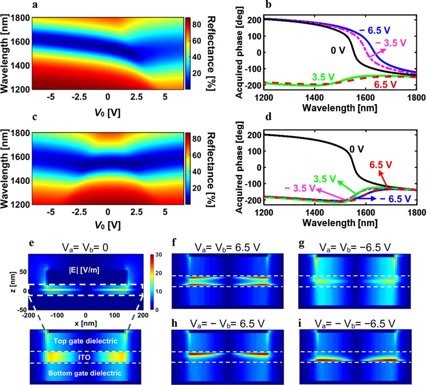
Nano Letters Letter
approach enables continuous tuning of the phase of emitted
light from 0 to 360° upon application of external bias. However,
the large pixel size of the phased array (9 μm × 9 μm) results in
undesired side lobes. Moreover, thermo-optic control limited
the modulation frequency of these phased arrays to less than 50
kHz,32 which is too slow for versatile beam steering in
technologically important LIDAR applications, and the thermal
crosstalk between phase shifters and the photodetectors limited
the detection range to 20°.33
Metasurfaces offer a different approach to a phased array
architecture, in which the array is intrinsically two-dimensional
and the subwavelength antenna dimensions and antenna
spacing can suppress side lobes. Hence, it would be highly
desirable to have a tunable metasurface platform for
comprehensive and active control of scattered light in the
near-infrared spectral range. We have previously investigated
field-effect modulation of the carrier density and refractive
index of heavily doped semiconductors as an approach to
actively tunable near-infrared metasurfaces.34 This approach
relies on the field effect-induced charge accumulation or
depletion in the semiconducting electrode of a nanoscale
metal−oxide−semiconductor (MOS) structure that also serves
as a resonant antenna. Using ITO as a semiconducting layer of
the MOS field effect structure enabled active modulation of the
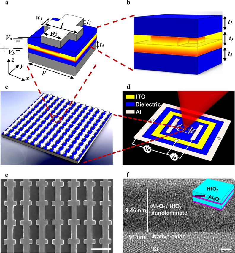
optical response of plasmonic reflectarray metasurfaces34,35 Figure 1. (a) Schematic of the unit cell of the dual-gated metasurface,
with a corresponding reflected light phase shift from 0 to 184° which is composed of an Al back reflector, a bottom gate dielectric, an
for an applied bias between 0 to 2.5 V. Although conceptually ITO layer, followed by another gate dielectric on top of which Al
promising as an approach to active metasurface design, in order fishbone antennas are located. The thicknesses of the antenna array,
to realize a comprehensively tunable metasurface a phase shift the gate dielectrics, the ITO layer, and the back reflector are t1= 40
from 0° approaching to 360° is desirable. nm, t2= 9.5 nm, t3= 5 nm, and t4= 80 nm, respectively. The antenna
dimensions are l = 280 nm and w1 = 120 nm, and the electrode width
We report here the design and fabrication of dual-gated field-
is w2 = 170 nm. The period of the metasurface is p = 400 nm. A
effect-tunable metasurface antenna arrays that enable phase voltage bias Va is applied between the ITO layer and the top antennas,
shifts exceeding 300° at a wavelength of λ = 1550 nm. Our while another voltage bias Vb is applied between the Al back reflector
dual-gated metasurface features two charge accumulation/ and the ITO layer. The two applied voltage biases result in the
depletion layers within the dielectric spacer of each active formation of two accumulation/depletion regions in the ITO layer at
metasurface antenna (Figure 1a). The dual-gated metasurface the top and bottom ITO/gate-dielectric interfaces. (b) A magnified
structure consists of an Al back reflector, a gate-dielectric/ITO/ image of the dielectric spacer of the metasurface that consists of the
gate-dielectric heterostructure and a periodic array of Al top gate dielectric, the ITO layer, and the bottom gate dielectric. (c)
nanoantennas with a “fishbone” pattern (Figures 1a, b). A Schematic of the metasurface. (d) Schematic showing the bias
scanning electron microscope (SEM) image of the antenna application configuration. The nanoantenna array is electrically
connected to an external pad to which we apply the voltage. (e)
array is shown in Figure 1c. Each metasurface element permits Scanning electron microscope image of our metasurface. Scale bar is
application of two independent dc voltages, (i) between the 500 nm. (f) Transmission electron microscope image of an Al2O3/
ITO layer and the fishbone antenna and (ii) between the ITO HfO2 nanolaminate, which serves as a gate dielectric in our
layer and the back reflector. As a result, both the top and metasurface. Scale bar is 2 nm. The Al2O3/HfO2 nanolaminate is
bottom ITO/gate-dielectric interfaces can exhibit the charge grown via atomic layer deposition (ALD). Our ALD process consists
accumulation or depletion under applied external bias. This of two growth periods each including 10 cycles of Al2O3 and 30 cycles
design facilitates a large variation of the complex refractive of HfO2, followed by a 30 s long rapid temperature annealing
index of the ITO layer via carrier density modulation at both its treatment at 600 °C. The inset shows the deposition sequence of the
top and bottom interfaces (Figure 1b) and is a key reason for nanolaminate.
the wide phase tunability of our dual-gated metasurface.
In designing dual-gated metasurfaces, we account for a
number of considerations that can increase the metasurface accumulation layer is strongly enhanced, resulting in the
tunability and efficiency. We choose the ITO carrier modulation of the intensity and phase of the scattered
concentration to be N0 = 3 × 1020 cm−3 to ensure that the light.15,36−38 The optical electric field enhancement in the
real part of the dielectric permittivity of the ITO layer is ENZ region of ITO arises from the continuity of the normal
positive at a wavelength of λ = 1550 nm when no external bias component of the electric displacement as the index approaches
is applied. Under bias, a charge accumulation layer is formed in zero in this region.36,37 This suggests that increasing the
the ITO, and the real part of the dielectric permittivity of the number of the accumulation/depletion layers within the active
accumulation layer can change its sign, undergoing the region of the metasurface antenna is beneficial for enhancing
transition from the optically dielectric to optically metallic phase tunability. On the other hand, since the optical loss of the
phase. When the dielectric permittivity of the accumulation ITO layer is non-negligible (Supporting Information Part 1),
layer is in the epsilon-near-zero (ENZ) region, which means −1 we design the ITO layer to be as thin as possible to ensure
< Re(ε) < 1, the optical electric field intensity in the higher reflectance. On the basis of these considerations, the
2958 DOI: 10.1021/acs.nanolett.8b00351
Nano Lett. 2018, 18, 2957−2963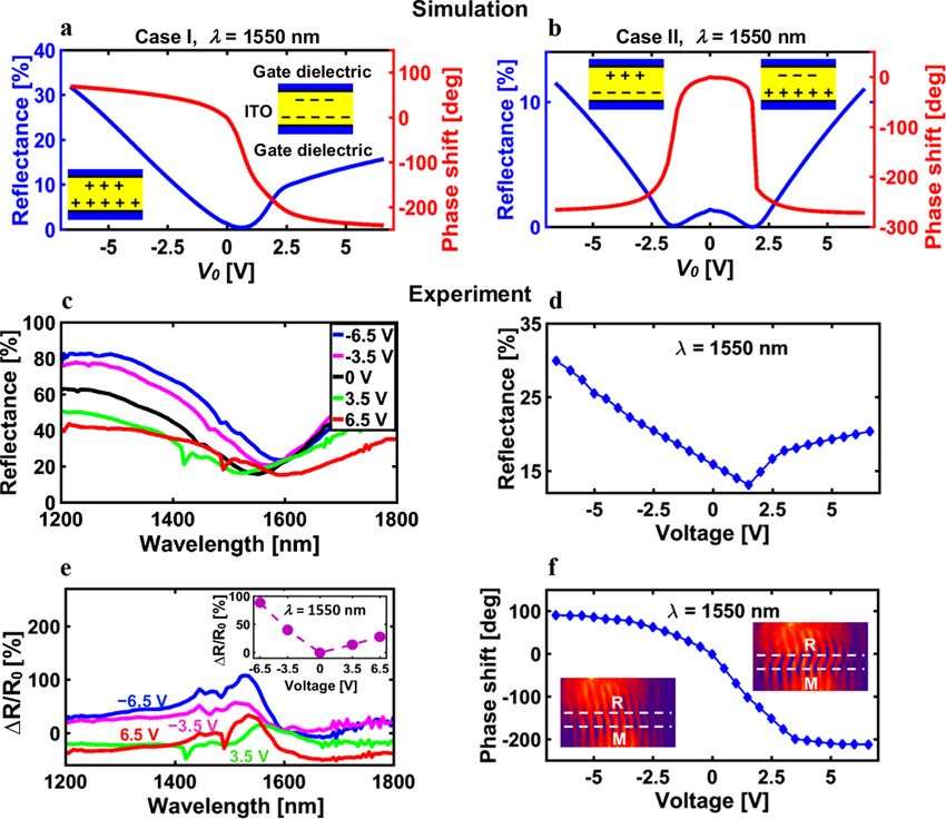
Nano Letters                                                                                                                                Letter

ITO layer thickness is chosen to be 5 nm in our dual-gated                   nanolaminate via ALD, and sputtered a 5 nm-thick layer of
metasurface.                                                                 ITO. We chose the ITO carrier concentration to be N0 = 3 ×
   Another parameter that determines the performance is the                  1020 cm−3. To characterize our ITO films, we performed Hall
choice of the plasmonic metal. The work functions of Al and                  measurements and spectroscopic ellipsometry on 5 nm-thick
Ag, which are both near 4.3 eV, are quite close to the work                  ITO layers deposited on quartz and Si substrates, respectively.
function of ITO when the carrier concentration equals N0 = 3                 Once we deposited the ITO layer, we deposited the top gate
× 1020 cm−3, while the work function of Au (5.1 eV) is                       dielectric, consisting of a 9.5 nm-thick HAOL layer. Finally, we
significantly higher than that of the ITO. Hence, using Al or Ag              fabricated a 40 nm-thick Al fishbone antenna array on top of
as a metal electrode in the metal/gate-dielectric/ITO capacitor              the upper HAOL layer by electron beam evaporation of Al and
reduces the zero-bias band bending in the ITO layer compared                 patterning by electron beam lithography. The antenna width
to an Au electrode. This implies that in the case of Al or Ag                and length were w1= 120 nm and l = 280 nm, and the width of
electrodes, one needs to apply lower bias voltages to overcome               the stripe electrode was w2= 170 nm (Figure 1a). During
the depletion and form an accumulation layer in the ITO at the               fabrication, our samples were patterned to allow for easy
gate-dielectric/ITO interface. Previous research has indicated               application of a bias between the Al back reflector and the ITO
that Ag can also migrate into the gate dielectric layers under               layer (Vb in Figure 1d). The Al fishbone antennas were
applied electrical bias.26,39 To eliminate this issue, we use Al, a          connected to an external Al pad that allows for facile bias
CMOS-compatible material, as the plasmonic metal in our                      application between the fishbone antennas and the ITO layer
tunable metasurfaces.                                                        (Va Figure 1d). The electrode pads were then wire bonded to a
   The attainable optical modulation in our tunable metasurface              compact chip carrier and circuit board for electrical gating.
is also determined by the choice of the gate dielectric material.            Figure 1d shows the bias configuration for dual-gated
To enable the largest possible variation of carrier density in               metasurfaces.
ITO under applied voltage, one would ideally like to have a gate                Electromagnetic Simulations of Dual-Gated Metasur-
dielectric with high dc permittivity and high breakdown field.                faces. We modeled the optical response of our metasurface
Al2O3 and HfO2 are among the most commonly used high                         under applied bias using finite difference time domain
dielectric constant gate dielectric materials, employed in field-             simulations coupled to device physics simulations. The device
effect transistor technology. Al2O3 exhibits good thermal                     physics simulations were used to determine the charge carrier
stability and almost perfect interfacial properties with Si-based            distribution in the ITO layer under applied bias. We then
substrates, has a large bandgap, and a high breakdown field of                related the calculated carrier density to the complex dielectric
up to 10 MV/cm.40,41 However, it suffers from a relatively low                permittivity of ITO εITO using a Drude model approach: εITO =
dc permittivity of kAl2O3 = 9. On the other hand, HfO2 is a                  ε∞ − ω2p/(ω2 + iωγ), because the plasma frequency ωp is
                                                                             proportional to the square root of the carrier density of ITO
CMOS compatible material with a wide bandgap, and relatively                 (NITO). Here, γ is the damping constant and ε∞ is a fitting
high dielectric constant of up to kHfO2 = 25. But it exhibits a              constant. ωp, γ, and ε∞ at zero bias are determined empirically
small breakdown field of 3.1 MV/cm, and high leakage current                  from Hall measurements and ellipsometry (Supporting
induced by its low crystallization temperature. Previous                     Information Part 3). ω is the angular frequency, which is
research has shown that Al2O3/HfO2 nanolaminates, com-                       related to the wavelength λ as λ=2πc/ω, where c is the speed of
monly referred to as “HAOL” materials, can have superior                     light in vacuum.
electrostatic characteristics as compared to both Al2O3 and                     The electrostatic performance of the dual-gated tunable
HfO2.42 HAOL structures, which are grown via consecutive                     metasurface element can be viewed as two parallel plate
deposition of ultrathin Al2O3 and HfO2 layers, have previously               capacitor structures which are connected in series. Therefore,
shown to have the low leakage current and high breakdown                     two independent bias voltages can be applied to each
field characteristics of Al2O3 and also the large dc permittivity             metasurface element, Va and Vb (Figure 1a). In what follows
characteristic of HfO2. During our fabrication process, we grew              we assume that |Va| = |Vb| that now yields two accessible
thin HAOL films by using atomic layer deposition (ALD) and                    regimes of device operation, where sign(Va × Vb) ≥ 0 (Case I)
compared their properties with separately grown Al2O3 and                    and where sign(Va × Vb) ≤ 0 (Case II). In other words, in Case
HfO2 films (for fabrication details see Supporting Information                I there is a simultaneous charge accumulation or simultaneous
Part 2). We used transmission electron microscopy (TEM), as                  charge depletion at both ITO layer interfaces (Figure 2a,c,e). In
well as capacitance−voltage (C−V) and current−voltage (I−V)                  Case II, charge accumulation at the top ITO/HAOL interface is
measurements to characterize the deposited films. We found                    accompanied by charge depletion at the bottom ITO/HAOL
that the dc permittivities of our Al2O3, HfO2, and HAOL films                 interface or, vice versa, charge depletion at the top ITO/HAOL
were equal to kAl2O3 = 10.5, kHfO2 = 17.8, and kHAOL = 22,                   interface is accompanied by charge accumulation at the bottom
respectively. Furthermore, the measured breakdown fields of                   ITO/HAOL interface (Figure 2b,d,f). The charge carrier
the fabricated Al2O3, HfO2, and HAOL films were EAl2O3 = 7.4                  distributions in the 5 nm-thick ITO layer for Case I and
                                                                             Case II are depicted in Figure 2c,d, respectively. Here, the z-
MV/cm, EHfO2 = 3.1 MV/cm, and EHAOL = 7.2 MV/cm,                             position varies between 0 and 5 nm with 0 corresponding to
respectively. Because HAOL structures showed superior                        the bottom ITO/HAOL interface and 5 nm corresponding to
electrostatic performance as compared to the Al2O3 and                       the top ITO/HAOL interface.
HfO2 films, we used HAOL structures as the gate dielectric                       We note that only the portion of the ITO located directly
in our dual-gated metasurfaces.                                              beneath the Al fishbone antenna is optically modulated at the
   After identifying the optimal constituent materials, we                   top ITO/HAOL interface (Figure 1b). As seen in Figure 2c, in
fabricated dual-gated tunable metasurfaces. First, we deposited              Case I the ITO dielectric permittivity at the bottom ITO/
an 80 nm-thick Al back reflector on a 100 Si wafer by electron                HAOL interface is always equal to the dielectric permittivity of
beam evaporation. Next, we grew a 9.5 nm-thick Al2O3/HfO2                    the ITO at the top ITO/HAOL interface beneath the fishbone
                                                                      2959                                            DOI: 10.1021/acs.nanolett.8b00351
                                                                                                                       Nano Lett. 2018, 18, 2957−2963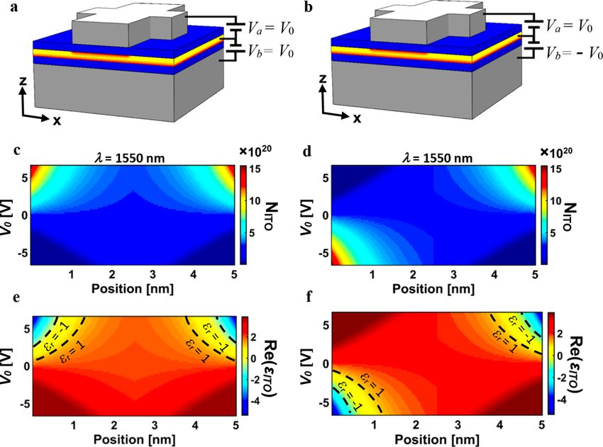
Nano Letters                                                                                                                                          Letter

Figure 2. (a) Schematic of Case I in which there is a simultaneous
charge accumulation or simultaneous charge depletion at both ITO/
HAOL interfaces of the ITO layer. In Case I, we assume Va = V0 and
Vb = V0. (b) Schematic of Case II in which the charge accumulation
(depletion) at the top ITO/HAOL interface is always accompanied by                 Figure 3. (a) Reflectance from the metasurface as a function of
the charge depletion (accumulation) at the bottom ITO/HAOL                         wavelength and applied voltage in Case I. (b) Phase spectrum of the
interface. In Case II, we assume Va = V0 and Vb = −V0. The charge                  reflected light for different applied voltages in Case I. (c) Reflectance
carrier distribution in the ITO layer as a function of applied voltage V0          as a function of wavelength and applied bias in Case II. (d) Phase
for (c) Case I and (d) Case II. The real part of the dielectric                    spectrum for different applied voltages in Case II. (e) Spatial
permittivity of the ITO layer as a function of the applied voltage and             distribution of the magnitude of the electric field inside the
position for (e) Case I and (f) Case II at a wavelength of λ = 1550 nm.            metasurface element at no applied bias. The bottom part of (e)
The boundaries of the ENZ regions are marked by dashed curves.                     shows the magnified image of the field distribution in the HAOL/
                                                                                   ITO/HAOL dielectric spacer of the metasurface. The close-up of the
                                                                                   distribution of the electric field magnitude in the dielectric spacer of
antenna. This, however, is not true for Case II. In Case II, for                   the metasurface when (f) V0 = 6.5 V in Case I, (g) V0 = −6.5 V in Case
sufficiently large applied voltage magnitude, there is always                        I, (h) V0 = 6.5 V in Case II, (i) V0 = −6.5 V in Case II.
charge accumulation at either top or bottom interface of the
ITO layer (Figure 2d).
   After modeling the complex dielectric permittivity of ITO as                    distribution of the optical electric field. Figure 3f shows the
a function of position and applied voltage, we calculated the                      optical electric field distribution in Case I at an applied voltage
metasurface optical response for different applied biases under                     of V0 = 6.5 V. As seen in Figure 3f, the optical electric field is
normal incidence illumination with a transverse magnetic (TM)                      enhanced at both the top and bottom ITO/HAOL interfaces
polarized plane wave (E-field along x-direction). Figure 3a                         due to the ENZ regions that are formed at these interfaces
shows the dual-gated metasurface reflectance in Case I as a                         (Figure 2e). On the other hand, when the applied dc bias in
function of wavelength and applied voltage. In this case, a large                  Case I is equal to V0 = −6.5 V, the ITO layer is depleted at
reflectance modulation and large phase shift (Figure 3b) are                        both top and bottom interfaces (Figure 2c−e) and therefore we
observed at positive biases, when the dielectric permittivity of                   do not observe a significant optical field enhancement in the
both the top and bottom ITO interfaces crosses into the ENZ                        ITO layer (Figure 3g). In Case II, however, a dramatic optical
region. The phase shift is defined as a difference between the                       field enhancement is observed at both positive and negative
phases of the reflected and incoming plane waves calculated at                      applied biases V0 = ±6.5 V (Figure 3h,i). In this case at an
the same spatial point. In Case I, we observe a blue shift of the                  applied bias of V0 = 6.5 V, we observe the optical electric field
resonance when the applied bias increases from 0 to 2.5 V. For                     enhancement in the ITO layer around the top ITO/HAOL
applied voltages larger than 2.5 V, the resonance redshifts. This                  interface due to the ENZ region formed in the ITO layer
is consistent with previously reported results.34 In Case II, we                   (Figure 3h). Similarly, Figure 3i shows that in Case II, the
observe a significant reflectance and phase modulation both at                       optical electric field is enhanced around the bottom part of the
positive and negative biases (Figure 3c,d). Moreover, we                           ITO layer, when the applied bias is equal to V0 = −6.5 V (for
observe that in Case II the reflectance spectrum is invariant                       further field profiles, see Supporting Information Part 4). The
with respect to the transformation V0 → −V0. This is because in                    analysis of the optical field profile suggests that strong light
Case II both at positive and negative biases the gap plasmon                       confinement in the dielectric gap of the plasmonic antenna
resonance couples to the ENZ region in ITO that is formed in                       significantly contributes to the observed optical modulation.
either the top or the bottom ITO layer interface.                                     Figure 3b,d illustrates how dual-gated metasurfaces signifi-
   To gain further insight, we plotted the distribution of the                     cantly alter the phase of the reflected light under an applied
absolute value of the optical electric field in the metasurface                     bias. In Figure 4, we plot the phase shift and reflectance as a
element for the resonant wavelength of λ = 1550 nm (Figure                         function of applied bias V0 at a wavelength of λ = 1550 nm.
3e−i). Figure 3e shows the spatial distribution of the optical                     Figure 4a, which corresponds to Case I, shows that this bias
electric field at zero bias. The bottom part of Figure 3e shows                     configuration gives a continuously tunable phase shift between
the magnified region of the dielectric spacer at zero bias. When                    70° and −245°, when the applied voltage is varied between V0
a dc bias is applied, we observe a significant variation of the                     = −6.5 V and V0 = 6.5 V. This amounts to a total tunable phase
                                                                            2960                                                DOI: 10.1021/acs.nanolett.8b00351
                                                                                                                                 Nano Lett. 2018, 18, 2957−2963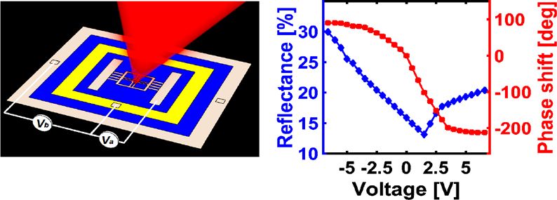
Nano Letters                                                                                                                                     Letter

                                                                                 3a), which indicate that at an applied voltage of V0 = 2.5 V we
                                                                                 reach the ENZ region in the ITO accumulation layer,
                                                                                 corresponding to the transition from resonance blue shift to
                                                                                 red shift.
                                                                                    Figure 4d displays the reflectance as a function of applied
                                                                                 voltage V0 at a wavelength of λ = 1550 nm. We observe a
                                                                                 decrease in reflectance when the applied voltage increases from
                                                                                 V0 = −6.5 V to V0 = 0.6 V. Once the applied bias has passed V0
                                                                                 = 0.6 V, we observe an increase in reflectance (Figure 4d).
                                                                                 Figure 4e shows relative reflectance spectra ΔR/R0 = [R(V0) −
                                                                                 R(0)]/R(0) at different applied voltage values V0. Even though
                                                                                 the measured reflectance modulation ΔR/R0 is fairly broad-
                                                                                 band, we observe an enhancement in ΔR/R0 around the
                                                                                 metasurface resonant wavelength. The inset of Figure 4e shows
                                                                                 the relative reflectance modulation ΔR/R0 as a function of
                                                                                 applied bias V0 at a wavelength of λ = 1550 nm. At a
                                                                                 wavelength of λ = 1550 nm, the relative reflectance modulation
                                                                                 is much more significant for negative rather than positive bias
                                                                                 voltages. When V0 decreases from V0 = 0 V to V0 = −6.5 V, we
                                                                                 observe a relative reflectance modulation of 89% at a
Figure 4. (a,b) Simulated reflectance and phase shift of the                      wavelength of λ = 1550 nm. On the other hand, when applied
metasurface as a function of voltage V0. The wavelength is fixed at λ
                                                                                 voltage V0 increases from V0 = 0 V to V0 = 6.5 V, the observe
= 1550 nm. The panel (a) corresponds to Case I, in which there is a
simultaneous charge accumulation or simultaneous charge depletion in             that the relative reflectance modulation is only 28% (see the
the ITO layer at the both ITO/HAOL interfaces. The panel (b)                     inset of Figure 4e). This implies that at the resonance
corresponds to Case II in which the charge accumulation at the top               wavelength, the formation of multiple ITO charge depletion
ITO/HAOL interface is always accompanied by the charge depletion                 layers influences the reflectance more significantly than the
at the bottom ITO/HAOL interface and vice versa. The insets of (a,b)             formation of multiple charge accumulation layers. This change
schematically show the charge distribution in the dielectric spacer of           in reflectance can be explained by the modulation of the optical
the metasurface. (c) Measured reflectance spectra in Case I at different           electric field in the ITO layer under applied bias. At V0 = 0 V,
applied voltages V0. (d) Measured reflectance in Case I as a function of          the formation of the magnetic dipole leads to strong absorption
applied bias V0 and at the fixed wavelength of λ = 1550 nm. (e) The               in the ITO layer, whereas the applied bias effectively modulates
spectra of the relative reflectance modulation ΔR/R0 for different
applied voltages V0. The inset shows the relative reflectance change at
                                                                                 the optical field distribution in the dielectric spacer of the
a wavelength of λ = 1550 nm as a function of applied bias V0. (f)                metasurface and leads to higher reflectance.
Measured phase shift of the metasurface as a function of applied                    After performing metasurface gate-tunable reflectance
voltage V0 at a wavelength of λ = 1550 nm. The insets of (f) show the            measurements and identifying the resonance wavelength, we
interference fringes at −6.5 V and +6.5 V. The dashed lines labeled as           measured the phase shift of the reflected light under applied
R and M indicate the interference fringes from the reference and                 bias. For our phase shift measurements, we employed a
metasurface, respectively.                                                       Michelson interferometer-type (Supporting Information Part
                                                                                 7). In our interferometer, laser light illuminated the edge of the
shift of 315° derived from Case I. As expected, a phase shift                    metasurface. Therefore, a part of the incoming beam was
derived from Case II is invariant with respect to the                            reflected from the metasurface, while the other part was
transformation V0 → −V0 (Figure 4b). In Case II, the phase                       reflected from the surrounding planar Al/HAOL/ITO/HAOL
shift smoothly varies between 0 and −275°, when the applied                      heterostructure, which acted as a built-in phase reference. The
voltage is increased from V0 = 0 V to V0 = 6.5 V. Thus, via an                   images of the formed interference fringes were recorded by a
appropriate bias application, the proposed dual-gated tunable                    charge-coupled device camera and subsequently were processed
metasurface allows us to attain a tunable phase shift of 345°.                   and fitted. Our fitting procedure enabled us to retrieve the
    Experimental Results. Having identified an approach to                        relative displacement of the interference fringes originating
metasurface design, we fabricated and characterized the tunable                  from the metasurface and the reference when we applied a bias.
optical response of dual-gated metasurfaces (for fabrication                        The measured interference fringe displacement was con-
details and measurement setups see Supporting Information                        verted into a relative phase shift (Supporting Information Part
Parts 5−7). Optical measurements were performed by                               7). Our interferometry enabled accurate phase measurements,
illuminating our metasurfaces with linearly polarized light                      because in this configuration errors caused by vibrations and
with incident electric field aligned with the fishbone antenna (x-                 other motion instabilities were eliminated. Examples of
direction in Figure 1a). In our experiments, the bias                            interference fringe images recorded at bias voltages of V0 =
configuration corresponds to Case I, when Va = V0 and Vb =                        −6.5 V and V0 = +6.5 V are shown in the inset of Figure 4f. In
V0 (Figure 2a). Figure 4c displays the measured reflectance                       this measurement, the laser illumination wavelength is λ = 1550
spectra at different values of applied voltage V0. The resonance                  nm. The dashed white lines show the interference fringes from
is observed to blue shift with increasing voltage from V0 = 0 V                  the metasurface (M) and the reference (R). Figure 4f shows the
to V0 = 2.5 V. When we increased the applied voltage from V0 =                   measured phase shift as a function of applied voltage V0 (λ =
2.5 V to V0 = 6.5 V, the resonance was observed to red shift,                    1550 nm). When we increased the applied voltage from V0 = 0
and likewise when we decreased the applied bias from V0 = 0 V                    V to V0 = +6.5 V, we observed a phase shift of −211.9°, which
to V0 = −6.5 V, a resonance red shift was observed. These                        is accompanied by a modest relative reflectance modulation of
observations are consistent with our simulation results (Figure                  28%. When we decreased the applied voltage from V0 = 0 V to
                                                                          2961                                             DOI: 10.1021/acs.nanolett.8b00351
                                                                                                                            Nano Lett. 2018, 18, 2957−2963
Nano Letters Letter
V0 = −6.5 V, we measured a phase shift of +91° that is
consistent with our simulation results shown in Figure 4a.
■ REFERENCES
(1) Yu, N.; Genevet, P.; Kats, M. A.; Aieta, F.; Tetienne, J.-P.;
Interestingly, despite the modest phase shift recorded at Capasso, F.; Gaburro, Z. Science 2011, 334, 333−337.
negative biases V0 < 0, the reflectance measured at a wavelength (2) Yu, N.; Capasso, F. Nat. Mater. 2014, 13, 139−150.
λ = 1550 nm increases from 13% to 30%. An overall phase shift (3) Arbabi, A.; Horie, Y.; Bagheri, M.; Faraon, A. Nat. Nanotechnol.
of 303° was produced as the applied bias to the dual-gated 2015, 10, 937−943.
metasurface was varied between V0 = −6.5 V and V0 = +6.5 V. (4) Pors, A.; Nielsen, M. G.; Eriksen, R. L.; Bozhevolnyi, S. I. Nano
In summary, we have designed and fabricated a dual-gated Lett. 2013, 13, 829−834.
plasmonic reflectarray metasurface that shows wide phase (5) Khorasaninejad, M.; Chen, W. T.; Devlin, R. C.; Oh, J.; Zhu, A.
tunability with applied bias at a wavelength of λ = 1550 nm, and Y.; Capasso, F. Science 2016, 352, 1190−1194.
the phase of the reflected light can be continuously tuned from (6) Huang, Y.-W.; Chen, W. T.; Tsai, W.-Y.; Wu, P. C.; Wang, C.-M.;
Sun, G.; Tsai, D. P. Nano Lett. 2015, 15, 3122−3127.
0 to 303°. We have also measured a relative reflectance
(7) Zheng, G.; Muhlenbernd, H.; Kenney, M.; Li, G.; Zentgraf, T.;
modulation of 89%. This large optical tunability is achieved Zhang, S. Nat. Nanotechnol. 2015, 10, 308−312.
both due to the materials employed here and to the dual-gated (8) Chen, W. T.; Yang, K.-Y.; Wang, C.-M.; Huang, Y.-W.; Sun, G.;
metasurface architecture. Each element of our dual-gated Chiang, I.-D.; Liao, C. Y.; Hsu, W.-L.; Lin, H. T.; Sun, S.; et al. Nano
metasurfaces can be viewed as two series-connected MOS Lett. 2014, 14, 225−230.
field effect structures to which two independent bias voltages (9) Black, L.-J.; Wang, Y.; de Groot, C. H.; Arbouet, A.; Muskens, O.
can be applied, yielding a wider phase tuning range compared L. ACS Nano 2014, 8, 6390−6399.
to a single-gated metasurface (Supporting Information Part 8). (10) Wu, P. C.; Tsai, W.-Y.; Chen, W. T.; Huang, Y.-W.; Chen, T.-Y.;
Interestingly, in our case a given phase shift can be achieved via Chen, J.-W.; Liao, C. Y.; Chu, C. H.; Sun, G.; Tsai, D. P. Nano Lett.
multiple different bias configurations that yield different 2017, 17, 445−452.
reflectance values, enabling an approach for reflectance (11) Sherrott, M. C.; Hon, P. W. C.; Fountaine, K. T.; Garcia, J. C.;
modulation at a constant phase. This feature may be very Ponti, S. M.; Brar, V. W.; Sweatlock, L. A.; Atwater, H. A. Nano Lett.
useful for design and demonstration of future dynamically 2017, 17, 3027−3034.
(12) Dabidian, N.; Kholmanov, I.; Khanikaev, A. B.; Tatar, K.;
reconfigurable low-profile optical components such as focusing Trendafilov, S.; Mousavi, S. H.; Magnuson, C.; Ruoff, R. S.; Shvets, G.
lenses with reconfigurable focal lengths, dynamic holograms, ACS Photonics 2015, 2, 216−227.
and beam steering devices.
■
(13) Yao, Y.; Kats, M. A.; Genevet, P.; Yu, N.; Song, Y.; Kong, J.;
Capasso, F. Nano Lett. 2013, 13, 1257−1264.
ASSOCIATED CONTENT (14) Jun, Y. C.; Reno, J.; Ribaudo, T.; Shaner, E.; Greffet, J.-J.;
*
S Supporting Information Vassant, S.; Marquier, F.; Sinclair, M.; Brener, I. Nano Lett. 2013, 13,
The Supporting Information is available free of charge on the 5391−5396.
ACS Publications website at DOI: 10.1021/acs.nano- (15) Park, J.; Kang, J.-H.; Liu, X.; Brongersma, M. L. Sci. Rep. 2015, 5,
lett.8b00351. 15754.
(16) Lewi, T.; Evans, H. A.; Butakov, N. A.; Schuller, J. A. Nano Lett.
Additional information, tables, and figures (PDF) 2017, 17, 3940−3945.
■
(17) Iyer, P. P.; Pendharkar, M.; Palmstrom, C. J.; Schuller, J. A. Nat.
AUTHOR INFORMATION Commun. 2017, 8, 472.
(18) Cencillo-Abad, P.; Ou, J.-Y.; Plum, E.; Valente, J.; Zheludev, N.
Corresponding Author I. Nanotechnology 2016, 27, 485206.
*E-mail: haa@caltech.edu. (19) Ou, J.-Y.; Plum, E.; Zhang, J.; Zheludev, N. I. Nat. Nanotechnol.
ORCID 2013, 8, 252−255.
Ghazaleh Kafaie Shirmanesh: 0000-0003-1666-3215 (20) Valente, J.; Ou, J.-Y.; Plum, E.; Youngs, I. J.; Zheludev, N. I. Nat.
Ruzan Sokhoyan: 0000-0003-4599-6350 Commun. 2015, 6, 7021.
(21) Zhu, Z. H.; Evans, P. G.; Haglund, R. F.; Valentine, J. G. Nano
Harry A. Atwater: 0000-0001-9435-0201 Lett. 2017, 17, 4881−4885.
Present Address (22) Decker, M.; Kremers, C.; Minovich, A.; Staude, I.;
§
(R.A.P.) Metamaterial Technologies Inc. 5880 W. Las Positas Miroshnichenko, A. E.; Chigrin, D.; Neshev, D. N.; Jagadish, C.;
Blvd, Ste 51, Pleasanton, CA 94588, United States. Kivshar, Y. S. Opt. Express 2013, 21, 8879−8885.
(23) Sautter, J.; Staude, I.; Decker, M.; Rusak, E.; Neshev, D. N.;
Notes
Brener, I.; Kivshar, Y. S. ACS Nano 2015, 9, 4308−4315.
The authors declare no competing financial interest.
■
(24) Olivieri, A.; Chen, C.; Hassan, S.; Lisicka-Skrzek, E.; Tait, R. N.;
Berini, P. Nano Lett. 2015, 15, 2304−2311.
ACKNOWLEDGMENTS (25) de Galarreta, C. R.; Alexeev, A. M.; Au, Y.-Y.; Lopez-Garcia, M.;
This work was supported by Samsung Electronics (G.K.S., R.S., Klemm, M.; Cryan, M.; Bertolotti, J.; Wright, C. D. Adv. Funct. Mater.
and H.A.A.) and the Air Force Office of Scientific Research 2018, 28, 1704993.
under Grant FA9550-16-1-0019 (R.A.P.). The authors used (26) Thyagarajan, K.; Sokhoyan, R.; Zornberg, L.; Atwater, H. A. Adv.
facilities supported by the Kavli Nanoscience Institute (KNI) Mater. 2017, 29, 1701044.
and Joint Center for Artificial Photosynthesis (JCAP) at (27) Wu, P. C.; Papasimakis, N.; Tsai, D. P. Phys. Rev. Appl. 2016, 6,
044019.
Caltech. The authors would like to thank Carol Garland for
(28) Chu, C. H.; Tseng, M. L.; Chen, J.; Wu, P. C.; Chen, Y.-H.;
help with the TEM imaging. The authors gratefully acknowl- Wang, H.-C.; Chen, T.-Y.; Hsieh, W. T.; Wu, H. J.; Sun, G.; Tsai, D. P.
edge useful discussions with Dr. Yao-Wei Huang, Dr. Pin Chieh Laser Photonics Rev. 2016, 10, 1063−1063.
Wu, and Dr. Duhyun Lee. The authors also gratefully (29) Ee, H.-S.; Agarwal, R. Nano Lett. 2016, 16, 2818−2823.
acknowledge Erin Burkett and Christina Burch from the (30) Heck, M. J. R. Nanophotonics 2017, 6, 93−107.
Hixon Writing Center at Caltech for providing feedback and (31) Sun, J.; Timurdogan, E.; Yaacobi, A.; Hosseini, E. S.; Watts, M.
guidance on writing the manuscript. R. Nature 2013, 493, 195−199.
2962 DOI: 10.1021/acs.nanolett.8b00351
Nano Lett. 2018, 18, 2957−2963Nano Letters Letter
(32) Yaacobi, A.; Sun, J.; Moresco, M.; Leake, G.; Coolbaugh, D.;
Watts, M. R. Opt. Lett. 2014, 39, 4575−4578.
(33) Poulton, C. V.; Yaacobi, A.; Cole, D. B.; Byrd, M. J.; Raval, M.;
Vermeulen, D.; Watts, M. R. Opt. Lett. 2017, 42, 4091−4094.
(34) Huang, Y.-W.; Lee, H. W. H.; Sokhoyan, R.; Pala, R. A.;
Thyagarajan, K.; Han, S.; Tsai, D. P.; Atwater, H. A. Nano Lett. 2016,
16, 5319−5325.
(35) Park, J.; Kang, J.-H.; Kim, S. J.; Liu, X.; Brongersma, M. L. Nano
Lett. 2017, 17, 407−413.
(36) Lee, H. W.; Papadakis, G.; Burgos, S. P.; Chander, K.; Kriesch,
A.; Pala, R.; Peschel, U.; Atwater, H. A. Nano Lett. 2014, 14, 6463−
6468.
(37) Vasudev, A. P.; Kang, J.-H.; Park, J.; Liu, X.; Brongersma, M. L.
Opt. Express 2013, 21, 26387−26397.
(38) Lu, Z.; Zhao, W.; Shi, K. IEEE Photonics J. 2012, 4, 735−740.
(39) Lee, J.; Lu, W. D. Adv. Mater. 2018, 30, 1702770.
(40) Ye, P. D.; Yang, B.; Ng, K. K.; Bude, J.; Wilk, G. D.; Halder, S.;
Hwang, J. C. M. Appl. Phys. Lett. 2005, 86, 063501.
(41) Hinkle, C. L.; Sonnet, A. M.; Vogel, E. M.; McDonnell, S. Appl.
Phys. Lett. 2008, 92, 071901.
(42) Cao, D.; Cheng, X.; Zheng, L.; Xu, D.; Wang, Z.; Xia, C.; Shen,
L.; Yu, Y.; Shen, D. J. Vac. Sci. Technol., B: Nanotechnol. Microelectron.:
Mater., Process., Meas., Phenom. 2015, 33, 01A101.
2963 DOI: 10.1021/acs.nanolett.8b00351
Nano Lett. 2018, 18, 2957−2963You can also read