Silicon, ASICs, and Other Detectors - Eric Wulf Naval Research Laboratory
←
→
Page content transcription
If your browser does not render page correctly, please read the page content below

Silicon, ASICs, and Other Detectors

                 Eric Wulf
         Naval Research Laboratory
Silicon for Compton
Low-Z
Great Compton scatterer
Smallest Doppler broadening of materials under discussion
Need many layers to get interaction probability
All Silicon instrument does not make sense
Too effective at scattering
Too many chances to interact in passive material
Full absorption unlikely
Need High-Z material for full absorption of incident gamma-ray
while maintaining energy resolution
Ge, CZT, CdTe
Thin vs Thick Silicon
Thin
Pros
Electron tracking
Position resolution
Cons
Number of electronics channels
Number of layers
Thick
Pros
Fewer detectors and electronics
Increased interaction probability per layer
Cons
No electron tracking
Currently no depth resolution
Current Thick Silicon Detectors
150 mm diameter wafers
2 mm thick BNL ASIC FPGA & USB
Strip pitch of 1.41 mm
64 strips
Depletion voltage of ~700V
Leakage current of 300-700 nA at
room temperature
270 nA in dry nitrogen
4 nA/strip ignoring guard ring
~100 nA at 4° C
6” Detector
ASIC Design
Si Strip Detector ASIC
[De Geronimo, et al. 2008]
• 32 channels – pos/neg polarity § Front-end power, Detector Capacitance, Peaking
• 200 e- RMS at 30 pF and 4 us
peaking Time and Noise/Resolution are related and
• 400:1 dynamic range influence ASIC design
• Peak Detect and memory
• Readout mux § Threshold of the system is dependent on the
• 5 mW per channel resolution
Timing Energy Threshold ~ (ENC)(Peaking Time)/(Timing Resolution)
25 keV threshold for 1 us peaking and 10 ns time resolution
5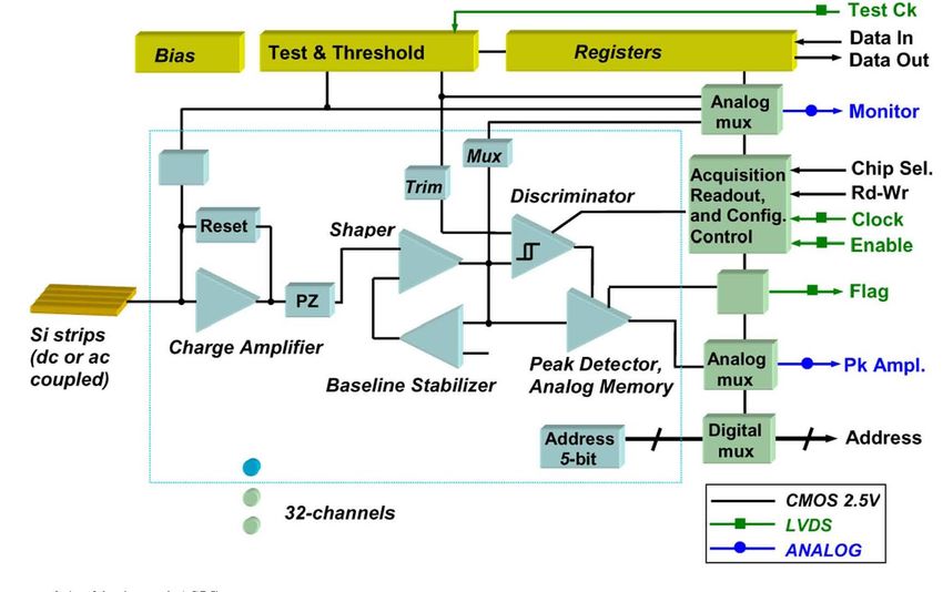
ASIC Readout
Developed at BNL Spectrum of a 133Ba source
with ~4 keV FWHM resolution
32 channels per ASIC
Polarity selection
Preamp, shaper, leading-edge
discriminator, peak & hold, sparsification
4 peaking times (0.5, 1, 2, 4 µs) Small detector cooled to -40C with
1.4 keV FWHM at 59.5 keV
15 keV – 3.7 MeV energy range
Dual gain settings Am-241
4 mW/channel – 166 mW/ASIC Co-57
81.5 cm2 x 0.2 cm with 4 ASICs
~0.5 gm/cm2
Full detector at room temperature
123 cm2/W or 57 g/W with 4.8 keV FWHM at 59.5 keV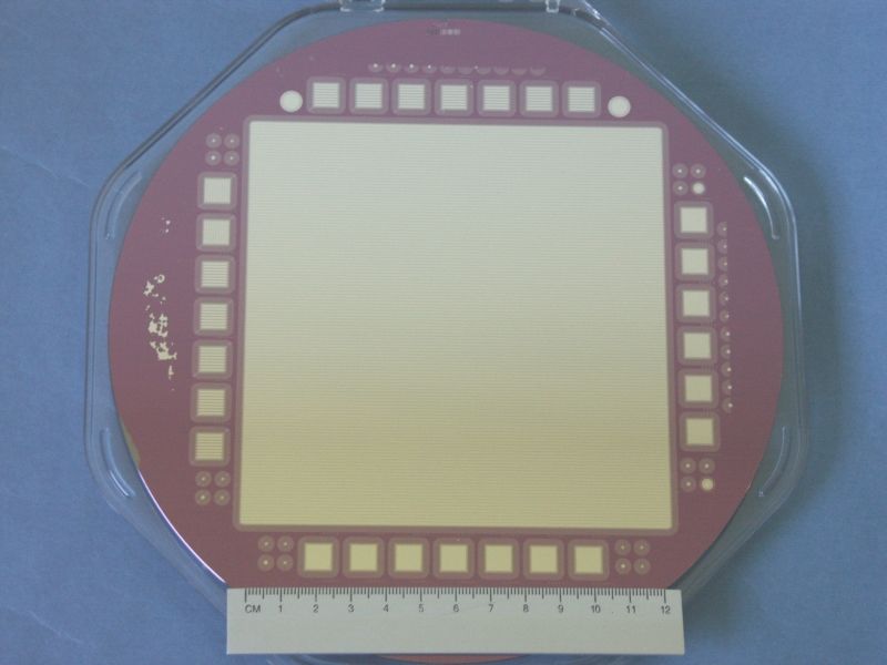
Silicon & CZT Compton Telescope
CZT detector available from
collaboration with Washington
University
Pixelization
0.25 mm
ASIC readout with BNL ASIC
Silicon scatterer and CZT
calorimeter
Integrated into one box
Logic levels connected
Coincident pulser data
Coincident gamma-ray data
Reconstructed data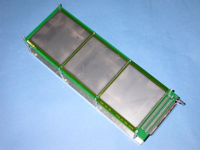
CZT Results

                  25 cm

                Source

Silicon
          CZT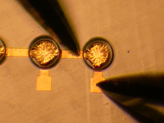
Large Area Detectors
Made at NRL
200 mm diameter wafer
675 µm thick
Thickest material currently available
156 cm2 active area
128 strips
920 µm wide and 124 mm long
Guard ring structure 2.3 mm wide
9 kΩ-cm
Depletion at ~60 V
Leakage current of 100 nA
6 keV FWHM at 59.5 keV
10% usable strips
Small detector at edge
2.6 keV FWHM at 59.5 keV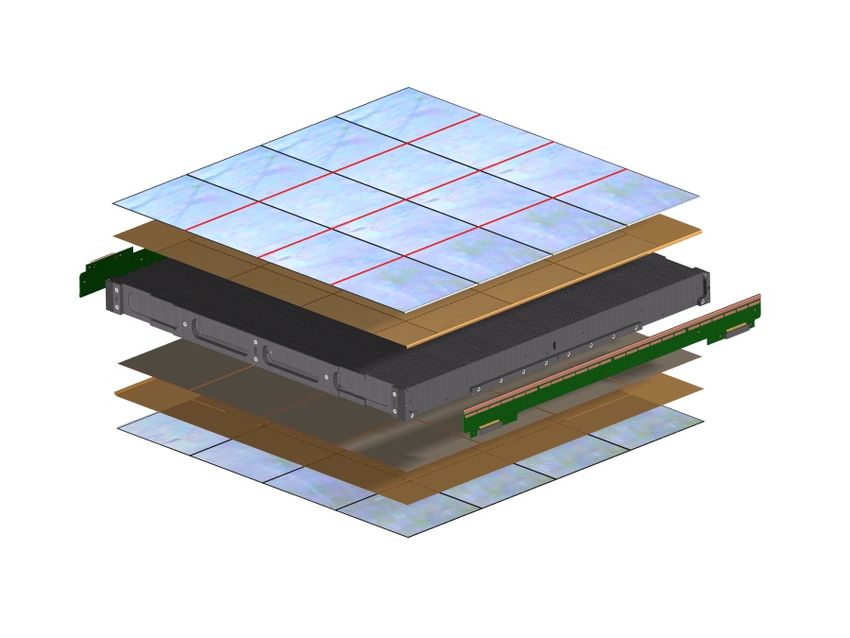
Daisy Chaining Detectors
LAT Tracker Tray Silicon Compton Tray
4x4 array Single sided SSD 3x3 array Double sided SSD
Front End Electronics
Front End Electronics
4x4 array Single sided SSD
Silicon Compton requires double-sided strip Requires spectroscopy of events in
detectors to position the Compton silicon
interactions in a single crystal more complex front ends
Preferred detector thickness is 2 mm or Pulse amplitude measurement
greater Performance improves with lower energy
Higher depletion voltages threshold – better noise performance
Higher quality silicon material Fewer channels but likely higher power
per channel
10Tiling Detectors
Reduce electronics needed
Move electronics to
perimeter
Decreased passive mass 3 9-cm detectors in series
64 strips (1.4 mm pitch).
Connect detectors in
ladder
3x3 array reduces number
of ASICs from 36 to 12
Increased capacitance (~ 30
pF per strip)
368 cm2/W or 73.6 g/W 133Ba line (356 keV) for 1 (black: 5.2
keV), 2 (red: 6.8 keV) and 3 (blue:
New version of the ASIC can 7.6 keV) detectors coupled together.
further reduce powerFuture of Silicon
Extensive research effort ongoing in Silicon
Many groups pursuing silicon detectors
For a Compton telescope
Improve energy resolution at room temperature
Increase area of the detectors
Increase thickness of the detectors
Improved ASICs with decreased power requirements
3x3 array of 5 mm thick 6” detectors
734 cm2 x 0.5 cm using 12 ASICs
184 g/WPrototype Concept
3x3 array of thick silicon
detectors
Surrounded by high-Z detectors
(Ge, CZT, CdTe) to absorb
scattered gamma-raysCdTe Reusable Interconnects
metal contact
elastomeric
material
(“rubber-like”
material
made from
silicone)
sensor (pixel
array)
flexible
silicone bump
read-out
ASICCurrent Semiconductor Detectors
Detector Pros Cons
Thick Silicon Fewer electronics channels, Low- Suitable primarily as scatterer, Best
Doppler Broadening, good energy resolution at < 0° C, 0.5 – 1 cm
resolution thick is optimal
Thin Silicon Electron tracking, Low-Doppler Suitable primarily as scatterer,
Broadening, good energy Increased number of electronics
resolution channels, Small g/cm2
CZT Very large g/cm2, True room Individual detectors fairly small,
temperature operation Large Doppler-broadening when used
as scatterer
CdTe Large crystals, Readout Currently only 1 mm thick, Large
properties similar to Silicon and Doppler-broadening when used as
Germanium scatterer
Germanium Best energy resolution, Signal Higher Doppler-broadening if used as
processing allows 3D tracking scatterer, Cooling/Large power
demandsLow Signal Sensing
Reduce counts by a factor of 5
164 events
No discernable Cs-137 peak
No discernable localization
Cut on the isotope energy
12 events
Localization apparent
7 (almost 8) go through correct
positionThick Silicon Goal
Push for largest area detectors
Reduce passive mass
Reduce electronics count
Push for thickest detectors
Reduce passive mass
Reduce electronics count
Increase interaction probability per layer
Final Goal
12” wafers with 5 mm thick silicon
1.2 g/cm2
156 cm2 active area
Elements being approached by B. Phlips and M. ChristophersenYou can also read