Light Trapping in Silicon Nanowire Solar Cells
←
→
Page content transcription
If your browser does not render page correctly, please read the page content below
pubs.acs.org/NanoLett

Light Trapping in Silicon Nanowire Solar Cells
Erik Garnett and Peidong Yang*
Department of Chemistry, University of California, Berkeley, California 94720

   ABSTRACT Thin-film structures can reduce the cost of solar power by using inexpensive substrates and a lower quantity and quality
   of semiconductor material. However, the resulting short optical path length and minority carrier diffusion length necessitates either
   a high absorption coefficient or excellent light trapping. Semiconducting nanowire arrays have already been shown to have low
   reflective losses compared to planar semiconductors, but their light-trapping properties have not been measured. Using optical
   transmission and photocurrent measurements on thin silicon films, we demonstrate that ordered arrays of silicon nanowires increase
   the path length of incident solar radiation by up to a factor of 73. This extraordinary light-trapping path length enhancement factor
   is above the randomized scattering (Lambertian) limit (2n2 ∼ 25 without a back reflector) and is superior to other light-trapping methods.
   By changing the silicon film thickness and nanowire length, we show that there is a competition between improved absorption and
   increased surface recombination; for nanowire arrays fabricated from 8 µm thick silicon films, the enhanced absorption can dominate
   over surface recombination, even without any surface passivation. These nanowire devices give efficiencies above 5%, with short-
   circuit photocurrents higher than planar control samples.

   KEYWORDS Silicon, nanowires, solar cell, light trapping

O         ver the last 50 years, commercial silicon photovol-               hanced absorption in the thin-film shell because of its
          taics have been developed to convert sunlight into                nanocrystalline nature.
          electricity at efficiencies around 20% and provide                    In contrast, our approach has focused on large-area,
the most feasible carbon-neutral route to displacing tera-                  scalable, and simple fabrication methods for making solar
watts (TW) of nonrenewable power consumed worldwide.1                       cells from arrays of silicon nanowires with radial p-n
However, large-scale implementation is currently not eco-                   junctions. We have already demonstrated a room temper-
nomically feasible because of the high cost as compared to                  ature aqueous etching method followed by low-temperature
traditional power sources. One of the primary costs for                     thin-film deposition and a rapid thermal annealing crystal-
silicon photovoltaic cells is the starting silicon wafer, which             lization step to make wafer-scale radial p-n junction solar
requires extensive purification to maintain reasonable                      cells, but the efficiency was only about 0.5% primarily
performance.2-4 Therefore, reducing the required silicon’s                  because of a low Voc and poor fill factor (FF).7 In this report,
quality and quantity will help drive large-scale implementa-                our improved process maintains the advantages of our
tion of silicon photovoltaics. Using solar cells with nano-                 previous work but also dramatically reduces surface rough-
structured radial p-n junctions may solve both of these                     ness and improves control over the nanowire diameter and
problems simultaneously by orthogonalizing the direction                    density. This new method leads to greatly enhanced Voc, FF,
of light absorption and charge separation while allowing for                and Jsc values, ultimately yielding 10 times higher efficiencies
improved light scattering and trapping.5 Previously, the                    using thin silicon absorber films. We also quantitatively
highest efficiency silicon nanowire radial p-n junction solar               measure strong light trapping effects, with path length
cells required vapor-liquid-solid (VLS) nanowire growth                     enhancement factors up to 73, which help improve Jsc over
from gold colloid particles, in situ thin-film deposition,                  planar controls, despite the increased surface and junction
multiple electron-beam lithography (EBL) steps and carefully                recombination that is associated with the nanowire geometry.
timed silicon etching to contact the p- and n-type layers                       The fabrication method consists of four simple steps
selectively.6 Even with this complicated processing, the                    illustrated in Figure 1: silica bead synthesis,8 dip coating to
resulting solar cells showed very low efficiency unless an                  form a self-assembled monolayer of beads on the silicon
intrinsic silicon thin-film layer was inserted in between the               surface, deep reactive ion etching to form the nanowire
p- and n-type layers. With the p-i-n structure, the single                  array,9 and diffusion to form the p-n junction. Figure 2a
nanowire solar cells still showed a low open circuit voltage                shows scanning electron microscopy (SEM) images of silica
(Voc) of 0.26 V. A moderate overall efficiency of 2.3-3.4%                  bead monolayers assembled on silicon via dip coating. The
was possible because of an extraordinarily high short-circuit               excellent packing shown in the SEM images extends over
current density (Jsc), which was attributed to strongly en-                 large areas, up to 10 cm2, limited now by the size of the dip-
                                                                            coating cell. The monolayer films of silica beads were used
                                                                            as a mask for deep reactive ion etching (DRIE) with SF6 to
* To whom correspondence should be addressed, p_yang@berkeley.edu.
Received for review: 01/17/2010                                             form uniform periodic nanowire arrays (Figure 2b,c). The
Published on Web: 01/28/2010                                                nanowire pitch and diameter are controlled by the silica

     © 2010 American Chemical Society                                1082                       DOI: 10.1021/nl100161z | Nano Lett. 2010, 10, 1082–1087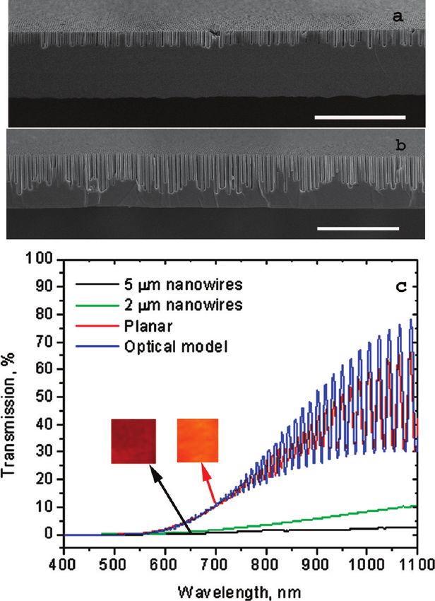
FIGURE 1. Ordered silicon nanowire array fabrication scheme. The fabrication consisted of three major steps depicted above: dip coating an
n-type silicon wafer in an aqueous suspension of silica beads to get a close-packed monolayer; deep reactive ion etching (DRIE) using the
beads as an etch mask to form nanowires; bead removal in HF and boron diffusion to form the radial p-n junction. Standard photolithography
and metal sputtering were used for the top finger grid while metal evaporation provided the back contact (not shown).

FIGURE 2. Solar cell fabrication and structure. (a) Scanning electron micrograph (SEM) of a close-packed monolayer of silica beads assembled
on a silicon wafer using dip coating. Scale bars are 10 and 1 µm for the main picture and inset, respectively. (b) Plan view SEM of a completed
ordered silicon nanowire radial p-n junction array solar cell made by bead assembly and deep reactive ion etching. The inset shows the edge
of a top contact finger, demonstrating that the metal completely fills in between the nanowires. Scale bars are 1 µm. (c) Tilted cross-sectional
SEM of the solar cell in panel b. Scale bar is 1 µm. (d) Tilted optical image of 36 silicon nanowire radial p-n junction solar cell arrays from
(a-c). The color dispersion demonstrates the excellent periodicity present over the entire substrate. Scale bar is 4 cm.

bead diameter, while the length is determined by the DRIE                   diffusion in silicon nanowires gives radial doping profiles that
time. Because of partial etching of the silica bead mask, the               match well with those calculated using standard diffusion
final nanowire diameter is always smaller than the starting                 equations.10 Photolithography and aluminum/palladium sput-
bead diameter and is coupled to the etch time; for our                      tering led to a top contact grid with metal filling completely
standard 8 min etch the diameter was 390 nm when using                      between the nanowires, which allowed for probing without
530 nm beads and the length was about 5 µm. After DRIE,                     breaking any nanowires (Figure 2b, inset).
the mask was removed with hydrofluoric acid and the radial                      Figure 2d shows an optical image of the completed
p-n junction was formed via boron diffusion into the                        devices on a 16 cm2 substrate; the iridescent color gradient
starting n-type silicon wafer. The junction depth was calcu-                is caused by white light interacting with the periodic nano-
lated to be about 160 nm. Our previous work has shown that                  wire array at different angles, demonstrating the excellent

     © 2010 American Chemical Society                                1083                      DOI: 10.1021/nl100161z | Nano Lett. 2010, 10, 1082-–1087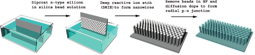
FIGURE 3. Solar cell output characteristics. (a) 5 µm nanowire and planar control solar cells fabricated from an 8 µm thin silicon absorber.
(b) The same structures as in panel a, but using a 20 µm thin silicon absorber.

uniformity over large areas that can be achieved with this                    The 4.83% average efficiency for the 8 µm absorber
technique. Each of the 36 solar cells located on the same                 silicon nanowire array solar cells is about 20% higher than
substrate is electrically isolated from the others by mechan-             results on 8 µm thick silicon ribbon solar cells, while the 20
ical sawing. As substrates for the dip coating and subsequent             µm absorber silicon nanowire cell average efficiency of
solar cell fabrication, we used very highly doped n-type                  5.30% is about 35% lower than equivalent ribbon cells,13
silicon wafers with two different doping levels, each with a              demonstrating that the nanowire geometry provides supe-
thin, lightly doped epitaxial layer on top. Since the minority            rior light trapping but also dramatically increases surface and
carrier diffusion length depends on the doping concentra-                 junction recombination. For very thin absorbing layers the
tion,11 these wafers allowed us to mimic the photovoltaic                 light-trapping effects dominate, while for thicker cells that
response of very thin silicon solar cellss8 and 20 µm in our              already absorb a large fraction of the incident light, the
caseswhile avoiding complications associated with handling                recombination effect is more important. Indeed, planar
such thin silicon wafers or depositing and contacting mul-                controls fabricated in parallel on the 8 µm silicon absorbing
ticrystalline silicon on a low-cost substrate. This simple                layer wafers showed a 4% lower Jsc versus the nanowire cells,
method for varying the silicon solar cell thickness also allows           but planar controls made using the 20 µm silicon absorbing
for quantitative measurements of the nanowire array’s light               layers had a 14% higher Jsc than nanowire cells. Previous
trapping efficiency, as will be discussed later. Even though              reports advocating silicon nanowire array solar cells have
low-cost substrates were not used in this proof-of-concept                shown they exhibit excellent antireflection properties but have
study, the fabrication procedure demonstrated here should                 not considered additional light-trapping effects.14-18 In order
be transferable to multicrystalline silicon (or even other                to explore the optical trapping advantages and recombina-
semiconductor) thin films deposited on low-cost substrates,               tion disadvantages of nanowire arrays, we have fabricated
such as glass, aluminum, or metallurgical grade silicon.12                arrays with the same periodicity but with different lengths
    Figure 3 shows the output characteristics of 5 µm nano-               on several different silicon absorbing layer thicknesses and
wire and planar control solar cells under AM1.5G illumina-                measured their optical transmission spectra and photovol-
tion for two different silicon absorber thicknesses. The                  taic characteristics.
average Voc and FF values of 0.519 ( 0.003 V and 0.607 (                      Figure 4 shows tilted cross-sectional SEM images and
0.005 for the 20 µm absorbing layer and 0.525 ( 0.002 V                   corresponding transmission measurements of thin silicon
and 0.559 ( 0.02 for the 8 µm absorbing layer are higher                  membranes patterned with nanowire arrays of two different
than previously reported values for silicon nanowire core-                lengths. The membranes were prepared by etching windows
shell p-n junction photovoltaics.6,7 The average Jsc values               in the handle of silicon on insulator (SOI) wafers through a
of 16.82 ( 0.50 and 16.45 ( 0.19 mA/cm2 give an overall                   silicon nitride mask using KOH. The buried oxide acts as an
efficiency of 5.30 ( 0.19% and 4.83 ( 0.19% for the 20                    etch stop, giving windows with only the thin silicon device
and 8 µm cells, respectively. The 2% increase in Jsc for the              layer remaining. The SOI device layer was chosen to have a
thicker nanowire cell is much smaller than the expected                   similar thickness to the 8 µm thin silicon absorber solar cells
20% increase calculated from the absorption for a single                  to allow for direct comparison. These wafers with thin silicon
pass through the different silicon layer thicknesses and the              windows were used for nanowire fabrication following the
22% increase shown in the planar control samples. This                    bead assembly and etching procedure discussed previously.
suggests the periodic vertical nanowire arrays provide a                  The standard 8 min etch yields nanowires that are about 5
strong light trapping effect, which will be discussed in detail           µm long so that most of the membrane has a nanowire
later.                                                                    structure, while the 4 min etch leads to about 2 µm short

     © 2010 American Chemical Society                              1084                     DOI: 10.1021/nl100161z | Nano Lett. 2010, 10, 1082-–1087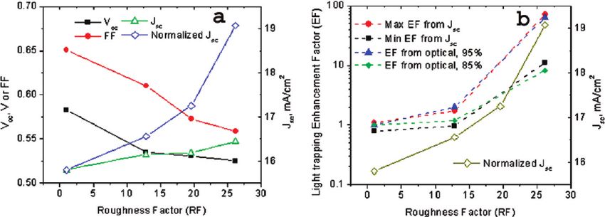
way to confirm that the periodic vertical nanowire array truly
                                                                             traps light and leads to increased absorption is to monitor
                                                                             the Jsc as a function of nanowire length for thin silicon solar
                                                                             cells that can benefit significantly from an increased effective
                                                                             path length.
                                                                                 Figure 5a shows the photovoltaic characteristics for 8 µm
                                                                             cells fabricated with various nanowire lengths, leading to
                                                                             different roughness factors. The roughness factor (RF) is
                                                                             defined as the actual surface area of the structure divided
                                                                             by the geometric area (e.g., RF of a planar cell is 1). The Voc,
                                                                             FF, and Jsc trends show that the increased surface and
                                                                             junction areas lead to both enhanced recombination (lower
                                                                             Voc, FF) and improved light trapping (higher Jsc). It also
                                                                             appears that the light-trapping effect dominates over the
                                                                             surface and junction recombination effect for this silicon
                                                                             absorber thickness, as the Jsc continues to increase with
                                                                             higher RF. The correlation between Jsc and RF is especially
                                                                             striking when considering that by increasing the nanowire
                                                                             length, the amount of silicon left to absorb light is decreasing
                                                                             significantly and a much higher fraction of the remaining
                                                                             silicon is in close proximity to the surface and p-n junction,
                                                                             increasing the probability of carrier recombination. In order
                                                                             to correct for the reduced volume, the Jsc was normalized
                                                                             by the fraction of light that should be absorbed as compared
                                                                             to the planar control (Figure 5a, normalized Jsc).
                                                                                 The RF-dependent recombination effect was removed by
                                                                             comparing the Jsc of silicon nanowire array solar cells with
                                                                             the same RF, and thus the same surface and junction
FIGURE 4. Optical transmission measurements on thin silicon                  recombination characteristics, but with different absorbing
windows with and without nanowires. Tilted cross-sectional SEM
images of (a) 2 µm nanowire arrays and (b) 5 µm nanowire arrays
                                                                             layer thicknesses. In this way, we can quantitatively extract
on 7.5 µm thick silicon windows. Both scale bars are 10 µm. (c)              light-trapping path length enhancement factors (EF) for
Transmission spectra of thin silicon window structures before (red)          different nanowire geometries (full derivation in Supporting
and after etching to form 2 µm (green) and 5 µm (black) nanowires.
The spectra from an optical model for a 7.5 µm thin silicon window
                                                                             Information). Figure 5b shows the minimum and maximum
is in blue and matches very well with the planar control measure-            EF as a function of RF plotted on a semilog scale compared
ment. The insets are backlit color images of the membranes before            to the normalized Jsc from Figure 5a on a linear scale. The
and after etching. Clearly there is a large intensity reduction and
red shift in the transmitted light after the nanowires are formed,
                                                                             strong correlation further supports the light-trapping effect,
suggesting strong light trapping.                                            as the absorption (and thus Jsc) should increase logarithmi-
                                                                             cally with the path length. The transmission measurements
nanowires that penetrate into only the top 25% of the                        in Figure 4c can also be used to calculate an EF as a function
membrane (Figure 4). Optical measurements performed on                       of RF. In this case, there is uncertainty as to how much of
these membranes before and after nanowire fabrication                        the reduced transmission comes from absorption versus
show that the transmission over the entire spectral range                    how much is from scattered light that does not couple into
from 600 to 1100 nm is reduced by factors of 2.9-7.8 and                     the cell and is ultimately lost. From the photocurrent data,
12-29 for the 2 and 5 µm nanowires, respectively (Figure                     the light-trapping efficiency clearly increases with RF, so we
4c). The planar control shows strong interference patterns                   would expect that the fraction of scattered light that leads
and is in excellent agreement with an optical model for a                    to absorption would also increase with RF. If we assume this
7.5 µm thin silicon membrane (details in Supporting Infor-                   coupling efficiency is proportional to the logarithm of RF and
mation). The insets in Figure 4c show backlit color images                   set a coupling efficiency of 95% (after reflection losses) for
of the windows with and without nanowires; clearly the                       the longest nanowires, then we get EF of 2.0 and 62 for the
nanowire arrays reduce the intensity and red shift the                       shortest and longest nanowires, respectively, in excellent
frequency of the transmitted light, as expected for a strong                 agreement with the maximum EF from the Jsc data that
light-trapping effect. It is possible that the nanowires simply              varied between 1.7 and 73 (Figure 5). If instead we assume
act as very effective scattering centers and that some (or                   an 85% coupling efficiency, we get EF of 1.2 and 8.3 for the
even a majority) of the light is coupled out of the membrane                 shortest and longest nanowires, respectively, close to the
at some angle so that it does not strike the detector. One                   minimum EF from the Jsc data of 0.96 and 11. This demon-

     © 2010 American Chemical Society                                 1085                     DOI: 10.1021/nl100161z | Nano Lett. 2010, 10, 1082-–1087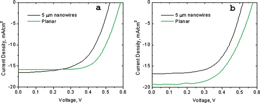
FIGURE 5. Photovoltaic response and light-trapping effect as a function of roughness factor. (a) The Voc, FF, and Jsc of periodic silicon nanowire
array solar cells fabricated from an 8 µm thick silicon absorber with three different roughness factors (RF) compared to a planar control (RF
) 1). The normalized Jsc is determined by dividing the nanowire Jsc by the fraction of light that should be absorbed compared to the planar
control, considering the loss in volume for the nanowire cells. The increasing Jsc with higher RF suggests that the light trapping effect induced
by ordered nanowire arrays is sufficient to overcome the increased surface and junction recombination that comes with longer nanowires.
(b) Light-trapping path length enhancement factor (EF) vs RF on a semilog scale derived by comparing the Jsc from ordered silicon nanowire
arrays with the same RF but different absorber thicknesses (red and black) and from the optical transmission measurements in Figure 3c,
assuming 95% (blue) or 85% (green) of the reduced transmission ultimately leads to absorption. The normalized Jsc (brown) is also shown on
a linear scale for comparison. The strong correlation further supports the light-trapping effect since absorption (and ultimately photocurrent)
scales with the logarithm of the path length.

strates that there is very good coupling and an extraordinary                    In conclusion, we have demonstrated a simple and scal-
light-trapping effect, exceeding the theoretical maximum of                  able method to fabricate large-area silicon nanowire radial
2n2 (∼25 for Si), where n is the refractive index, for ideal                 p-n junction photovoltaics. It requires dip coating a silicon
randomizing (Lambertian) schemes without a back reflec-                      substrate to self-assemble silica spheres, DRIE to form
tor.19-21 It is important to recognize that these extraordinary              nanowires and diffusion to form the p-n junction. We
EF results include the entire AM1.5G spectrum (above the                     achieved efficiencies of between 5 and 6% for these ordered
silicon band gap), suggesting that the EF at wavelengths near                vertical silicon nanowire array solar cells on 20 and 8 µm
the band gap must be much higher. Indeed, using the                          silicon absorber layers with different roughness factors. By
transmission measurements as described above gives EF of                     comparing the photovoltaic output characteristics of these
156-210 at 1050 nm for 85-95% coupling efficiency.                           different cells, we show that longer nanowires lead to both
    Calculations have shown that certain periodic structures                 increased recombination and higher absorption, with the
are capable of exceeding the Lambertian EF limit,20,22-24                    light-trapping effect dominating for 8 µm thin silicon absorb-
including orthogonal grooves on opposite sides of a silicon                  ing layers. We quantitatively measure a maximum light
slab (EF 50-70)20 and photonic crystals coupled to a planar                  trapping path length enhancement factor over the entire
absorber (EF >100 for certain wavelength ranges).22 One                      AM1.5G spectrum between 1.7 and 73, depending on the
study predicted a maximum EF for solar cells coupled to                      nanowire geometry, which agrees well with enhancement
photonic crystals consisting of silicon pillars with a period                factors between 2 and 62 extracted from optical transmis-
of approximately 500 nm and a diameter of 390 nm, nearly                     sion measurements. This light-trapping ability is above the
identical to what we have produced here (though they                         theoretical limit for a randomizing scheme, indicating that
examined a square lattice and our structures have a hex-                     there may be photonic crystal enhancement effects present
agonal lattice).22 However, without comparing arrays of                      in our devices. This ordered vertical nanowire array geom-
different periods and even random spacing, we cannot                         etry represents a viable path toward high-efficiency, low-cost
conclusively say that our cells show a photonic crystal                      thin-film solar cells by providing a way to reduce both the
enhancement effect. Despite the incredible light trapping,                   quantity and quality of the required semiconductor.
these nanowire structures still do not exceed the overall
efficiency of planar cells, at least for silicon layers above 8
                                                                               Acknowledgment. We thank Akram Boukai and Sarah
µm in thickness, due to enhanced surface and junction
                                                                             Brittman for reviewing the manuscript. NSF-COINS provided
recombination. We did not perform any surface passivation,                   funding for this project. P.Y. would like to thank NSF for the
which is known to be important in high-performance planar                    Waterman Award.
solar cells and should be even more critical for these devices.
Proper surface treatments and improved nanowire array                          Supporting Information Available. Methods, enhance-
geometries that allow for lower roughness factors without                    ment factor, and planar transmission model calculation
sacrificing light trapping will be critical to achieve high                  details. This material is available free of charge via the
efficiency ultrathin silicon solar cells.                                    Internet at http://pubs.acs.org.

     © 2010 American Chemical Society                                 1086                      DOI: 10.1021/nl100161z | Nano Lett. 2010, 10, 1082-–1087
REFERENCES AND NOTES (12) Green, M. A.; et al. Sol. Energy 2004, 77, 857–863.
(1) Lewis, N. S.; Nocera, D. G. Proc. Natl. Acad. Sci. U.S.A. 2007, 104, (13) Yoon, J.; et al. Nat. Mater. 2008, 7, 907–915.
20142–20152. (14) Peng, K. Q.; et al. Small 2005, 1, 1062–1067.
(2) Fawer-Wasswer, M. Solar energyssunny days ahead? Current (15) Fang, H.; Li, X. D.; Song, S.; Xu, Y.; Zhu, J. Nanotechnology 2008,
status and outlook for photovoltaics and solar thermal power. 19, 255703.
Sarasin Sustainable Investment Report, 2004. (16) Zhu, J.; et al. Nano Lett. 2009, 9, 279–282.
(3) Green, M. A. Sol. Energy 2004, 76, 3–8. (17) Hu, L.; Chen, G. Nano Lett. 2007, 7, 3249–3252.
(4) Alsema, E. A. Prog. Photovoltaics 2000, 8, 17–25. (18) Muskens, O. L.; Rivas, J. G.; Algra, R. E.; Bakkers, E. P. A. M.;
(5) Kayes, B. M.; Atwater, H. A.; Lewis, N. S. J. Appl. Phys. 2005, 97, Lagendijk, A. Nano Lett. 2008, 8, 2638–2642.
114302. (19) Yablonovitch, E.; Cody, G. D. IEEE Trans. Electron Devices 1982,
(6) Tian, B. Z.; et al. Nature 2007, 449, 885–888. 29, 300–305.
(7) Garnett, E. C.; Yang, P. J. Am. Chem. Soc. 2008, 130, 9224–9225. (20) Campbell, P.; Green, M. A. J. Appl. Phys. 1987, 62, 243–249.
(8) Bogush, G. H.; Tracy, M. A.; Zukoski, C. F. J. Non-Cryst. Solids (21) Green, M. A. Silicon Solar Cells: Advanced Principles & Practice;
1988, 104, 95–106. University of New South Wales, 1995.
(9) Hsu, C.; Connor, S. T.; Tang, M. X.; Cui, Y. Appl. Phys. Lett. 2008, (22) Zhou, D. Y.; Biswas, R. J. Appl. Phys. 2008, 103, No. 093102.
93, 133109. (23) Chutinan, A.; Kherani, N. P.; Zukotynski, S. Opt. Express 2009,
(10) Garnett, E. C.; et al. Nat. Nanotechnol. 2009, 4, 311–314. 17, 8871–8878.
(11) Delalamo, J. A.; Swanson, R. M. Solid-State Electron. 1987, 30, (24) Bermel, P.; Luo, C.; Zeng, L.; Kimerling, L. C.; Joannopoulos, J. D.
1127–1136. Opt. Express 2007, 15, 16986–17000.
© 2010 American Chemical Society 1087 DOI: 10.1021/nl100161z | Nano Lett. 2010, 10, 1082-–1087You can also read