Holey Silicon as an Efficient Thermoelectric Material
←
→
Page content transcription
If your browser does not render page correctly, please read the page content below
pubs.acs.org/NanoLett

Holey Silicon as an Efficient Thermoelectric
Material
Jinyao Tang,†,§,⊥ Hung-Ta Wang,†,⊥ Dong Hyun Lee,| Melissa Fardy,† Ziyang Huo,†
Thomas P. Russell,| and Peidong Yang*,†,‡,§
†
 Department of Chemistry and ‡ Department of Materials Science and Engineering, University of California,
Berkeley, California 94720, § Materials Sciences Division, Lawrence Berkeley National Laboratory,
Berkeley, California 94720, and | Department of Polymer Science and Engineering, University of Massachusetts,
Amherst, Massachusetts 01003

    ABSTRACT This work investigated the thermoelectric properties of thin silicon membranes that have been decorated with high density
    of nanoscopic holes. These “holey silicon” (HS) structures were fabricated by either nanosphere or block-copolymer lithography,
    both of which are scalable for practical device application. By reducing the pitch of the hexagonal holey pattern down to 55 nm with
    35% porosity, the thermal conductivity of HS is consistently reduced by 2 orders of magnitude and approaches the amorphous limit.
    With a ZT value of ∼0.4 at room temperature, the thermoelectric performance of HS is comparable with the best value recorded in
    silicon nanowire system.

    KEYWORDS Silicon, thermoelectric, thermal conductivity, necking, nanostructure

S      olid state thermoelectric (TE) modules convert heat                          for large scale implementation. The thermal transport prop-
       to electricity and are commonly used for cooling and                         erties of silicon nanowires not only highly depend on its
       refrigeration purposes.1-4 Current research has been                         diameter/size,12,14,15 but also on their nanoscopic surface
directed toward nanoscale materials due to the potential of                         morphology.12 Thus, the synthesis of high density and highly
enhancing the Seebeck coefficient and suppressing the                               uniform nanostructures is a key challenge for realizing high
thermal conductivity.5-8 The most widely used thermoelec-                           performance silicon nanowire-based TE modules.
tric material, Bi2Te3, has the figure of merit ZT () S2σT/κ) ∼                         To overcome these problems inherent to the nanowire
1 at room temperature, where S is Seebeck coefficient, σ is                         system, we report here the enhanced thermoelectric per-
electrical conductivity, T is the absolute temperature, and κ                       formance of a new type of nanostructure, holey silicon (HS),
is thermal conductivity. Its application in energy generation                       where high density nanoscopic holes are created in thin,
is limited, however, mainly due to the materials limited                            single-crystalline silicon membranes. These HS nanostruc-
availability, low stability, and high manufacturing cost. Bulk                      tures exhibit good mechanical strength and reproducibly low
silicon, which is abundant and well-engineered, has never                           thermal conductivity while maintaining sufficient electrical
been considered for TE applications due to its high lattice                         quality. These characteristics make them viable candidates
thermal conductivity (150 W/m·K).9 On the other hand,                               for TE applications. HS was prepared using either nano-
porous silicon with randomly distributed and intertwined                            sphere lithography (NSL) or block copolymer (BCP) lithog-
pores could achieve extremely low thermal conductivity                              raphy, yielding holes with pitches of 350, 140, and 55 nm.
down to 0.1 W/m·K.10 However, the electronic structure of                           Our results show that the thermal conductivity of 55 nm
this disordered porous silicon is severely deteriorated, which                      pitch HS can be as low as 1.14-2.03 W/m·K. In the HS
yields very poor electrical conductivity and thus a low ZT.11                       system reported here, we propose that a “necking effect” is
Recent work has shown that by either using nanowires with                           the main mechanism of reducing thermal conductivity based
diameters much smaller than the bulk phonon mean free                               on our experiments and previously reported simulation.16
path (MFP) or roughening the nanowire surface, a near 100-                          Without significantly sacrificing the thermoelectric power
fold suppression in lattice thermal conductivity is observed,                       factor, S2σ, we demonstrate that HS behaves like a phonon
resulting in a ZT that is dramatically enhanced from 0.01                           glass and electron crystal17 with ZT ∼ 0.4 at room temper-
for the bulk to 0.4-0.6.12,13 However, Si nanowires’ weak                           ature. Additional improvement could be achieved by further
mechanical strength and strong dependence on both diam-                             optimization of the electrical doping, as well as the pitch and
eter and detailed surface morphology remain as challenges                           porosity of the holes. The scalability of the BCP lithography
                                                                                    process and the promising thermoelectric properties make
                                                                                    HS superior for practical thermoelectric power generation.
* To whom correspondence should be addressed. E-mail: p_yang@berkeley.edu.
⊥
                                                                                       The preparation of large scale HS films is based on deep
  These authors contributed equally to this work.
Received for review: 08/18/2010                                                     reactive ion etching (DRIE) of silicon-on-insulator (SOI)
Published on Web: 09/14/2010                                                        substrates (100 nm device layer, confirmed by scanning

      © 2010 American Chemical Society                                       4279                      DOI: 10.1021/nl102931z | Nano Lett. 2010, 10, 4279–4283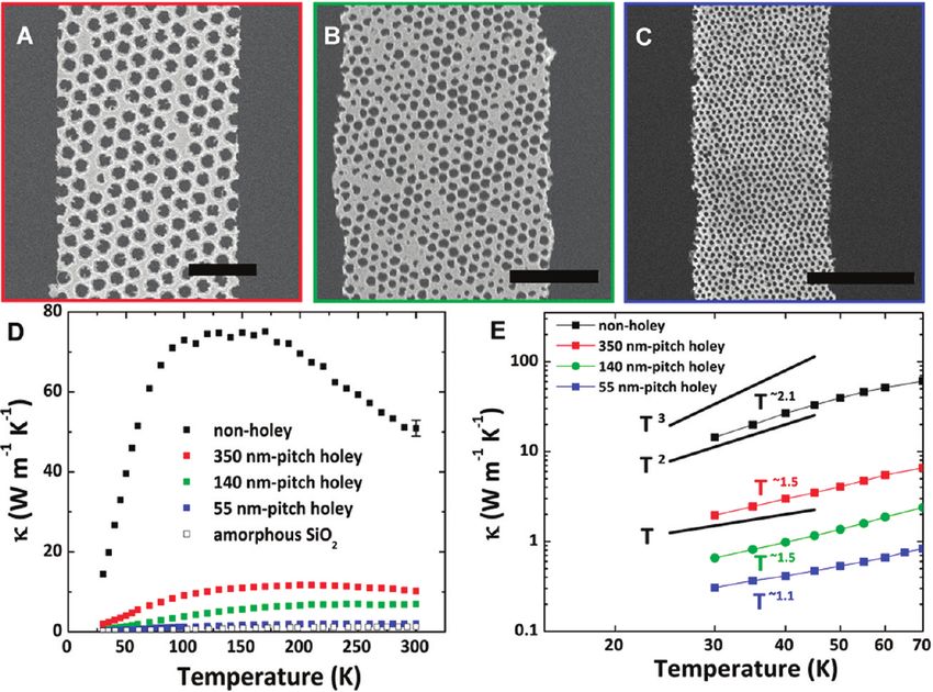
FIGURE 1. Structural characterization of 55 nm pitch HS ribbon. (A) AFM topography image of BCP holey pattern with Fourier-transform
pattern (inset) indicating the long-range order. (B) Bright-field TEM image of a section of HS ribbon. The porosity is estimated as ∼35% through
the entire ribbon. SAED pattern (inset) indicates its single crystalline nature. (C) High-resolution TEM of the edge of a hole showing ∼2 nm
thick surface native oxide. (D) SEM image of the thermal measurement device. Between two suspended SiNx membranes, a 55 nm pitch HS
ribbon is bonded by 300 nm Ni. Scale bars for panels A and B are 1 µm, panel C is 5 nm, and panel D is 10 µm.

electron microscopy (SEM) cross section) masked by thin                     SOI device layer. The sidewalls of the holes have a layer of
chromium masks templated by either NSL or self-assembled                    1-2 nm native oxide, as shown in Figure 1C.
BCP film (details in Supporting Information). This method                      The thermal transport properties of the HS ribbon were
yields uniform 55, 140, or 350 nm pitch HS with porosity                    characterized by microelectromechanical systems (MEMS)
of ∼35%. Specifically for 55 nm pitch HS, the self-assembled                devices,18 which consist of two suspended silicon nitride
BCP holey pattern (Figure 1A) is transferred to the HS film
                                                                            (SiNx) membranes patterned with platinum heating/sensing
through DRIE. For transport measurements and SEM/
                                                                            coils and separated by 10-30 µm. The HS ribbons were
transmission electron microscopy (TEM) characterization, all
                                                                            placed between the two membranes using a micromanipu-
HS films were tailored into individual ribbons (1-3 µm ×
                                                                            lator, then anchored to the membrane by a ∼300 nm thick
20-50 µm) by standard photolithography, then released
from the SOI substrate by etching the buried oxide layer in                 Ni bonding patch that was evaporated through a SiNx stencil
hydrofluoric acid vapor. The TEM image (Figure 1B) shows                    mask (Figure 1D). The thermal contact resistance was
that the HS ribbon has uniform hole size and separation with                estimated by comparing the thermal conductance of Ni
ordered hexagonal packing. As shown in Figure 1B inset, the                 bonded silicon ribbon to monolithically integrated silicon
selected area electron diffraction (SAED) pattern recorded                  ribbon (Figure S4, Supporting Information) and was con-
along the [100] zone axis confirms the single-crystallinity of              firmed to be less than 10% of total resistance for all the HS
the entire HS ribbon, which is consistent with the starting                 ribbons measured (Figure 2A-C).

     © 2010 American Chemical Society                                4280                      DOI: 10.1021/nl102931z | Nano Lett. 2010, 10, 4279-–4283
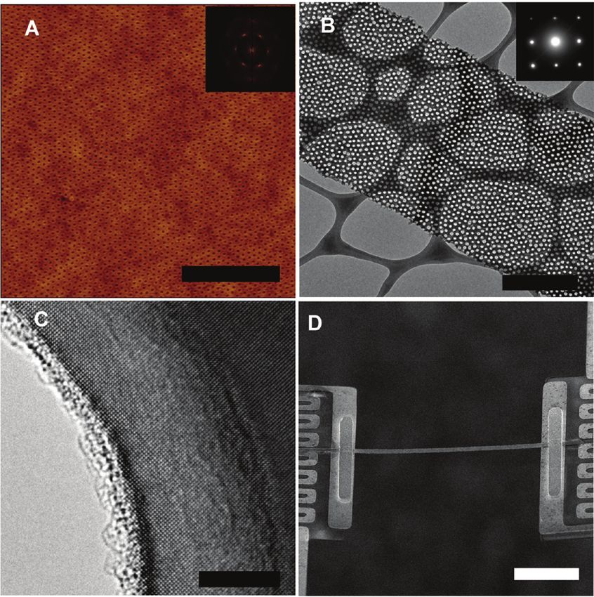
FIGURE 2. Thermal conductivity of HS ribbons with different pitch. SEM images of (A) 350 nm pitch, (B) 140 nm pitch, and (C) 55 nm pitch
HS ribbon for thermal measurement. All scale bars are 1 µm. (D) Temperature dependent K of nonholey (black squares), 350 nm (red squares),
140 nm (green squares), 55 nm pitch (blue squares) HS ribbon, and amorphous silica (empty squares from ref 19). Error bars for all three
holey ribbons are smaller than the data points. (E) Low-temperature data on a logarithmic scale with T3, T2, and T1 curves for comparison
guidelines.

   Figure 2D shows the temperature dependent thermal
                                                                         TABLE 1. Summary of the HS Geometry and the Thermal
conductivity of HS with different pitches in comparison to a
                                                                         Conductivity at 300 Ka
nonholey ribbon and amorphous silica.19 The room tem-
perature thermal conductivities of all silicon ribbons are also
summarized in Table 1 for comparison. With similar porosity
( ∼ 35%), the HS ribbons show a clear trend of thermal
conductivity reduction as a function of pitch size. This
dependency deviates from the classic Eucken model,20
κporous/κsolid ) (1 - )/(1 + /2), indicating κ should be 42W/
m·K for all 35% HS, which is only valid when the material
                                                                                      avg. pitch,   avg. neck,    avg. porosity,
dimensions are much larger than the phonon MFP. The
                                                                                        p (nm)        n (nm)           (%)          κ (Wm-1 K-1)
dramatic discrepancy to the Eucken model across the entire
                                                                         nonholey                                        0            50.9 ( 2.0
temperature range demonstrates that phonon size effect is                nonholey*                                       0            47.6 ( 1.7
very important among these HS dimensions and will be                     350-pitch       350           152             ∼35           10.23 ( 0.44
discussed latter. In addition, the peak of the thermal con-              140-pitch       140            59             ∼35            6.96 ( 0.34
                                                                         55-pitch         55            23             ∼35            2.03 ( 0.07
ductivity versus temperature curve (Umklapp peak) is shifted
                                                                         55-pitch*        55            23             ∼35            1.73 ( 0.06
to higher temperature as the pitch size decreases, suggesting
                                                                           a
phonon-phonon scattering contributes minimally in limit-                     Note: All ribbons are 100 nm in thickness. All κ are normalized
                                                                         by . Samples are all intrinsic (phosphorus doped, ∼3 × 1014 cm-3),
ing the thermal transport in these structure (TU-peak ∼ 130 K            except * (boron doped, ∼5 × 1019 cm-3) used for ZT.
for nonholey ribbon, TU-peak ∼ 200 K for 350 nm pitch HS,
and TU-peak > 300 K for both 140 nm and 55 nm pitch HS.).                size effect in the holey structure presented here is quite
In Figure 2E, we further compare the temperature depend-                 important and can effectively suppress thermal conductivity
ent thermal conductivity at low-temperature region (30-60                beneficial for TE application.
K), and a clear trend on temperature power rule (T3 for bulk)               It can be seen that the thermal conductivity of the 55 nm
is also observed indicating specific scattering effect is de-            pitch HS is comparable to that of amorphous silica.19 To
creasing the temperature power to ∼1.1 for 55 nm HS.15                   verify the reproducibility of the low thermal conductivity in
These intriguing thermal properties imply that the phonon                HS, multiple samples are prepared in different batches, and

     © 2010 American Chemical Society                             4281                       DOI: 10.1021/nl102931z | Nano Lett. 2010, 10, 4279-–4283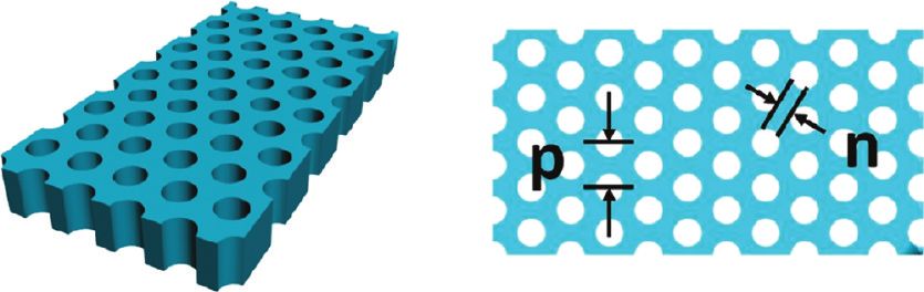
consistently low values, ranging from 1.14 to 2.03 W/m·K                  with differing neck widths, ranging from 160 to 40 nm, by
at room temperature, are routinely recorded (see Figure S5,               changing porosity from 13 to 40%. After normalizing the
Table S1 in Supporting Information for detail). The cause of              porosity, the results clearly show that the thermal conductiv-
variation is mainly due to the slight difference in porosity              ity decreases with neck width. (see also Supporting Informa-
among samples, resulting from the block copolymer quality                 tion Figure S6, compared in parallel with theoretical predic-
and etching conditions. Also, no dependence of the thermal                tion). It is also worth mentioning that the imperfection of
conductivity on ribbon width, ranging from 0.79 to 2.35 µm,               holes packing in our HS could potentially introduce ad-
is observed, suggesting that the phonon transport is domi-                ditional scattering on broader range of phonon spectra,
nated by the HS morphology. This represents a distinct                    which is beneficial for κ reduction.
advantage of HS over nanowire systems, in which the                           Since the electron MFP in highly doped silicon (∼1 × 10¹⁹
performance varies significantly with diameter and detailed               cm-3, optimal for thermoelectric application) is ∼1-10 nm,
surface morphology.12,13                                                  which is smaller than the 55 nm pitch, there should be no
    Compared with silicon nanowires, one key feature of the               analogous necking effect on the electrical properties. There-
HS structure is that the width of thinnest part, or neck (n), is          fore, the power factor (S2/F) of HS should not be degraded,
considerably less than the pitch size (p), such that n/p ∼ 0.42           resulting in a net increase in ZT. To this end, we measured
for samples with 35% porosity. This geometry is very                      all the thermoelectric properties (S, F, and κ) of the 55 nm
different to nanowires, wherein the surface roughness (h) is              pitch HS to evaluate its ZT. The SOI were doped with boron
much less than its diameter (d), making h/d < 0.1.12 For 55               at 830 °C for 1 h in a customized BCl3 doping furnace to
nm pitch HS with 35% porosity, the neck is approximately                  achieve a doping level ∼5 × 1019 cm-3 (confirmed by hall
20 nm in width. However, this 55 nm pitch HS gives                        measurement), then 55 nm pitch HS ribbon was prepared
significantly lower thermal conductivity than that of 22 nm               as described previously. Four probe electrical contacts paral-
silicon nanowire, reported previously as ∼7 W/m·K.14,15 In                lel to a platinum heating coil were patterned using photoli-
our HS system where n/p is much larger, phonons could                     thography for both F and S measurements (device details
experience more backscattering by reflecting from the                     are shown in Figure S7 and Supporting Information; the
nanohole sidewalls. We propose that this feature plays an                 result is shown in Figure S4A). The postdoped HS showed a
important role in dramatically decreasing the thermal                     thermal conductivity of ∼1.73 W/m·K at room temperature,
conductivity.                                                             not significantly different from the undoped holey ribbons
    Several theoretical studies have been reported on similar             (Table 1). With this doping concentration, the electronic
porous structure.8,16,21 In particular, Hao et al. reported a             contribution of thermal conductivity, κe ) LTσ is about 0.21
Monte Carlo simulation of phonon transport in silicon with                W/m·K (Lorenz number, L ) 2.2 × 10⁻⁸ J2K-2C-2, is defined
square arrays of holes considering frequency dependent                    by Wiedemann-Franz law for degenerate doping), leading
phonon MFP, which increased the accuracy of their model.16                to a lattice thermal conductivity, κph of 1.52 W/m·K.
The trend of pitch dependent thermal conductivity reduction                   For comparison, Figure 3B shows the ratios of the thermal
experimentally shown in the HS system is similar to the                   conductivity κ and thermoelectric power factor S2/F for holey
model result, yet the experimental value is smaller than the              and nonholey controls as a function of temperature. The HS
prediction. We attribute the difference to the surface scat-              shows 34 times suppression of thermal conductivity com-
tering in 100 nm thick film, porosity difference, small surface           pared with the nonholey silicon ribbons and 85 times
roughness created by the DRIE, and the difference between                 suppression compared with bulk silicon at room tempera-
square array and hexagonal array (see details in Figure S6                ture with greater decreases observed at lower temperature
and Supporting Information). Their simulation suggested                   in both cases. A moderate deterioration of the thermoelectric
that when the distance of adjacent holes is smaller than                  power factor is also observed as compared with optimally
phonon MFP, a phonon can be “trapped” behind the hole,                    doped nonholey Si ribbons (Note both κ and F of HS are
which creates a local negative temperature gradient oppos-                normalized by porosity). The lower thermoelectric power
ing the linear temperature gradient along a free channel. We              factor is mainly due to the decreased electrical conductivity
address this phenomenon as a “necking effect”, which                      from carrier depletion by surface states. This is confirmed
requires necking morphology with pitch size being smaller                 experimentally as the electrical conductivity enhancement
than the phonon MFP. Additionally, it induces two distin-                 is observed by surface passivation with atomic layer deposi-
guishing thermal behaviors observed in our experiment.                    tion of Al2O3, and is currently under investigation for ad-
First, as the HS pitch size gets smaller, the percentage of               ditional ZT enhancement.
phonons with MFP (frequency dependent) greater than the                       Over the entire temperature range of our measurements,
pitch will increase, which should result in a stronger necking            the ZT enhancement factor remains ∼50 times in compari-
effect and lower overall κ, as is the trend observed in Figure            son to nonholey silicon of the same thickness (Figure 3C).
2. Second, the necking effect should become more signifi-                 From 150 to 300 K, the ZT of HS increases with temperature
cant as the “neck” become thinner while maintaining a fixed               and is 0.4 at 300 K. Comparing with thin and rough silicon
pitch. To verify this effect, 350 nm pitched HS was prepared              nanowire systems, these HS nanostructures exhibit reliable

     © 2010 American Chemical Society                              4282                     DOI: 10.1021/nl102931z | Nano Lett. 2010, 10, 4279-–4283
pitch/neck ratio, and effective surface passivation. Because
of the scalability of this process, an immediate application
for these holey silicon nanostructures could be on-chip
thermal management for solid state devices, while large
scale waste heat recovery is also conceivable by extension
to bulk materials system.
Acknowledgment. We thank R. Chen, S. Andrews, K.
Hippalgaonkar, J. Moore, and A. Majumdar for the discus-
sions and E. Garnett for the fabrication assistance. This work
was supported by the Director, Office of Basic Energy
Sciences, Materials Sciences and Engineering Division, of the
U.S. Department of Energy under Contract No. DE-AC02-
05CH11231 and under contract No. DE-FG02-96ER45612.
Supporting Information Available. Holey silicon fabrica-
tion, block copolymer (BCP) assembly and characterization,
thermal conductivity measurement and thermal contact
resistance calibration, thermal conductivity of HS and com-
parison with theory, electrical measurement, and additional
references. This material is available free of charge via the
Internet at http://pubs.acs.org.
REFERENCES AND NOTES
(1) DiSalvo, F. J. Science 1999, 285 (5428), 703–706.
(2) Tritt, T. M.; Zhang, B.; Gothard, N.; He, J.; Ji, X.; Thompson, D.;
Kolis, J. W. Mater. Res. Soc. Symp. Proc. 2006, 886, 53–63.
(3) Bell, L. E. Science (Washington, D.C.) 2008, 321 (5895), 1457–
1461.
(4) Snyder, G. J.; Toberer, E. S. Nat. Mater. 2008, 7 (2), 105–114.
(5) Hicks, L. D.; Dresselhaus, M. S. Phys. Rev. B 1993, 47 (24), 16631.
(6) Hicks, L. D.; Dresselhaus, M. S. Phys. Rev. B 1993, 47 (19), 12727–
12731.
(7) Cahill, D. G.; Ford, W. K.; Goodson, K. E.; Mahan, G. D.;
Majumdar, A.; Maris, H. J.; Merlin, R.; Phillpot, S. R. J. Appl.
Phys. 2003, 93 (2), 793–818.
(8) Yang, R.; Chen, G.; Dresselhaus, M. S. Phys. Rev. B: Condens.
Matter 2005, 72 (12), 125418/1–125418/7.
(9) Weber, L.; Gmelin, E. Appl. Phys. A 1991, A53 (2), 136–40.
(10) Gesele, G.; Linsmeier, J.; Drach, V.; Fricke, J.; Arens-Fischer, R. J.
Phys. D: Appl. Phys. 1997, 30 (21), 2911–2916.
(11) Yamamoto, A.; Takazawa, H.; Ohta, T. Int. Conf. Thermoelectr.
1999, 18th, 428–431.
FIGURE 3. Thermoelectric properties and ZT calculation for 55 nm (12) Hochbaum, A. I.; Chen, R.; Delgado, R. D.; Liang, W.; Garnett,
pitch HS ribbon. (A) Temperature-dependent G (black squares) and E. C.; Najarian, M.; Majumdar, A.; Yang, P. Nature (London) 2008,
S (red squares) of a boron doped 55 nm pitch HS ribbon. (hole 451 (7175), 163–167.
concentration ∼5 × 1019 cm-3 from hall measurement). The room (13) Boukai, A. I.; Bunimovich, Y.; Tahir-Kheli, J.; Yu, J.-K.; Goddard,
temperature S2/G ) 2.28 ( 0.59 mW/m·K. (B) K comparison of doped W. A., III; Heath, J. R. Nature (London) 2008, 451 (7175), 168–
55 nm pitch HS ribbon with doped nonholey silicon ribbon (black 171.
squares), or bulk silicon (open squares, 1.7× 1019 cm-3, As-doped, (14) Li, D.; Wu, Y.; Kim, P.; Shi, L.; Yang, P.; Majumdar, A. Appl. Phys.
from ref 9); S2/G comparison (red squares) of doped 55 nm pitch HS Lett. 2003, 83 (14), 2934–2936.
ribbon with nonholey silicon ribbon. (C) ZT of 55 nm pitch HS ribbon (15) Chen, R.; Hochbaum, A. I.; Murphy, P.; Moore, J.; Yang, P.;
(red squares) compared with nonholey ribbon (blue squares) shows Majumdar, A. Phys. Rev. Lett. 2008, 101 (10), 105501/1–105501/
∼50 times enhancement. With consideration of measurement error 4.
from both G (4.7%), S (3%), and K (6%), the ZT shows 16.7% (16) Hao, Q.; Chen, G.; Jeng, M.-S. J. Appl. Phys. 2009, 106 (11),
uncertainty at 95% confidence. 114321/1–114321/10.
(17) Slack, G. A. CRC Handbook of Thermoelectrics; Rowe, D. M., Ed.;
thermoelectric performance due to the necking effect while CRC Press: Boca Raton, FL, 1995; pp 407-40.
having much better mechanical strength. As mentioned (18) Shi, L.; Li, D.; Yu, C.; Jang, W.; Kim, D.; Yao, Z.; Kim, P.;
Majumdar, A. J. Heat Transfer 2003, 125 (5), 881–888.
above, the thermoelectric properties of these holey silicon (19) Cahill, D. G.; Pohl, R. O. Phys. Rev. B: Condens. Matter 1987, 35
nanostructures have no dependence on ribbons width, (8, Pt. 1), 4067–73.
making them even more amenable for TE module integra- (20) (a) Eucken, A. Ceram. Abstr. 1932, 11, 576. (b) Eucken, A. Ceram.
Abstr. 1933, 12, 231.
tion. Higher ZT values than the one reported here can be (21) Lee, J.-H.; Galli, G. A.; Grossman, J. C. Nano Lett. 2008, 8 (11),
obtained by further optimization of the doping level, the 3750–3754.
© 2010 American Chemical Society 4283 DOI: 10.1021/nl102931z | Nano Lett. 2010, 10, 4279-–4283You can also read