THEORETICAL ANALYSIS OF THE EFFECT OF THE INTERFACIAL MOSE2 LAYER IN CIGS-BASED SOLAR CELLS - SCIENTIFIC RESEARCH PUBLISHING
←
→
Page content transcription
If your browser does not render page correctly, please read the page content below
Open Journal of Modelling and Simulation, 2021, 9, 339-350
                                                                                              https://www.scirp.org/journal/ojmsi
                                                                                                          ISSN Online: 2327-4026
                                                                                                            ISSN Print: 2327-4018

Theoretical Analysis of the Effect of the
Interfacial MoSe2 Layer in CIGS-Based Solar
Cells

Adama Sylla1, N’Guessan Armel Ignace1, Touré Siaka1, Jean-Pierre Vilcot2
1
 Laboratoitre d’Energie Solaire, Université Félix Houphouët Boigny, Abidjan, Côte d’Ivoire.
2
 Institut d’Electronique, de Microélectronique et de Nanotechnologie (IEMN), UMR, CNRS, 8520. Laboratoire Central, Villeneuve
d’Ascq Cedex, Lille, France

How to cite this paper: Sylla, A., Ignace,    Abstract
N.A., Siaka, T. and Vilcot, J.-P. (2021)
Theoretical Analysis of the Effect of the     The aim of this work is to analyze the influence of the interfacial MoSe2 layer
Interfacial MoSe2 Layer in CIGS-Based         on the performance of a /n-ZnO/i-ZnO/n-Zn(O,S)/p-CIGS/p+-MoSe2/Mo/SLG
Solar Cells. Open Journal of Modelling and
Simulation, 9, 339-350.
                                              solar cell. In this investigation, the numerical simulation software AFORS-
https://doi.org/10.4236/ojmsi.2021.94022      HET is used to calculate the electrical characteristics of the cell with and with-
                                              out this MoSe2 layer. Different reported experimental works have highlighted
Received: July 20, 2021
                                              the presence of a thin-film MoSe2 layer at the CIGS/Mo contact interface.
Accepted: August 27, 2021
Published: August 30, 2021                    Under a tunneling effect, this MoSe2 layer transforms the Schottky CIGS/Mo
                                              contact nature into a quasi-ohmic one. Owing to a heavily p-doping, the
Copyright © 2021 by author(s) and             MoSe2 thin layer allows better transport of majority carrier, tunneling them
Scientific Research Publishing Inc.
This work is licensed under the Creative
                                              from CIGS to Mo. Moreover, the bandgap of MoSe2 is wider than that of the
Commons Attribution International             CIGS absorbing layer, such that an electric field is generated close to the back
License (CC BY 4.0).                          surface. The presence of this electric field reduces carrier recombination at
http://creativecommons.org/licenses/by/4.0/
                                              the interface. Under these conditions, we examined the performance of the
               Open Access
                                              cell with and without MoSe2 layer. When the thickness of the CIGS absorber
                                              is in the range from 3.5 μm down to 1.5 μm, the efficiency of the cell with a
                                              MoSe2 interfacial layer remains almost constant, about 24.6%, while that of
                                              the MoSe2-free solar cell decreases from 24.6% to 23.4%. Besides, a Schottky
                                              barrier height larger than 0.45 eV severely affects the fill factor and open cir-
                                              cuit voltage of the solar cell with MoSe2 interface layer compared to the
                                              MoSe2-free solar cell.

                                              Keywords
                                              CIGS, Numerical Simulation, AFORS-HET, Quasi-Ohmic Contact, Schottky
                                              Contact, MoSe2, Tunnel Layer

DOI: 10.4236/ojmsi.2021.94022 Aug. 30, 2021                     339                     Open Journal of Modelling and Simulation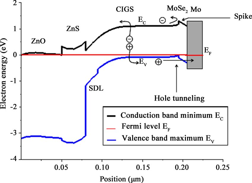
A. Sylla et al.

                                1. Introduction
                                High efficiency CIGS-based solar cells have been the focus of several years of
                                theoretical and experimental research. The recent high laboratory efficiency val-
                                ues of 22.9% and 23.4% (Solar Frontier) [1] [2] are close to the efficiency of 25%
                                achieved by crystalline silicon solar cells. These thin-film cells have achieved the
                                best performance of all second-generation cell technologies. The current
                                achieved efficiency is the result of the technological advances which allow the ef-
                                ficiency to be improved empirically by successive tests. In addition to the tech-
                                nological progress observed over the last two decades, significant efforts have
                                been devoted to understanding the physical properties of the key material of
                                these cells, namely the CIGS absorber layer. Indeed, the performance of these
                                cells largely depends on the physical properties of the CIGS alloys which are not
                                yet fully clarified. These include the nature and energy levels of the CIGS ab-
                                sorbing layer defects and the buffer/absorber interface defects [3] [4]. Moreover,
                                data about the material’s properties strongly depend on the used growth process
                                and characterization techniques [3] [4]. This entails input parameters of simula-
                                tion works may vary within wide ranges, imposing some limitation on the accu-
                                racy of simulated results. However, CIGS (namely CuIn1−xGaxSe2) material re-
                                mains one of the most promising semiconductor materials for photovoltaic
                                conversion based on polycrystalline thin-films because of several favorable
                                properties:
                                   1) Its bandgap can be varied continuously by changing the gallium content, x,
                                and its value is given by the commonly used formula (all bandgap energies in
                                eV) [5] [6] [7]:
                                                   EgCI1− x Gx S = (1 − x ) ⋅ EgCIS + x ⋅ EgCGS − b ⋅ x ⋅ (1 − x ) .

                                where b is the bowing parameter, EgCGS , EgCIS , the bandgaps of CGS and CIS
                                ternary compounds, respectively. Due to above-mentioned concerns, the value
                                of the bowing parameter can vary in the 0.15 - 0.24 eV range and that of EgCGS
                                and EgCIS in between 1.63 - 1.67 eV and 1.01 - 1.05 eV, respectively. We chose
                                here b = 0.21 eV, EgCGS = 1.65 eV and EgCIS = 1.04 eV [5]. All values are given
                                at 300˚K.
                                   2) The commonly referred surface defect layer (SDL), that is present between
                                the absorber and buffer layers increases the absorber bandgap at this interface by
                                lowering the valence band maximum with respect to the Fermi level, and hence
                                reduces the interface recombination rate. In fact, it has been found that this sur-
                                face defect layer is inverted to n-type such that the photogenerated electrons
                                pass through this region as majority carriers.
                                   3) CIGS is a direct bandgap alloy with an absorption coefficient that can reach
                                10 to 107 cm−1, here too depending on its fabrication process, so that a thin
                                   5

                                thickness of 0.5 μm is sufficient to absorb 90% of the incident photon flux [3].
                                   4) Unlike silicon, CIGS materials have exceptional tolerance to structural and
                                chemical defects
                                   On the other hand, the high cost and low abundance of indium and gallium

DOI: 10.4236/ojmsi.2021.94022                          340                            Open Journal of Modelling and Simulation
A. Sylla et al.
remains, in the long term, a major concern as well as the relatively significant
degradation of performance observed in case of long-term exposure to the at-
mosphere, which requires appropriate encapsulation. However, technological
progress has made it possible to produce cells with high efficiencies where the
usual CdS buffer layer is replaced by cheap and better eco-friendly materials as
ZnS, ZnO, and the ternary compound ZnO1−xSx. This latter is the most promis-
ing material with a variable bandgap from 3.6 eV to 3.2 eV [8] [9] [10].
Thin-film cells have nevertheless a small market share compared to their sili-
con counterparts but, in recent years, they have risen sharply mainly focusing on
their particular asset allowing the fabrication of flexible cells. Several routes have
been explored to fabricate them on metal and plastic foils jointly enhancing their
conversion efficiency by reducing sufficiently the photogenerated carrier recom-
bination caused by the bulk defects. The ultimate goal is affording the flexibility
with efficiencies and lifetime comparable to that of rigid cells.
One approach to decrease the raw material cost is to reduce drastically the
thickness of the absorber. In that case, the carrier photogeneration rate close to
the back contact can no more be negligible and the recombination rate at the
back interface is of prime importance. Another approach is to create an electric
field within the CIGS absorber by bandgap grading located at appropriate re-
gions. This results in various cell structures with different CIGS composition pro-
files: the so-called “front grading” which has a higher bandgap towards the buf-
fer layer, “back grading” which has a higher bandgap towards the back contact
layer and “double grading” which combines the two first profiles of grading. Thus,
front grading reduces recombination at the buffer/absorber junction and back
grading does close to the backside pushing back minority carriers towards the col-
lecting junction, then reducing carrier recombination at the absorber backside [11].
Many metals have been studied for contacting the photovoltaic cells to the ex-
ternal circuit. Mention may be made of molybdenum, chromium, tantalum,
manganese, gold and silver [12] [13]. Among those, the molybdenum is widely
used as back contact metal because of its relative stability at the high tempera-
tures that are encountered during CIGS deposition steps and its low contact re-
sistance with CIGS [14]. Its work function is about 4.53 eV [15]. In addition, the
existence of a thin MoSe2 layer at the CIGS/Mo interface has been clearly dem-
onstrated to improve the adhesion of CIGS to Mo as well as to enhance the effi-
ciency of the cell [14] [15] [16] [17]. MoSe2 is a semi-conductor material with a
bandgap of about 1.41 eV.
Lots of experimental studies have been carried out on the role of the MoSe2
layer at the interface of the CIGS/Mo contact of cells that use a CdS buffer to
achieve the p-n junction [18] [19] [20]. However, the formation of the thin MoSe2
layer depends on the fabrication process (deposition technique of CIGS, asso-
ciated temperatures…) that is used to realize the cell [18].
Several authors demonstrated the remarkable technological advantages of Mo.
But they also demonstrated the low reflexivity at the CIGS/Mo interface, which
DOI: 10.4236/ojmsi.2021.94022 341 Open Journal of Modelling and SimulationA. Sylla et al.
has a negative impact on the thin-film CIGS solar cells performance (reduction
of the short circuit current and the open circuit voltage). The aim of our work is
to determine the real contribution of the CIGS/Mo contact to the cell perfor-
mance through the MoSe2 thin layer presents at the CIGS/Mo interface. In this
paper, a ZnS buffer is used and we theoretically examine how the MoSe2 layer
influences the CIGS solar cell performance. For that purpose and after the opti-
mization of a MoSe2-free solar cell, we investigate successively the effects of the
CIGS and MoSe2 layer thickness and the barrier height of the Schottky MoSe2/Mo
back contact.
2. Numerical Simulation
In [3] [4], we reported the optimizing of CIGS-based solar cell including a MoSe2
layer at the CIGS/Mo interface. The values of front and back contact reflectivity
were set to 0% and the front and backside boundaries of the stacked semi-con-
ductors were described by the flat band metal/semi-conductor contact model.
Under those conditions, we demonstrated a maximum conversion efficiency of
26% [3].
Here, we use AFORS-HET to carry out the simulation work [21]. The simula-
tion of the MoSe2-free solar cell is based on Fermi level pinning model. The val-
ues of the optimized parameters are extracted from our previous papers [3] [4]
and take into account the Schottky barrier height at the back contact and the
reflectivity on the front (illuminated) side (Figure 1). The input parameters of
AFORS-HET simulation are listed in Table 1 and Table 2.
Figure 1. Schematic configuration of the optimized CIGS-based solar cell (a) with and (b)
without MoSe2 layer.
Table 1. Device properties: Subscripts n and p refer to electron and hole properties, re-
spectively, EB to majority carrier barrier height (EBn = EC − EF, EBp = EF − EV) and Sn,p to
back surface recombination velocity.
Front side Back side
EBn/EBp (eV) 0.02 0.3
Sn (cm/s)
107 107
Sp (cm/s)
Reflectivity (R) 5% 0%
DOI: 10.4236/ojmsi.2021.94022 342 Open Journal of Modelling and SimulationA. Sylla et al.
Table 2. Layer properties values used in AFORS-HET simulation: Sthn,p refers to carrier
thermal velocity, μn,p to carrier mobility, Eg to bandgap energy, NC/NV to effective density
of states in conduction and valence bands, (a)/(d) shallow acceptor and donor, and
ΔEC/ΔEV to band offset.
Layers properties
MoSe2 CIGSe ZnS ZnS i-ZnO ZnO:Al
Thickness (μm) 0.01 variable 0.015 0.03 0.02 0.03
Band gap Eg (eV) 1.41 1.19 1.34 3.6 3.2 3.2
Electron affinity χ (eV) 4.4 4.5 4.5 4.15 4.5 4.5
Dielectric constant εr 14.9 13.6 13.6 9 9 9
NC (cm−3) 2.2 × 10¹⁸ 6.8 × 10¹⁷ 6.8 × 10¹⁷ 2.2 × 10¹⁸ 3 × 10¹⁸ 3 × 10¹⁷
NV (cm−3) 1.8 × 10¹⁸ 1.5 × 10¹⁹ 1.5 × 10¹⁹ 1.8 × 10¹⁹ 1.7 × 10¹⁹ 1.7 × 10¹⁹
Sthn , Sthp (cm/s) 107
μn (cm2/Vs) 100 100 10 100 100 100
μp (cm /Vs)
2
50 50 1.25 25 31 31
Doping level (cm ) −3
10 (a)
19
6 × 10 (a) 6 × 10 (a)
17 17
10 (d)
18
10 (d)
18
10 (d)
20
MoSe2/CIGS CIGS/SDL SDL(CIGS)/ZnS ZnS/i-ZnO
ΔEC (eV) 0.1 0 0.35 (0.35) −0.35
ΔEV (eV) −0.12 −0.15 −1.19 (−2.06) 0.05
Contrary to our previously reported simulation, the reflectivity at front side is
R = 5% and the back Schottky barrier height EB = 0.3 eV is higher than that pre-
viously used (EB ≈ 0.02 eV) [3] [4]. The Schottky barrier height is deduced from
the formula EB = χ + Eg − ΦMo where χ and Eg denote respectively the electronic
affinity and the bandgap of the semi-conductor material in contact with Mo and
ΦMo the work function of molybdenum. AFORS-HET uses the Shockley-Read-
Hall recombination model and solves the fundamental one-dimensional semi-
conductor equations for steady-state equilibrium conditions under solar illumi-
nation [21]. The metal-semiconductor contact simulation is implemented ac-
cording to the metal work function. Therefore, the contact can operate either in
flat band mode or in band bending mode. AFORS-HET simulator allows the
calculation of basic characteristics such as band diagram, generation and recom-
bination rates, carrier densities and cell currents [21].
The simulated cell structures consist of six or seven stacked layers, depending
the p-MoSe2 layer is absent or present, respectively (see Figure 1). These layers
are deposited on a soda lime glass (SLG) substrate. Only the front contact boun-
daries of the solar cells are described by the flat band metal/semiconductor con-
tact model. The solar cell front side is illuminated under AM1.5G solar spectrum
corresponding to an incident power density of 100 mW/cm2 at room tempera-
ture (1 Sun). Under these conditions, we calculated the effects of the thickness of
the CIGS and MoSe2 layers that varied from 0.1 μm to 10 μm and from 10 nm to
100 nm respectively. As for the Schottky barrier height at the back MoSe2/Mo
contact it has been varied from 0.2 eV to 0.65 eV according to the work function
DOI: 10.4236/ojmsi.2021.94022 343 Open Journal of Modelling and SimulationA. Sylla et al.
of molybdenum that was tuned from 5.16 eV to 5.61 eV.
3. Results and Discussion
3.1. Solar Cell Optimization
The thickness of each layers of the solar cells, including or not the MoSe2 layer, has
been optimized. The conversion efficiency obtained for the MoSe2-free solar cell η =
24.6% is equal to that of the cell including a MoSe2 thin-film layer at the CIGS/Mo
contact interface. This value of efficiency has been obtained for a 3 μm-thick CIGS
absorber with a front side reflectivity of 5%. The Schottky barrier height is 0.3 eV
and 0.18 eV for the solar cells with and without MoSe2 layer respectively.
The mechanism of carrier transport in metal/semi-conductor contact is inti-
mately related to the energy band structure at the interface under thermodynamic
equilibrium conditions. We therefore examined in the next paragraphs the real
electrical impact of the MoSe2/Mo contact on CIGS solar cell performance. Our
approach consisted in modifying the Schottky barrier height at the interface of
CIGS/Mo and MoSe2/Mo intimate contacts of the two cells structure and varying
the MoSe2 and CIGS layers thickness, the other parameters being kept constant.
3.2. Effect of the MoSe2 Layer Thickness on Internal
Quantum Efficiency (IQE)
To analyze the effect of the MoSe2 layer thickness on the IQE (or η), we varied its
value from 10 to 100 nm (Figure 2). We can see that for MoSe2 layer thickness
larger than 30 nm the cell efficiency remains almost constant. So, the MoSe2
layer thickness was set at 30 nm for the other studies. The photocarrier recom-
bonation is considerable at the CIGS/Mo contact interface. The presence of the
MoSe2 layer with a relatively large thickness (30 nm) moves this zone of recom-
bination away from the CIGS absorber layer. Under these conditions the tunnel
effet outweighs the recombination and improves the efficiency.
3.3. Effect of the MoSe2 Layer on the External
Quantum Efficiency (EQE)
The EQE expresses the flow of electrons through the external circuit of use
Figure 2. Effect of the MoSe2 layer thickness on the cell efficiency (absorbing layer thick-
ness is of 3 μm).
DOI: 10.4236/ojmsi.2021.94022 344 Open Journal of Modelling and SimulationA. Sylla et al.
according to the wavelength absorbed. Compared to IQE, it takes into account
two important factors that are optical losses and photocarrier recombinations.
For the large absorber thicknesses (tCIGS ≥ 3 μm), the EQE is almost identical for
both structures, with and without MoSe2 layer. On the other hand, for CIGS
thicknesses less than 3 μm, the EQE of the solar cell with a MoSe2 layer is higher.
We have plotted the EQE curves for a solar cell including a 1.5 μm thick CIGS
absorbing layer with and without the MoSe2 layer (30 nm thick). Figure 3 shows
that the cell including the MoSe2 layer offers a higher EQE value in the long wa-
velength range compared to the MoSe2-free cell.
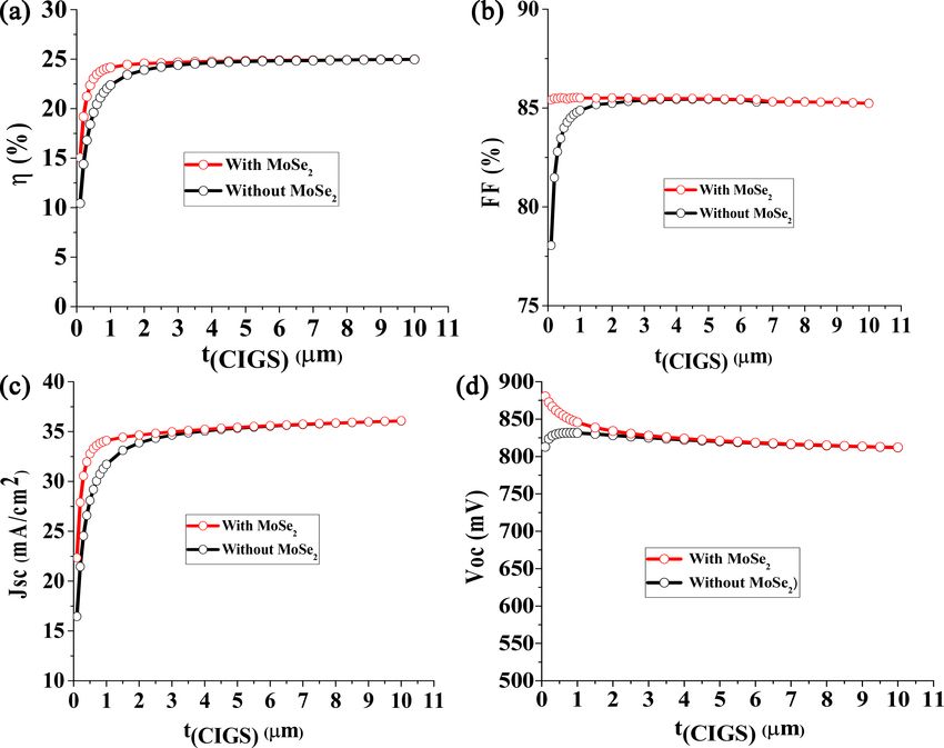
3.4. Effet of CIGS Layer Thickness on the Electrical Parameters
In order to investigate the effect of the absorber layer thickness on the electrical
parameters of cells with and without a MoSe2 layer, we varied the CIGS thick-
ness from 0.1 to 10 μm. The photovoltaic performance of cells including a MoSe2
layer are better than that of the MoSe2-free solar cell (Figure 4) But this en-
hancement only appears for absorber thickness less than 3.5 μm, that is at least
the majority, if not all, of experimental cases. For higher thickness values the
performance of the two kinds of cells are almost identical: the efficiency increas-
es up to about 25% with a slope of around 0.1% per additional micron of layer
thickness (Figure 4(a)). It can also be observed that the efficiency of the cell
with a MoSe2/Mo back contact remains almost constant, about 24.6% down to
an absorber layer thickness of 1.5 μm, while that of the MoSe2-free cell decreases
from 24.6% to 23.4% in the same range. So, the efficiency of the cell with a MoSe2
layer is more independent on the absorbing layer thickness since it starts to de-
crease when CIGS thickness is less than 1.5 μm, while that of the MoSe2-free cell
starts to decrease at approximately 3.5 μm. For CIGS layer thickness less than
approximately 0.5 μm, the effciency decreases rapidly in both cases because the
carrier generation occurs very close to the back side where the carrier recombi-
nation is considerable. It can be seen in Figure 4(d) that the short circuit current
presents a similar evolution than efficiency over the whole range of the absorber
thickness variation. Looking now at FF in Figure 4(b), we observe that the fill
factor of the cell with MoSe2 layer remains almost unchanged, whatever the
Figure 3. Effect of MoSe2 layer (30 nm thick) on the EQE (absorber thickness is of 1.5
μm).
DOI: 10.4236/ojmsi.2021.94022 345 Open Journal of Modelling and SimulationA. Sylla et al.
Figure 4. Effects of absorber layer thickness on cell performance for cell with and without
MoSe2 layer (30 nm thick). (a) conversion efficiency η, (b) fill factor FF, (c) open circuit
volatge VOC and (d) short circuit current JSC.
thickness of the absorber is. On the over hand, for the MoSe2-free solar cell, the fill
factor starts decreasing at a switchover point of 3.5 μm. A similar evolution of the
open circuit voltage is observed for absorber layer thickness higher than 3.5 μm.
For the solar cell including the MoSe2 layer, an increase of the open circuit voltage
is observed for lowest thickness values of the CIGS absorbing layer (Figure 4(c),
tCIGS < 3.5 μm) since it is almost the reverse case for the MoSe2-free cell.
To get a deeper insight into the better performance of the thinner CIGS solar
cell with a MoSe2/Mo layer, we analysed more deeply the band structure (Figure
5). Under maximum effciency conditions, i.e. the work function of Mo, p-CIGS
and p+-MoSe2 are eφMo = 5.51 eV, eφSC1 = 5.61 eV and eφSC2 = 5.8 eV, respectively
(other values of parameters are that of Figure 1), eφSC1 and eφSC2 always remain
greater than eφMo and the CIGS/Mo and MoSe2/Mo intimate contacts are of
Schottky-type. However, unlike the MoSe2-free cell, the highly p-doped MoSe2
layer improves the majority carrier flow at the CIGS/Mo interface by tunneling
effect. This tunnel barrier effect changes the intimate CIGS/Mo contact from
Schottky type to quasi-ohmic type. Therefore the MoSe2 layer has the ability to
improve the generated carrier collection and increase the open circuit voltage
and the conversion efficiency. In fact, the MoSe2 layer has a wider gap than that
of the absorber, then creating a back electric field that considerably reduces re-
combination at the CIGS back side. Furthermore, at the CIGS/MoSe2 interface
the conduction band also exhibits a spike that contributes to the reduction of the
CIGS back surface recombination losses by reflecting the photogenerated elec-
trons back to the junction where they are collected efficiently.
DOI: 10.4236/ojmsi.2021.94022 346 Open Journal of Modelling and SimulationA. Sylla et al.
3.5. Effet of Schottky Barrier Height at the Back Contact Interface
To investigate the effect of the Schottky barrier height at the CIGS/Mo contact
interface, we varied the metal work function from 5.16 to 5.61 eV for MoSe2-free
and MoSe2/Mo contacts (Figure 6). As far as the metal work function ΦMo ≥ 5.36
eV, i.e. the Schottky barrier height is less than 0.45 eV (work function of
p+-MoSe2, eφSC2, is 5.8 eV), the electrical characteristics (efficiency, fill factor,
Figure 5. Calculated band structure of the CIGS solar cell with additional MoSe2 layer
under zero-bias voltage.
Figure 6. Effects of the Schottky barrier height on cell performance for MoSe2-free cell
and cell with additional MoSe2 layer. (a) conversion efficiency η, (b) fill factor FF, (c)
open circuit volatge VOC and (d) short circuit current JSC. (absorbing layer thickness is 1.5
μm).
DOI: 10.4236/ojmsi.2021.94022 347 Open Journal of Modelling and SimulationA. Sylla et al.
open circuit voltage) of the cell with a MoSe2 tunnel layer are better than those of
the MoSe2-free cell. However, related values increase slightly with the increase of
the metal work function value. Whatever ΦMo value is, the short circuit current is
higher for the MoSe2 cell. In fact, the MoSe2 tunnel layer eliminates the blocking
effect of the Schottky barrier height to the flow of holes. In contrast, for ΦMo ≤
5.36 eV, the barrier height becomes prohibitive (EB ≥ 0.45 eV) and a pronounced
degradation of the conversion efficiency, open circuit voltage and fill factor val-
ues is observed. They are then below that of a MoSe2-free cell. For the investi-
gated metal work function range, the barrier height at the intimate CIGS/Mo
contact interface is relatively low and decreases from 0.53 to 0.08 eV. In this
range of barrier height values, each of them is related to a metal work function
value via the formula of Section II. So, the decrease of the barrier height from
0.53 eV to 0.08 eV corresponds to an increase of the metal work function value
from 5.16 eV to 5.61 eV. The performance of the MoSe2-free cell remains low
but almost constant and the negative effect of the Schottky barrier height is only
observed for values greater than 0.43 eV. In conclusion, it is the quasi-ohmic
nature of the MoSe2/Mo contact and the reduction of the CIGS back surface re-
combination rate that increase the open circuit voltage, the fill factor and the
conversion efficiency as it has been demonstrated by other authors [18] [20].
4. Conclusions
This article focused on the comparative theoretical study, using AFORS-HET
software, of two kinds of CIGS-based solar cells performance differentiating by
the presence of a MoSe2 layer at the CIGS/Mo interface. Overall conclusion is
that the performance of a cell including such a MoSe2 layer is better than that of
the MoSe2-free cell. Its thickness does not seem to be very challenging; 30 nm
can be a suitable value. The MoSe2 layer, firstly, acts as a tunneling barrier pro-
viding a quasi-ohmic back contact behavior and, secondly, creates a back surface
electric field owing to its wider bandgap than that of CIGS absorber. However,
to achieve such a behavior, the molybdenum work function shall be higher than
5.36 eV. These improvements are valid only for absorbing layer thickness less
than 3.5 μm that constitute all practical cases, though. Moreover, the MoSe2 layer
beneficial effect is all the more important as the absorbing layer is thin, especial-
ly below 1 μm. Under those conditions, cells including a MoSe2 tunnel layer can
theoretically exhibit an efficiency of about 24.6%.
The model studied in this work has two junctions: the n-Zn (O, S)/n-SDL iso-
type heterojunction and the n-SDL/p-CIGS homojunction buried in the CIGS ab-
sorber layer (buried junction). Under these conditions, the n-Zn (O, S)/p-CIGS
heterojunction raises several questions, in particular the advantage of the buffer
which does not really form the collecting junction with the CIGS absorber layer,
the density and the influence of defects at the interface of the homo- and hete-
rojunction as well as the maximum efficiency achievable. In perspective, we plan
to study the doping model where the surface defect layer (SDL) of the CIGS ab-
DOI: 10.4236/ojmsi.2021.94022 348 Open Journal of Modelling and SimulationA. Sylla et al.
sorber is considered to be a chalcopyrite-like n-doped material with a bandgap
higher than that of CIGS. These calculations could be carried out with the SCAPS-
1D software package widely used for the simulation of CIGS-based heterojunc-
tions.
Conflicts of Interest
The authors declare no conflicts of interest regarding the publication of this pa-
per.
References
[1] Nakamura, M., Yamaguchi, K., Kimoto, Y., Yasaki, Y., Kato, T. and Sugimoto, H.
(2019) Cd-Free Cu(In,Ga)(Se,S)2 Thin-Film Solar Cell with Record Efficiency of
23.35%. IEEE Journal of Photovoltaics, 9, 1863-1867.
https://doi.org/10.1109/JPHOTOV.2019.2937218
[2] Aboulfadl, H., Keller, J., Larsen, J., Thuvander, M., Riekehr, L., Edoff, M. and Platz-
er-Björkman, C. (2019) Microstructural Characterization of Sulfurization Effects in
Cu(In,Ga)Se2 Thin Film Solar Cells. Microscopy and Microanalysis, 25, 532-538.
https://doi.org/10.1017/S1431927619000151
[3] Sylla, A., Touré, S. and Vilcot, J.-P. (2017) Numerical Modeling and Simulation of
CIGS-Based Solar Cells with ZnS Buffer Layer. Open Journal of Modelling and Si-
mulation, 5, 218-231. https://doi.org/10.4236/ojmsi.2017.54016
[4] Sylla, A., Touré, S. and Vilcot, J.-P. (2017) Theoretical Analysis of the Effects of
Band Gaps and the Conduction Band Offset of ZnS-CIGS Layers, as Well as Defect
Layer Thickness. International Journal of Science and Research, 6, 855-861.
https://www.ijsr.net/search_index_results_paperid.php?id=ART20178061
[5] Wei, S.-H., Zhang, S.B. and Zunger, A. (1998) Effects of Ga Addition to CuInSe2 on
Its Electronic, Structural, and Defect Properties. Applied Physics Letters, 72,
3199-3201. https://doi.org/10.1063/1.121548
[6] Wei, S.-H. and Zunger, A. (1995) Band Offsets and Optical Bowings of Chalcopy-
rites and Zn-Based II-VI Alloys. Journal of Applied Physics, 78, 3846-3856.
https://doi.org/10.1063/1.359901
[7] Mudryi, A.V., Gremenok, V.F., Karotki, A.V., Zalesski, V.B., Yakushev, M.V.,
Luckert, F. and Martin, R. (2010) Structural and Optical Properties of Thin Films of
Cu(In,Ga)Se2 Semiconductor Compounds. Journal of Applied Spectroscopy, 77,
371-377. https://doi.org/10.1007/s10812-010-9341-5
[8] Ahn, B.T., Larina, L., Kim, K.H. and Ahn, S.J. (2008) Development of New Buffer
Layers for Cu(In,Ga)Se2 Solar Cells. Pure and Applied Chemistry, 80, 2091-2102.
https://doi.org/10.1351/pac200880102091
[9] Pettersson, J. (2012) Modeling Band Gap Gradients and Cd-Free Buffer Layers in
Cu(In,Ga)Se2 Solar Cells. Ph.D. Thesis, Uppsala University, Uppsala.
https://www.diva-portal.org/smash/get/diva2:501452/FULLTEXT01.pdf
[10] Meyer, B.K., Polity, A., Farangis, B., He, Y., Hasselkamp, D., Krämer, T. and Wang,
C. (2004) Structural Properties and Band Gap Bowing of ZnO1−xSx Thin Films De-
posited by Reactive Sputtering. Applied Physics Letters, 85, 4929-4931.
https://doi.org/10.1063/1.1825053
[11] Decocka, K., Lauwaerta, J. and Burgelmana, M. (2010) Characterization of Graded
CIGS Solar Cells. Energy Procedia, 2, 49-54.
DOI: 10.4236/ojmsi.2021.94022 349 Open Journal of Modelling and SimulationA. Sylla et al.
https://doi.org/10.1016/j.egypro.2010.07.009
[12] Orgassa, K., Schock, H.W. and Werner, J.H. (2003) Alternative Back Contact Mate-
rials for Thin-Film Cu(In,Ga)Se Solar Cells. Thin Solid Films, 431-432, 387-391.
https://doi.org/10.1016/S0040-6090(03)00257-8
[13] Matson, R.J., Jamjoum, O., Buonaquisti, A.D., Russell, P.E., Kazmerski, L.L., Shel-
don, P. and Ahrenkiel, R.K. (1984) Metal Contacts to CuInSe2. Solar Cells, 11, 301-305.
https://doi.org/10.1016/0379-6787(84)90019-X
[14] Assmann, L., Bernède, J.C., Drici, A., Amory, C., Halgand, E. and Morsli, M. (2005)
Study of the Mo Thin Films and Mo/CIGS Interface Properties. Applied Surface
Science, 246, 159-166. https://doi.org/10.1016/j.apsusc.2004.11.020
[15] Lide, D.R. (2005) CRC Handbook of Chemistry and Physics. Internet Version, CRC
Press, Boca Raton, 2208. http://www.hbcpnetbase.com
[16] Klinkert, T., Theys, B., Patriarche, G., Jubault, M., Donsanti, F., Guillemoles, J.-F.
and Lincot, D. (2016) New Insights into the Mo/Cu(In,Ga)Se2 Interface in Thin Film
Solar Cells: Formation and Properties of the MoSe2 Interfacial Layer. The Journal of
Chemical Physics, 145, Article ID: 154702. https://doi.org/10.1063/1.4964677
[17] Kohara, N., Nishiwaki, S., Hashimoto, Y., Negami, T. and Wada, T. (2001) Electric-
al Properties of the Cu(In,Ga)Se2/MoSe2/Mo Structure. Solar Energy Materials &
Solar Cells, 67, 209-215. https://doi.org/10.1016/S0927-0248(00)00283-X
[18] Hsiao, K.-J., Liu, J.-D., Hsieh, H.-H. and Jiang, T.-S. (2013) Electrical Impact of
MoSe2 on CIGS Thin-Film Solar Cells. Physical Chemistry Chemical Physics, 41,
18174-18178. https://doi.org/10.1039/c3cp53310g
[19] Wada, T., Kohara, N., Nishiwaki, S. and Negami, T. (2001) Characterization of the
Cu(In,Ga)Se2/Mo interface in CIGS. Thin Solid Films, 387, 118-122.
https://doi.org/10.1016/S0040-6090(00)01846-0
[20] Zhang, X., Kobayashi, M. and Yamada, A. (2017) Comparison of Ag(In,Ga)Se2/Mo
and Cu(In,Ga)Se2/Mo interfaces in solar cells. ACS Applied Materials & Interfaces,
9, 16215-16220. https://doi.org/10.1021/acsami.7b02548
[21] Varache, R., Leendertz, C., Gueunier-Farret, M.E., Haschke, J., Muñoz, D. and Korte,
L. (2015) Investigation of Selective Junctions Using a Newly Developed Tunnel Cur-
rent Model for Solar Cell Applications. Solar Energy Materials & Solar Cells, 141,
14-23. https://doi.org/10.1016/j.solmat.2015.05.014
DOI: 10.4236/ojmsi.2021.94022 350 Open Journal of Modelling and SimulationYou can also read