Improvement in Light Output of Ultraviolet Light-Emitting Diodes with Patterned Double-Layer ITO by Laser Direct Writing - MDPI
←
→
Page content transcription
If your browser does not render page correctly, please read the page content below
nanomaterials

Article
Improvement in Light Output of Ultraviolet
Light-Emitting Diodes with Patterned Double-Layer
ITO by Laser Direct Writing
Jie Zhao 1,2 , Xinghuo Ding 1,2 , Jiahao Miao 1,2 , Jinfeng Hu 1,2 , Hui Wan 1,2
and Shengjun Zhou 1,2,3, *
 1   Key Laboratory of Hydraulic Machinery Transients (Wuhan University), Ministry of Education,
     Wuhan 430072, China; zjie1994@whu.edu.cn (J.Z.); xinghuo@whu.edu.cn (X.D.); miaojh@whu.edu.cn (J.M.);
     2017282080101@whu.edu.cn (J.H.); wanhui_hb@whu.edu.cn (H.W.)
 2   Center for Photonics and Semiconductors, School of Power and Mechanical Engineering, Wuhan University,
     Wuhan 430072, China
 3   State Key Laboratory of Applied Optics, Changchun Institute of Optics, Fine Mechanics and Physics,
     Chinese Academy of Sciences, Changchun 130033, China
 *   Correspondence: zhousj@whu.edu.cn; Tel.: +86-027-5085-3293

 Received: 7 January 2019; Accepted: 30 January 2019; Published: 4 February 2019

 Abstract: A patterned double-layer indium-tin oxide (ITO), including the first unpatterned ITO
 layer serving as current spreading and the second patterned ITO layer serving as light extracting,
 was applied to obtain uniform current spreading and high light extraction efficiency (LEE)
 of GaN-based ultraviolet (UV) light-emitting diodes (LEDs). Periodic pinhole patterns were formed
 on the second ITO layer by laser direct writing to increase the LEE of UV LED. Effects of interval of
 pinhole patterns on optical and electrical properties of UV LED with patterned double-layer ITO
 were studied by numerical simulations and experimental investigations. Due to scattering out of
 waveguided light trapped inside the GaN film, LEE of UV LED with patterned double-layer ITO
 was improved as compared to UV LED with planar double-layer ITO. As interval of pinhole patterns
 decreased, the light output power (LOP) of UV LED with patterned double-layer ITO increased.
 In addition, UV LED with patterned double-layer ITO exhibited a slight degradation of current
 spreading as compared to the UV LED with a planar double-layer ITO. The forward voltage of UV
 LED with patterned double-layer ITO increased as the interval of pinhole patterns decreased.

 Keywords: UV LEDs; double-layer ITO; pinhole pattern; current spreading; light output power

1. Introduction
     Ultraviolet (UV) light-emitting diodes (LEDs) have attracted considerable attention due to their
potential applications in sterilization, water purification, photocatalyst, and solid-state lighting [1–8].
The improvement of light output is crucial for the realization of high-efficiency UV LEDs.
The uniform current spreading is strongly correlated with light output and device reliability [9–12].
Thus, p-type electrodes possessing low contact resistivity as well as high transmittance have been
extensively studied. Several kinds of transparent conductive layer such as metal nanowires [13–16],
graphene [17–19], carbon nanotubes [20,21], and conductive polymers [22–24] have been reported to
improve the current spreading of LEDs. For top-emitting LEDs, indium-tin-oxide (ITO) has been widely
used to increase current spreading uniformity over the entire active region due to its high optical
transmittance and excellent electrical conductivity [25–27]. In addition, thermal annealing process
has been used to improve ohmic contact performance between ITO and p-GaN [28,29]. However, the ITO
exhibits optical degradation at UV wavelength region during the thermal annealing process [30].

Nanomaterials 2019, 9, 203; doi:10.3390/nano9020203                      www.mdpi.com/journal/nanomaterials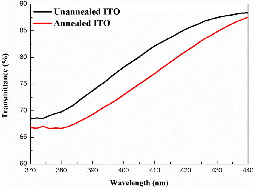
Nanomaterials 2019, 9, 203                                                                                      2 of 9

     On the other hand, the light extraction efficiency (LEE) is limited by total internal reflection (TIR)
because of large difference in refractive index between sapphire substrate, GaN film, ITO and the air.
To overcome TIR at the ITO-air interface, microstructures formed on ITO have been reported to redirect
the orientation of photons to favor emission into the air, leading to increasing scattering probability of
photons at the ITO-air interface [31–37]. Moreover, compared to randomly distributed ITO pattern,
the escape probability of photons emitting from the active region can be further increased by a regularly
distributed ITO pattern [38]. However, patterned ITO has been shown to degrade the current spreading
performance of UV LED due to an increase in sheet resistance [39–41]. Adding an annealed bottom
ITO layer is an effective way to stabilize the current spreading and prevent electrical degradation.
     In this study, we combined two single ITO layers into double-layer ITO to obtain excellent ohmic
contact and high LEE. The first ITO layer was annealed to form low-resistance ohmic contact with
p-GaN. The unannealed second ITO layer was patterned to increase the scattering probability of
photons at the ITO-air interface. The periodic pinhole patterns with different intervals were fabricated
on the unannealed second ITO layer using laser direct writing. Effects of interval of pinhole patterns
on the optical and electrical characteristics of UV LED with patterned double-layer ITO were studied
in detail using numerical simulations and experimental investigations.

2. Materials and Methods
      The GaN-based UV LED was grown on patterned sapphire substrate (PSS) with a sputtered AlN
nucleation layer (15 nm) using the metal-organic chemical vapor deposition (MOCVD) technique.
Trimethylgallium (TMGa), trimethylindium (TMIn), trimethylaluminum (TMAl), and ammonia (NH3 )
were used as precursors of Ga, In, Al, and N, respectively. Silane (SiH4 ) and bis (cyclopentadienyl)
magnesium (Cp2 Mg) were used as the n- and p-dopant sources, respectively. The epitaxial structure
of UV LED includes a 15-nm-thick sputtered AlN nucleation layer, a 2.5-µm-thick undoped GaN
layer, a 2-µm-thick n-GaN layer, a 12-pair In0.02 Ga0.98 N (2.1 nm)/GaN (2.3 nm) superlattice layer
(SL), a 15-pair In0.07 Ga0.93 N (3 nm)/GaN (12 nm) multiple quantum well (MQW) active layer,
a 28-nm-thick p-InGaN layer, a 5-pair p-Al0.2 Ga0.8 N (1 nm)/GaN(2 nm) SL, a 50-nm-thick p-GaN
layer, and a 10-nm-thick p+ -GaN layer. The peak emission wavelength of UV LED is 375 nm.
Figure 1a shows a schematic representation of the 375 nm UV LED epitaxial structure. Figure 1b shows
the cross-sectional transmission electron microscope (TEM) image of the UV LED epitaxial structure
grown on PSS. Figure 1c shows the magnified cross-sectional TEM image of In0.02 Ga0.98 N/GaN SL,
In0.07 Ga0.93 N/GaN MQW, p-InGaN layer, and p-Al0.2 Ga0.8 N /GaN SL.

      Figure 1. (a) Schematic representation of the UV LED epitaxial structure; (b) cross-sectional TEM image
      of the UV LED epitaxial structure; (c) magnified cross-sectional TEM image showing In0.02 Ga0.98 N/GaN
      SL, In0.07 Ga0.93 N/GaN MQW, and p-Al0.2 Ga0.8 N /GaN SL.

    UV LEDs with a patterned double-layer ITO were fabricated. The detailed fabrication process is
composed of the following steps. Firstly, inductively coupled plasma (ICP) etching based on BCl3 /Cl2
mixture gas was used to form GaN mesa by removing a portion of p-GaN layer and MQW active layer
Nanomaterials 2019, 9, 203                                                                            3 of 9

to expose the n-GaN layer (Step (1)). Then, the first 30-nm-thick ITO layer was subsequently deposited
on the p-GaN layer using an electron beam evaporator, followed by thermal annealing in N2 ambient
at 540 ◦ C for 20 min to obtain good ohmic contact with p-GaN (Step (2)). Next, the second 120-nm-thick
ITO layer was deposited on the first ITO layer, and the periodic pinhole patterns were then formed on
the second ITO layer by laser direct writing (Step (3)). Finger-like Cr/Pt/Au (30 nm/30 nm/2000 nm)
multilayers were adopted for both n-electrode and p-electrodes. The Cr/Pt/Au multilayers were
deposited on the second patterned ITO layer for the formation of p-electrode. Meanwhile, the same
Cr/Pt/Au multilayers were also deposited on the exposed n-GaN layer for the formation of
the n-electrode (Step (4)). Finally, the UV LED wafers were thinned down to about 120 µm and diced
into chips with dimension of 1132 × 1132 µm2 (Step (5)). Except for different interval of pinhole
patterns fabricated on the second ITO layer, the fabrication process of these UV LEDs is identical.
The diameters of pinhole patterns were 2 µm in UV LED II, UV LED III, and UV LED IV, while intervals
of pinhole patterns were 400 nm, 600 nm, and 800 nm, respectively. For comparison, the UV LED I
with planar double-layer ITO was also prepared. The light output power (LOP)-current-voltage
(L-I-V) characteristics of UV LEDs were measured using an integrating sphere and a semiconductor
parameter analyzer (Keysight B2901A). Figure 2a shows a schematic representation of the UV LED with
a patterned double-layer ITO. Figure 2b shows a cross-sectional schematic representation of the UV
LED with a patterned double-layer ITO. Figure 2c shows the top-view scanning electron microscopy
(SEM) image of the fabricated UV LED chip.

      Figure 2. (a) Schematic representation of the UV LED with a patterned double-layer ITO;
      (b) cross-sectional schematic representation of the UV LED with a patterned double-layer ITO;
      (c) top-view SEM image of the fabricated UV LED chip.

     Figure 3 shows an energy band diagram of the UV LED at forward bias. When a current is passed
through the UV LED, electrons and holes are injected into the In0.07 Ga0.93 N/GaN MQW active layer from
the n-type GaN and p-type GaN layers, respectively. The electrons and holes recombine radiatively in
the In0.07 Ga0.93 N/GaN MQW active layer, thereby emitting photons of light, as shown in Figure 3.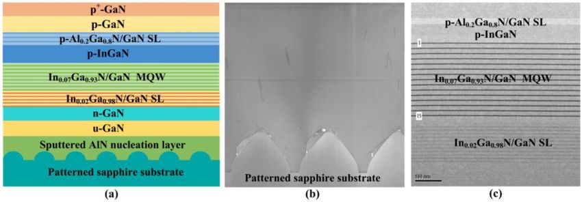
Nanomaterials 2019, 9, 203 4 of 9
Figure 3. Energy band diagram of the UV LED at forward bias.
3. Results and Discussion
The pinhole patterns on the second ITO layer were fabricated by laser direct writing system
(4PICO.BV, Netherlands). First, the photoresist (ma-p1275HV) was spin-coated on GaN-based
wafer at 4000 rpm for 60 s. Then, laser direct writing was performed on the photoresist film to
obtain pinhole patterns, which will be transferred to the ITO film. The irradiating red laser beam
(λ = 635 nm) was focused onto the surface of spin-coated photoresist through a dedicated objective lens
(numerical aperture (NA) = 0.85, focal length = 0.6 mm, and magnification = 100×) to correct for surface
errors. Then an ultraviolet laser beam (λ = 405 nm) was normally directed to the surface of photoresist with
a spot diameter of 300 nm and an energy density of 60 mJ/cm2 through the same objective lens. The laser
beam was scanned on the photoresist with a scan speed of 200 mm/s and stepping distance of 150 nm
by a motorized stage. The wafer was then submersed into developer (ma-D 331) for 70 s to remove
the area that has been exposed. Finally, pinhole patterns were transferred from photoresist onto the second
ITO layer by wet chemical etching process. Figure 4 shows top-view SEM images of the pinhole patterns
with different intervals. The diameter and intervals of the pinhole patterns of UV LED II, UV LED III,
and UV LED IV were 2 µm/400 nm, 2 µm/600 nm, and 2 µm/800 nm, respectively.
Figure 4. Top-view SEM images of the pinhole patterns with different intervals: (a) 400 nm; (b) 600 nm;
(c) 800 nm.
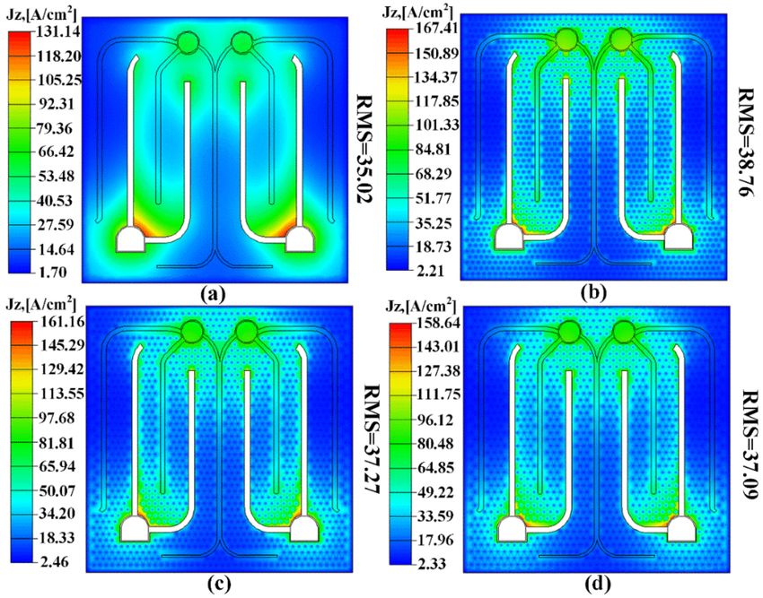
We measured transmittance spectra of the evaporated ITO films before and after thermal
annealing. Figure 5 shows the transmittance spectra of unannealed ITO and annealed ITO films
in the wavelength range of 370–440 nm measured by a UV/VIS/NIR spectrometer. The transmittance
of the unannealed ITO and annealed ITO were 68.81% and 66.88% at 375 nm, respectively.
The transmittance of the unannealed ITO was 2.89% higher than that of the annealed ITO.
It was indicated that the transmittance of ITO exhibited optical degradation at UV wavelength region
after thermal annealing, which would lead to a decrease in LEE of UV LED. To avoid the decrease
in transmittance of ITO at the UV wavelength region, the second ITO layer remains unannealed in
Nanomaterials 2019, 9, 203                                                                                  5 of 9

our design. In addition, a combined method including electron beam evaporation and subsequent
magnetron sputtering can further improve the optical transmittance of ITO [42].

      Figure 5. Transmission spectra of the unannealed ITO and annealed ITO films in the wavelength range
      of 370–440 nm.

     We investigated the effect of interval of pinhole patterns on current spreading of UV LED with
double-layer ITO using SimuLED commercial software package. Figure 6 shows simulation results
of the current density distribution of UV LED I, UV LED II, UV LED III, and UV LED IV at 350 mA.
The root mean square (RMS) of current density in the active region of UV LED I, UV LED II, UV LED III,
and UV LED IV was 35.02 A/cm2 , 38.76 A/cm2 , 37.27 A/cm2 , and 37.09 A/cm2 , respectively.
Compared with UV LED I, the RMS of current density in the active region of UV LED with patterned
double-layer ITO was slightly increased. Meanwhile, the RMS of current density in the active region
of UV LEDs increased with decreasing interval of the pinhole patterns on the second ITO layer.
The slightly increased RMS of current density resulted from non-uniform current spreading.

      Figure 6. SimuLED simulation of the current density distribution in the active region of UV LED
      at 350 mA: (a) UV LED I; (b) UV LED II; (c) UV LED III; (d) UV LED IV.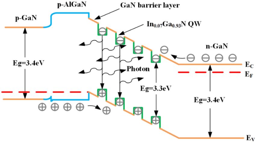
Nanomaterials 2019, 9, 203                                                                               6 of 9

      The Finite-Difference Time-Domain (FDTD) method was applied for numerical simulation to
clarify the effect of interval of pinhole patterns on the LEE of UV LED. To save computational memory
and simulation time, the thickness of the sapphire substrate was fixed at 1 µm. Other structure
parameters in the simulation were similar with the actual LED structure. The simplified UV LED
structure model was depicted in Figure 7. The boundary conditions were a perfectly matched layer
(PML) on top of the simulation region. The PML boundary absorbs incident light with zero reflection.
Reflective metal boundaries were used at the bottom and four broad sidewalls. The top monitor
was located 800 nm above the surface of the second patterned ITO to receive the optical waves
extracted to air and calculate the LEE of the UV LED.
      In order to present the random propagation of unpolarized photons within the active region,
sufficient dipole sources with wavelength of 375 nm were regularly distributed throughout the middle
of the MQW layer with an interval of 1 µm. Three orientations of dipole sources were along the x-, y-,
and z-axis. Compared to UV LED I, the LEEs of UV LED II, UV LED III, and UV LED IV were improved
by 13.06%, 12.04%, and 7.02%, respectively. The enhancement in LEE was attributed to the formation
of pinhole patterns on the second ITO layer, which redirected the photon propagation into the air
escape cone and provided the photons with multiple opportunities to escape from the LED surface.

      Figure 7. Schematic illustration of the FDTD simulation model for UV LED with a patterned double
      layer ITO.

      The LOPs of UV LEDs versus injection current were shown in Figure 8a. At an injection current
of 350 mA, the LOPs of UV LED I, UV LED II, UV LED III, and UV LED IV were 32.60 mW, 36.70 mW,
36.38 mW, and 34.75 mW, respectively. Compared with UV LED I, the LOPs of UV LED II, UV LED III,
and UV LED IV were improved by 12.4%, 11.7%, and 6.5%, respectively. The improvement of LOP
was attributed to increased LEE caused by formation of a pinhole pattern on the second ITO layer,
as evidenced by FDTD simulation. Moreover, LOP of UV LED with a patterned double-layer ITO
increased with the decrease of interval of pinhole patterns, owing to the higher density of pinhole
pattern on the second ITO layer leading to an increased escape probability of photons. Figure 8b shows
the I–V characteristic of UV LEDs. At 350 mA, the forward voltages of UV LED I, UV LED II, UV LED III,
and UV LED IV were 3.88 V, 4.01 V, 3.99 V, and 3.97 V, respectively. The forward voltage of UV LED
with patterned double-layer ITO was slightly higher than that of UV LED with planar double-layer
ITO. The slightly higher forward voltage originated from the pinhole patterns on the second ITO
that impeded lateral current spreading. Additionally, the forward voltage of UV LED with a patterned
double-layer ITO increased with decreasing interval of the pinhole patterns.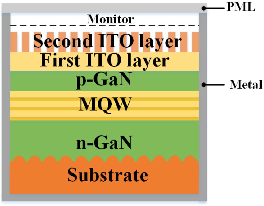
Nanomaterials 2019, 9, 203                                                                                             7 of 9

      Figure 8. (a) L-I characteristic and (b) I–V characteristic of UV LED I, UV LED II, UV LED III, and UV LED IV.

4. Conclusions
     The first unpatterned current spreading layer and the second patterned light extracting layer
were combined into a patterned double-layer ITO to improve current spreading and LEE of UV LEDs.
The interval of the pinhole patterns on the second ITO has a significant impact on the sheet resistance of
patterned double-layer ITO and the way of light propagation at the ITO-air interface. Compared to UV
LED with planar double-layer ITO, LEE of UV LED with a patterned double-layer ITO was improved
due to the scattering out of the waveguided light trapped inside the GaN film. The LOP of UV
LED with a patterned double-layer ITO increased with decreasing interval of the pinhole patterns
due to the higher density of pinhole pattern formed on the second ITO. Owing to non-uniform
current spreading caused by pinhole patterns on the second ITO, the forward voltage of UV LED with
a patterned double-layer ITO was slightly increased.

Author Contributions: S.Z. originally conceived the idea. J.Z. and S.Z. wrote the manuscript. X.D. contributed to
the manuscript preparation. J.M. carried out SEM, TEM, and transmittance measurements. J.H. and H.W. carried
out the simulations. All authors discussed the progress of the research and reviewed the manuscript.
Funding: This work was supported by the National Key R&D Program of China (No. 2017YFB1104900),
the National Natural Science Foundation of China (Grant Nos. 51675386, 51305266), and Hubei Province Science
Fund for Distinguished Young Scholars (No. 2018CFA091). We acknowledge nanofabrication assistance from
the Center for Nanoscience and Nanotechnology at Wuhan University.
Conflicts of Interest: The authors declare no conflict of interest.

References
1.    Zou, X.; Lin, Y.; Xu, B.; Cao, T.; Tang, Y.; Pan, Y.; Gao, Z.; Gao, N. Enhanced inactivation of E. coli by pulsed
      UV-LED irradiation during water disinfection. Sci. Total Environ. 2019, 650, 210–215. [CrossRef] [PubMed]
2.    Rattanakul, S.; Oguma, K. Inactivation kinetics and efficiencies of UV-LEDs against Pseudomonas aeruginosa,
      Legionella pneumophila, and surrogate microorganisms. Water Res. 2018, 130, 31–37. [CrossRef] [PubMed]
3.    Zhou, S.; Xu, H.; Hu, H.; Gui, C.; Liu, S. High quality GaN buffer layer by isoelectronic doping and its
      application to 365 nm InGaN/AlGaN ultraviolet light-emitting diodes. Appl. Surf. Sci. 2019, 471, 231–238.
      [CrossRef]
4.    Oguma, K.; Kanazawa, K.; Kasuga, I.; Takizawa, S. Effects of UV Irradiation by Light Emitting Diodes on
      Heterotrophic Bacteria in Tap Water. Photochem. Photobiol. 2018, 94, 570–576. [CrossRef] [PubMed]
5.    Hu, H.; Zhou, S.; Liu, X.; Gao, Y.; Gui, C.; Liu, S. Effects of GaN/AlGaN/Sputtered AlN nucleation layers on
      performance of GaN-based ultraviolet light-emitting diodes. Sci. Rep. 2017, 7, 44627. [CrossRef] [PubMed]
6.    Guo, H.; Huang, X.; Zeng, Y. Synthesis and photoluminescence properties of novel highly thermal-stable
      red-emitting Na3 Sc2 (PO4 )3 :Eu3+ phosphors for UV-excited white-light-emitting diodes. J. Alloys Compd.
      2018, 741, 300–306. [CrossRef]
Nanomaterials 2019, 9, 203 8 of 9
7. Fernandes, R.A.; Sampaio, M.J.; Da Silva, E.S.; Serp, P.; Faria, J.L.; Silva, C. Synthesis of selected aromatic
aldehydes under UV-LED irradiation over a hybrid photocatalyst of carbon nanofibers and zinc oxide.
Catal. Today 2018. [CrossRef]
8. Zhou, S.; Hu, H.; Liu, X.; Liu, M.; Ding, X.; Gui, C.; Liu, S.; Guo, L.J. Comparative study of GaN-based
ultraviolet LEDs grown on different-sized patterned sapphire substrates with sputtered AlN nucleation
layer. Jpn. J. Appl. Phys. 2017, 56, 111001. [CrossRef]
9. Qian, C.; Li, Y.; Fan, J.; Fan, X.; Fu, J.; Zhao, L.; Zhang, G. Studies of the light output properties for a GaN based
blue LED using an electro-optical simulation method. Microelectron. Reliab. 2017, 74, 173–178. [CrossRef]
10. Hao, G.D.; Taniguchi, M.; Tamari, N.; Inoue, S. Enhanced wall-plug efficiency in AlGaN-based
deep-ultraviolet light-emitting diodes with uniform current spreading p-electrode structures. J. Phys.
D Appl. 2016, 49, 235101. [CrossRef]
11. Kudryk, Y.Y.; Zinovchuk, A.V. Efficiency droop in InGaN/GaN multiple quantum well light-emitting diodes
with nonuniform current spreading. Semicond. Sci. Technol. 2011, 26, 095007. [CrossRef]
12. Huang, S.; Fan, B.; Chen, Z.; Zheng, Z.; Luo, H.; Wu, Z.; Wang, G.; Jiang, H. Lateral current spreading effect
on the efficiency droop in GaN based light-emitting diodes. J. Disp. Technol. 2013, 9, 266–271. [CrossRef]
13. Djavid, M.; Choudhary, D.D.; Philip, M.R.; Bui, T.H.Q.; Akinnuoye, O.; Pham, T.T.; Nguyen, H.P.T. Effects of
optical absorption in deep ultraviolet nanowire light-emitting diodes. Photonics Nanostruct. 2018, 28, 106–110.
[CrossRef]
14. Mock, J.; Bobinger, M.; Bogner, C.; Lugli, P.; Becherer, M. Aqueous Synthesis, Degradation, and Encapsulation
of Copper Nanowires for Transparent Electrodes. Nanomaterials 2018, 8, 767. [CrossRef]
15. Park, J.S.; Kim, J.H.; Na, J.Y.; Kim, D.H.; Kang, D.; Kim, S.K.; Seong, T.Y. Ag nanowire-based electrodes
for improving the output power of ultraviolet AlGaN-based light-emitting diodes. J. Alloys Compd. 2017,
703, 198–203. [CrossRef]
16. Gui, C.; Ding, X.; Zhou, S.; Gao, Y.; Liu, X.; Liu, S. Nanoscale Ni/Au wire grids as transparent conductive
electrodes in ultraviolet light-emitting diodes by laser direct writing. Opt. Laser Technol. 2018, 104, 112–117.
[CrossRef]
17. Alonso, E.T.; Rodrigues, D.P.; Khetani, M.; Shin, D.W.; Sanctis, A.D.; Joulie, H.; Schrijver, I.; Baldycheva, A.;
Alves, H.; Neves, A.I.S.; et al. Graphene electronic fibres with touch-sensing and light-emitting functionalities
for smart textiles. NPJ Flexible Electron. 2018, 2, 25. [CrossRef]
18. Bointon, T.H.; Russo, S.; Craciun, M.F. Is graphene a good transparent electrode for photovoltaics and display
a pplications? IET Circ. Devices Syst. 2015, 9, 403–412. [CrossRef]
19. Alonso, E.T.; Karkera, G.; Jones, G.F.; Craciun, M.F.; Russo, S. Homogeneously bright, flexible, and foldable
lighting devices with functionalized graphene electrodes. ACS Appl. Mater. Interfaces 2016, 8, 16541–16545.
[CrossRef]
20. Wu, Z.; Chen, Z.; Du, X.; Logan, J.M.; Sippel, J.; Nikolou, M.; Kamaras, K.; Reynolds, J.R.; Tanner, D.B.;
Hebard, A.F.; et al. Transparent, Conductive Carbon Nanotube Films. Science 2004, 305, 1273–1276. [CrossRef]
21. Hu, L.; Hecht, D.S.; Grüner, G. Percolation in Transparent and Conducting Carbon Nanotube Networks.
Nano Lett. 2004, 4, 2513–2517. [CrossRef]
22. Park, J.S.; Kim, J.H.; Kim, J.Y.; Kim, D.H.; Kang, D.; Sung, J.S.; Seong, T.Y. Hybrid indium tin oxide/Ag
nanowire electrodes for improving the light output power of near ultraviolet AlGaN-based light-emitting
diode. Curr. Appl. Phys. 2016, 16, 545–548. [CrossRef]
23. Lai, W.C.; Lin, C.N.; Lai, Y.C.; Yu, P.; Chi, G.C.; Chang, S.J. GaN-based light-emitting diodes with
graphene/indium tin oxide transparent layer. Opt. Express 2014, 22, A396–A401. [CrossRef] [PubMed]
24. Kim, Y.H.; Lee, J.; Hofmann, S.; Gather, M.C.; Müller-Meskamp, L.; Leo, K. Achieving High Efficiency
and Improved Stability in ITO-Free Transparent Organic Light-Emitting Diodes with Conductive Polymer
Electrodes. Adv. Funct. Mater. 2013, 23, 3763–3769. [CrossRef]
25. Kim, H.; Lee, S.N. Theoretical considerations on current spreading in GaN-based light emitting diodes
fabricated with top-emission geometry. J. Electrochem. Soc. 2010, 157, H562–H564. [CrossRef]
26. Jo, Y.J.; Hong, C.H.; Kwak, J.S. Improved electrical and optical properties of ITO thin films by using electron
beam irradiation and their application to UV-LED as highly transparent p-type electrodes. Curr. Appl. Phys.
2011, 11, S143–S146. [CrossRef]Nanomaterials 2019, 9, 203 9 of 9
27. Liu, Y.J.; Huang, C.C.; Chen, T.Y.; Hsu, C.S.; Liou, J.K.; Tsai, T.Y.; Liu, W.C. Implementation of
an indium-tin-oxide (ITO) direct-Ohmic contact structure on a GaN-based light emitting diode. Opt. Express
2011, 19, 14662–14670. [CrossRef]
28. Waki, I.; Fujioka, H.; Oshima, M.; Miki, H.; Fukizawa, A. Low-temperature activation of Mg-doped GaN
using Ni films. Appl. Phys. Lett. 2001, 78, 2899. [CrossRef]
29. Nakamura, S.; Mukai, T.; Senoh, M.; Iwasa, N. Thermal annealing effects on p-type Mg-doped GaN films.
Jpn. J. Appl. Phys. 1992, 31, L139. [CrossRef]
30. Zhou, S.; Yuan, S.; Liu, Y.; Guo, L.J.; Liu, S.; Ding, H. Highly efficient and reliable high power LEDs with
patterned sapphire substrate and strip-shaped distributed current blocking layer. Appl. Surf. Sci. 2015,
355, 1013–1019. [CrossRef]
31. Jung, S.H.; Song, K.M.; Choi, Y.S.; Park, H.H.; Shin, H.B.; Kang, H.K.; Lee, J. Light output enhancement of
InGaN/GaN light-emitting diodes with contrasting indium tin-oxide nanopatterned structures. J. Nanomater.
2013, 2013, 7. [CrossRef]
32. Tsai, C.F.; Su, Y.K.; Lin, C.L. Improvement in External Quantum Efficiency of InGaN-Based LEDs by
Micro-Textured Surface with Different Geometric Patterns. J. Electrochem. Soc. 2011, 159, H151–H156.
[CrossRef]
33. Zhong, Y.; Shin, Y.C.; Kim, C.M.; Lee, B.G.; Kim, E.H.; Park, Y.J.; Sobahan, K.M.A.; Hwangbo, C.K.; Lee, Y.P.;
Kim, T.G. Optical and electrical properties of indium tin oxide thin films with tilted and spiral microstructures
prepared by oblique angle deposition. J. Mater. Res. 2008, 23, 2500–2505. [CrossRef]
34. Chang, S.J.; Shen, C.F.; Chen, W.S.; Kuo, C.T.; Ko, T.K.; Shei, S.C.; Sheu, J.K. Nitride-based light emitting
diodes with indium tin oxide electrode patterned by imprint lithography. Appl. Phys. Lett. 2007, 91, 013504.
[CrossRef]
35. Horng, R.H.; Yang, C.C.; Wu, J.Y.; Huang, S.H.; Lee, C.E.; Wuu, D.S. GaN-based light-emitting diodes with
indium tin oxide texturing window layers using natural lithography. Appl. Phys. Lett. 2005, 86, 221101.
[CrossRef]
36. Leem, D.S.; Cho, J.; Sone, C.; Park, Y.; Seong, T.Y. Light-output enhancement of GaN-based light-emitting
diodes by using hole-patterned transparent indium tin oxide electrodes. J. Appl. Phys. 2005, 98, 076107.
[CrossRef]
37. Kang, J.H.; Ryu, J.H.; Kim, H.K.; Kim, H.Y.; Han, N.; Park, Y.J.; Uthirakumar, P.; Hong, C.H. Comparison
of various surface textured layer in InGaN LEDs for high light extraction efficiency. Opt. Express 2011,
19, 3637–3646. [CrossRef]
38. Zhou, S.; Cao, B.; Liu, S.; Ding, H. Improved light extraction efficiency of GaN-based LEDs with patterned
sapphire substrate and patterned ITO. Opt. Laser Technol. 2012, 44, 2302–2305. [CrossRef]
39. Huang, H.; Hu, J.; Wang, H. GaN-based light-emitting diodes with hybrid micro/nano-textured
indium-tin-oxide layer. J. Semicond. 2014, 35, 084006. [CrossRef]
40. Oh, S.; Su, P.C.; Yoon, Y.J.; Cho, S.; Oh, J.H.; Seong, T.Y.; Kim, K.K. Nano-patterned dual-layer ITO electrode
of high brightness blue light emitting diodes using maskless wet etching. Opt. Express 2013, 21, A970–A976.
[CrossRef]
41. Leem, D.S.; Lee, T.; Seong, T.Y. Enhancement of the light output of GaN-based light-emitting diodes with
surface-patterned ITO electrodes by maskless wet-etching. Solid-State Electron. 2007, 51, 793–796. [CrossRef]
42. Markov, L.K.; Smirnova, I.P.; Pavluchenko, A.S.; Kukushkin, M.V.; Zakheim, D.A.; Pavlov, S.I. Use of
double-layer ITO films in reflective contacts for blue and near-UV LEDs. Semiconductors 2014, 48, 1674–1679.
[CrossRef]
© 2019 by the authors. Licensee MDPI, Basel, Switzerland. This article is an open access
article distributed under the terms and conditions of the Creative Commons Attribution
(CC BY) license (http://creativecommons.org/licenses/by/4.0/).You can also read