Simulation of a Charged Al2O3 Film As An Assisting Passivation Layer For a-Si Passivated Contact p- Type Silicon Solar Cells - Research Square
←
→
Page content transcription
If your browser does not render page correctly, please read the page content below
Simulation of a Charged Al2O3 Film As An Assisting
Passivation Layer For a-Si Passivated Contact p-
Type Silicon Solar Cells
Tian Pu ( sherlock.pu@outlook.com )
Nanjing University of Aeronautics and Astronautics https://orcid.org/0000-0002-9428-2656
Honglie Shen
Nanjing University of Aeronautics and Astronautics https://orcid.org/0000-0002-2759-9880
Quntao Tang
Nanjing University of Aeronautics and Astronautics
Research Article
Keywords: Simulation, charged Al2O3 layer, a-Si passivated contact p-type silicon solar cell, HIT solar cell
DOI: https://doi.org/10.21203/rs.3.rs-215611/v1
License: This work is licensed under a Creative Commons Attribution 4.0 International License.
Read Full License
Page 1/12Abstract
In this paper, a charged Al2O3 tunneling lm as an assisting for amorphous Si (a-Si) passivated contact
layer is proposed and theoretically simulated for its potential application in improving a-Si passivated
contact p-type (a-PC-p) solar cell. The concept is based on an Ag/n+ c-Si/p c-Si/Al2O3/p+ a-Si/Al structure.
The key feature is the introduction of a charged Al2O3 layer, which facilitates the tunneling of holes
through an Al2O3 insulator layer accompanied by the reduction of interface defect density (D it). The
negative charge in the Al2O3 layer makes the energy band of p-type c-Si bend upward, realizing the
accumulation of holes and repelling of electrons at the c-Si/a-Si interface simultaneously. The in uence
of interface negative charges (Qit) between a-Si and c-Si, Al2O3 thickness, Al2O3 bandgap, interface defect
density (D it) at the a-Si/c-Si interface are systematically investigated on the output parameters of a-PC-p
cells. Inserting a charged Al2O3 lm between the c-Si/a-Si interface, a +4.2 % relative e ciency gain is
predicted theoretically compared with the a-PC-p cells without the Al2O3 layer. Subsequently, the device
performance under various temperatures is simulated, and the insertion of a charged Al2O3 layer
obviously decreases the Pmax temperature coe cient from -0.336 % /℃ to -0.247 % /℃, which is
analogous to that of Heterojunction with Intrinsic Thin layer (HIT) solar cell. The above results
demonstrate a better temperature response for a-PC-p cells with a charged Al2O3 layer, paving a road for
its potential application in high-e ciency and high thermal stability a-PC-p solar cells.
Highlights
A charged Al2O3 assisting passivation layer is proposed for a-Si PC-p
The Al2O3 layer makes the selective carrier tunneling at the c-Si/a-Si interface.
A +4.2 % relative e ciency gain is predicted theoretically by the Al2O3
The insertion of the Al2O3 layer reduces the Pmax temperature coe cient greatly.
1. Introduction
In the last several years, the a-Si/c-Si passivated contact (a-PC) solar cell has attracted a large amount of
attention due to its prominent high Voc and higher e ciency. A famous example of the a-PC solar cell is
the heterojunction technology (HJT) solar cell which achieves very high conversion e ciency by using
hydrogenated amorphous silicon (a-Si:H) layer to effectively passivate the amorphous and crystalline
silicon (c-Si) interface as well as at the metal contact area[1]. Compared with traditional diffusion
processed homo-junction solar cells, the most attractive advantages of the a-PC solar cell are its lower
deposition temperature (< 200 ℃) and better cell temperature coe cient (-0.25 %)[2]. As is known to all,
the device quality is mainly determined by factors including a-Si emitter quality and interface quality
between a-Si and c-Si. Defect states at the a-Si/c-Si interface could induce strong interface recombination
in an a-PC solar cell if the interface defect density is larger than 1×1013 cm-2·eV-1. The mid-gap with a low
Page 2/12interface state can be achieved by the insertion of intrinsic hydrogenated amorphous silicon. However,
the narrow process window for depositing intrinsic hydrogenated amorphous silicon makes it very easy
to grow epitaxially on the c-Si substrate[3]. The detrimental effect of an epitaxially grown interface
normally causes a Voc of a-PC solar cell lower than 600 mV. The defects in the epitaxial lm are
determined by the energy position within the bandgap and the capture cross-section of the electron and
hole. Usually, an abruptness of the a-Si/c-Si interface without any initial epitaxial growth is more
preferred. Therefore, a tunnel oxide insulator layer (usually SiO2), is adopted to prohibit the epitaxial
phenomenon and reduce recombination at the interface[4-5]. Generally speaking, the used SiO2 should be
as thin as possible to ensure the tunneling process (< 20 Å), while the interface passivation effect will be
better if a thicker oxide layer is adopted. As a result, a trade-off between the tunneling process and
interface passivation should be considered.
Generally speaking, a solar cell is based on a semiconductor material that absorbs light and then
generates excess electrons and holes. The different types of contacts in a solar cell not only conduce to
collect the different charge carriers but also serve as a semipermeable membrane so that one contact
supports electrons getting across and blocks holes, while the other contact is exactly the opposite. Except
being carrier-selective, the contacts are better to passivate the surface defects to ensure that the minority
carriers are collected before their recombination. Such contacts can therefore be de ned as contact
passivation[6]. Recently, there has been an increasing interest in the application of tunneling layers for
passivation contact in single-junction silicon-based solar cells. The used a-Si stack layer in HIT solar cells
[7] and SiO2/polycrystalline silicon stack layer[8] in high-e ciency n-type silicon solar cells are all, in fact,
contact passivation structures. Therefore, the contact passivation structure is usually made of an
ultrathin insulator layer and a highly doped semiconductor layer. The used insulator materials can be
positively charged layers, i.e., a-SiNx: H[9] and thermal SiO2[10], which can lead to an effective surface
passivation result on lightly doped n- or p-type substrate, as well as some negatively charged layer such
as Al2O3[11]. Negative charges in Al2O3 are particularly suited to passivate the backside of the p-type solar
cell. It is expected that the negative charges in Al2O3 can repel electrons and accumulate holes at the
interface between a-Si and c-Si, which increases the probability of tunneling through the Al2O3 layer.
Aluminum oxide (Al2O3) has potentially been used as an optional passivation material to standard a-
SiNx: H. The application of Al2O3 here could be summarized by two important trends. First, the
photovoltaic (PV) industry has recently transferred the Al-back surface eld (Al-BSF) cell to a dielectrically
rear passivated cell[12-14]. This rear side passivated structure leads to a lower surface recombination loss,
better light re ection inside the cell, and less suffered wafer bow for thinner wafers[15-17]. A passivated
rear side is believed necessary for higher conversion e ciency and the possibility of thinner Si wafers
application. Though the ultrathin SiO2 layer has been widely used in a-PC solar cells, the use of an
ultrathin Al2O3 layer as a tunnel oxide layer in contact passivation structure is rarely reported. Therefore, it
is necessary for understanding how the parameters affecting tunneling, for example, the negative
Page 3/12charges (Qit) in the a-Si and c-Si interface, Al2O3 thickness, interface defect density (D it) between a-Si and
c-Si.
In this paper, a p-type c-Si substrate a-Si passivated contact solar cell based on Ag/n+ c-Si/p c-
Si/Al2O3/p+ a-Si/Al structure has been developed to study the variation of Qit between a-Si and c-Si, Al2O3
thickness, Al2O3 bandgap and D it at the a-Si/c-Si interface on a-PC cell performance using AFORS-HET
software. The purpose of this paper is to investigate the in uence of the charged Al2O3 layer on a-PC
cell’s performance, so the reference cell is not optimized.
2. Simulation Models
2.1. Tunneling theory
As direct quantum tunneling, the calculation of electron tunnel current Je, tun is based on the Tsu–Esaki
equation18] in semiconductor-insulator-semiconductor (SIS) structures:
where q is the elementary charge, Emin is the minimum conduction band edge energy to have tunneling
effect, m* is the tunneling effective mass and h is Planck's constant. The barrier transparency T(E) gives
the probability of an electron with the energy E through the barrier to the tunnel.
With known effective masses for silicon, the result outside the integration sign is a constant. As a result,
the tunneling current is dominated by the quasi-Fermi levels, the energy of the charge carriers and the
transmission coe cient. This coe cient is the ratio of the outgoing compare with incoming ux, is found
using the transfer matrix method to solve the Schrödinger equation. The major parameters are the height
of the energy barrier, the mass of the tunneling effect and the thickness of the oxide.
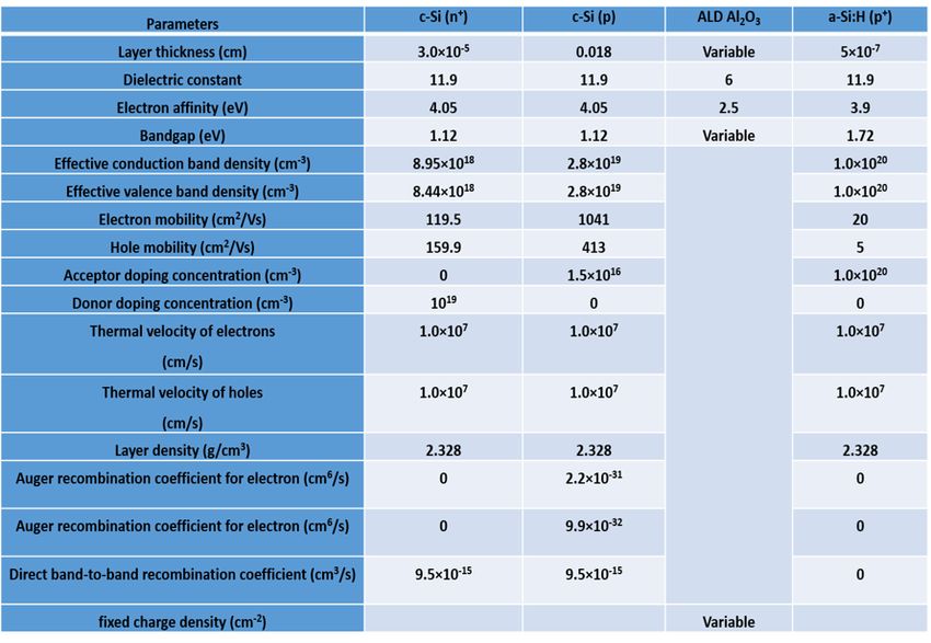
2.2. Simulation parameters
We use the 1D simulation software “Automat FOR Simulation of HETerostructure” (AFORS-HET)
developed at the Helmholtz Zentrum Berlin[19] to perform the numerical simulation in this case. AFORS-
HET could solve one-dimensional semiconductor equations related to Shockley–Reed–Hall statistics. It
utilizes an optical model based on the Lambert-Beer law for calculating the optical parameters. In this
article’s simulation, we assumed that the metal contacts are a at band and the solar radiation AM 1.5
with a power density of 100 mW/cm2 is introduced as a light source. The gap statistics of various types
of a-Si:H layers and c-Si wafer are de ned as a default value in the AFORS-HET con guration. Simulated
cell structure with the position of the different layers is presented in Fig.1. The layer’s given parameters
are presented in Table 1.
Table 1 Input parameters used in the present simulation
Page 4/12At the rear side hetero-interface, defects are considered using a 1 nm thick highly defective c-Si interfacial
layer which contains two Gaussian distributed density of states (DOS)[20]. The Gaussian distributions of
donor-like and the acceptor-like have their maximum at 0.56 eV and 0.76 eV above the valence band (Ev).
The standard deviation of both distributions is 0.2 eV and the electron and holes capture cross-sections
(σe, σh) are 1×10-14 cm-2. Their heights are adjusted to the equivalent interface defect densities (cm-2),
which is yield targeted.
Regarding the carrier transport mechanism, we assume drift-diffusion for c-Si/c-Si (homo-interfaces) and
consider tunneling thermionic emission for c-Si/a-Si:H (hetero-interfaces). Here we should also consider a
high doping level of the added a-Si layer will induce the bandgap narrowing.
The electrical current through the two semiconductors’ interface is virtually the current that would ow
through a ctitious insulating layer by tunneling in this simulation using AFROS-HET software. The
conduction mechanism in this simulated structure could be explained as a hole tunneling from the
valence band of the base p-type c-Si through the Al2O3 layer, then into the p+ a-Si:H layer. The effective
mass of bulk Al2O3 is 3-10 m0, while an effective mass of 0.33 m0 has been found for tunnel thin
layers[21]. So the input effective mass of Al2O3 is set to 0.33 m0. Bulk Al2O3 in the crystalline phase has a
Page 5/12bandgap of about 8.8 eV. For the atomic layer deposition deposited amorphous Al2O3 layer has a
bandgap of about 6.4 eV[22]. This has been used unless stated otherwise. The dielectric constant and
electron a nity values of the ultrathin Al2O3 layer are set according to the results reported in the literature
[22].
3. Results And Discussion
Along with the introduction of Aluminum oxide (Al2O3) comes the introduction of atomic layer deposition
(ALD) in the photovoltaic industry. ALD is different from conventional plasma-enhanced chemical vapor
deposition tools due to the strict separation of the process gases in two half-cycles during deposition,
resulting in a self-limited layer-by-layer growth. The strength of ALD is precisely thickness control and
very good deposition uniformity over large area surfaces. Generally speaking, the excellent passivation
performance of ALD Al2O3 originates from the combination of low D it (chemical passivation) and high Qit
( eld-effect passivation)[23]. The as-deposited thermal ALD Al2O3 usually possesses a relatively low D it
accompanied with a low value of Qit while the as-deposited plasma ALD provides high D it and high Qit.
With extra annealing treatment, both ALD processes show lower D it ≤ 1×1011 cm-2[24-25]. Regarding the
eld-effect passivation, the thermal ALD-based Al2O3 lm exhibits especially low Qit of the order of 1011
cm-2 before annealing comparing to plasma ALD with Qit of the order of 1012 cm-2. Also, the highest Qit
value for plasma ALD can reach 1013 cm-2[26-28] after annealing. Therefore, for the ALD Al2O3 lm, Qit can
be adjusted from 1×10¹⁰~1013 cm-2 by choosing different ALD processes and post-annealing treatment.
To investigate the in uence of Qit at p-type c-Si/ALD Al2O3 interface on simulated a-PC-p cell’s output
parameters, Qit is adjusted from 1×10¹⁰~1013 cm-2 with D it xed at 1011 cm-2. Fig.2 presents the
simulated a-PC-p cell’s output parameters versus Qit. It is seen that the cell’s performance is enhanced
with increasing Qit from 1010 cm-2 to 1013 cm-2. In the low Qit (< 1012 cm-2 ) region, the amount of Qit is
not enough to assist hole tunneling through the Al2O3 layer, as a result of which low Jsc and low FF
appear. When Qit increases from 1012 cm-2 to 1013 cm-2, Jsc and e ciency increase while FF rarely
changes. Therefore, it is suspected that enough amount of Qit can ensure the tunneling process even
though a dielectric layer is used. This is consistent with the result reported in the literature[28].
As the ALD Al2O3 layer thickness can in uence the tunneling of carriers, various levels of Al2O3 layer
thickness are adopted to study its effect on simulated a-PC-p cell’s output parameters (shown in Fig.3).
To understand how Qit affects the Al2O3 layer of different thicknesses, Al2O3 layers of various
thicknesses with and without Qit are introduced (shown in Fig.3). For the Al2O3 layer without Qit, the cell’s
FF decreases rapidly from 80.89 % to 49.33 % with Al2O3 thickness increasing from 0.2 nm to 0.4 nm.
And FF, Jsc and e ciency are reduced to 40.66 %, 0.32 mA/cm-2 and 0.087 %, respectively, when Al2O3
thickness further increases to 1 nm. However, for the Al2O3 layer with -1013 cm-2 Qit, both FF and
e ciency of the cell rarely change even when increasing Al2O3 thickness to 1 nm. This demonstrates the
Page 6/12vital role Qit plays in carrier tunneling. When Al2O3 thickness exceeds 1 nm, the cell with -1013 cm-2 Qit
loses its Jsc and e ciency rapidly, while its FF still rarely changes. Theoretically, the thicker the Al2O3
layer is, the lower the tunneling probability (T(E)) for carriers will be. Therefore, a thinner Al2O3 is desired
for a high tunneling current. Besides, the added Qit facilitates the alignment of the energy bands for both
c-Si and a-Si, and causes the accumulation of holes at their interface, which results in a higher built-in
potential. Therefore, the enhanced built-in potential facilitates the tunneling of holes through the barrier.
According to the simulated results shown in Fig.2 and Fig.3, Qit at the c-Si/a-Si interface have a
signi cant in uence on carrier transport through the Al2O3 dielectric layer. Qit can maintain the successful
tunneling of carriers without degrading the cell’s performance. To gure out how Qit in uences the
transport of carriers through the Al2O3 dielectric layer, band diagram and carrier distribution with the
position of two different cells are calculated and compared. The Al2O3 dielectric layer thickness for both
cells is xed at 1 nm. The only difference between the two cells is that one cell has a Qit of -1013 cm-2,
while the other has a Qit of 0 cm-2. As shown in Fig.4 (a) and (b), the band diagram of the cell with a Qit of
-1013 cm-2 bends upward compared to the other cell, indicating that the high Qit leads to an accumulation
of holes at the interface. Fig.4 (c) shows the density of electron and hole at the c-Si/a-Si interface, a large
number of holes with an order of 1013 cm-3 accumulated on the c-Si side accompanied by a smaller
amount of electrons for the cell with a Qit of 1013 cm-2. Cell with a Qit of 0 only has a much smaller
amount of electrons and holes on the c-Si side. This reveals the fact that Qit can in uence the carrier
distribution at the c-Si/a-Si interface and thus the selective transport of carriers through the dielectric
layer. Based on the above three gures, a schematic band diagram illustrating how the charged Al2O3
layer affecting the transport behavior of electrons and holes is shown in Fig.4 (d). As can be seen, the
charged Al2O3 layer behaves like a lter which can allow the transport of holes through it with repelling
electrons backward.
The oxide bandgap (Eg) can also affect the magnitude of the effect caused by the charges. A difference
in the bandgap of Al2O3 has been gured for different deposition processes, there is a variation from 6.2
eV to 7.0 eV was found in the literature[29,30]. In Fig.5, the simulated a-PC-p cell’s four output parameters
as a function of the Al2O3 bandgap are shown for Qif value of -1013cm-2. The cell’s e ciency is mainly
in uenced by the change of Jsc and FF. When Eg is less than 6.7eV, the decrease of e ciency along with
increasing Eg is due to the decrease of FF. However, when Eg is bigger than 6.7eV, the loss of e ciency is
mostly determined by the decrease of Jsc. It is expected that the barrier height at the c-Si/a-Si interface
can be modeled by choosing the Al2O3 layer of different Eg. Therefore, selecting a bigger Eg Al2O3 layer
means higher barrier height at the c-Si/a-Si interface, which results in a relatively low tunneling
probability, and thus a low FF and a low Jsc.
We know that the interface defect density (D it) has a great in uence on c-Si/a-Si interface recombination.
The distribution of D it at the c-Si/a-Si interface is a state’s superposition near band edges and states.
Page 7/12These states include surface pretreatment-induced strain bonds, bonds between adsorbates, dangling
bonds, and atoms of different oxide layers leading to several groups of interface states. The minimum
value for these interface state distributions can be considered as a measurement of the electronic quality
of the wafer and interface. Fig.6 shows the dependence of simulated a-PC-p cells’ output parameters on
D it. As can be seen, the output parameters of a-PC-p cells, whether with or without the charged Al2O3 layer,
tend to decrease with increasing D it. When D it is less than 1×1013 cm-2, the a-PC-p cell with charged Al2O3
layer possesses a higher e ciency than that without charged Al2O3 layer. However, the tendency operates
in the opposite way when D it is over 1×1013 cm-2, indicating that the D it can have different effects on cell
e ciency for different cells in different D it regions. As is known to all, D it at the a-Si/c-Si interface is more
than 1×1013 cm-2 and the Al2O3 layer can supply a certain extent of interface passivation. Therefore, the
a-PC-p cell’s e ciency can be improved by inserting charged Al2O3 at the a-Si/c-Si interface. Compared
with directly deposited a-Si on the c-Si surface, the presence of the charged Al2O3 can reduce D it and thus
higher e ciency can be obtained.
Fig.7 (a) shows a comparison of the I-V characteristics of a simulated cell with only a-Si and with a-Si
plus Al2O3 at c-Si/p+ a-Si interface, assuming a xed interface charge density (Qit) of -1×1013 cm-2. The
simulation shows that there is a large e ciency gain (4.2 % relative) when changing from a pure a-Si to a-
Si plus Al2O3 (Qit = -1×1013 cm-2) at the c-Si/Al interface. Notably, there is a change of the I-V parameters
of the solar cells, i.e., not only an improvement in Voc and Jsc, but also a reduction in FF (see in the inset
table in Fig.7 (a)). Voc is improved by reducing the interface recombination within the hole collecting
region. Compared with pure p+ a-Si, the addition of a charged Al2O3 layer can reduce a partial portion of
D it by saturating some dangling bonds at the c-Si/p+ a-Si interface (D it is reduced from 1013 cm-2 to 1011
cm-2). A relative Jsc boost of 5.4 % is observed for the cell with the Al2O3 layer. Comparing the spectral
response of simulated cell with only a-Si and with a-Si plus Al2O3 at c-Si/p+ a-Si interface, it is seen that
the external quantum e ciency (EQE) increase from 800 nm to 1100 nm (seen in Fig.7 (b)), which is the
absorption region of the backside. Below 800 nm, the spectral response is almost the same. In the
wavelength region from 800 nm to 1000 nm, EQE increases. As the front side is the same for both cells,
the change of EQE between 800 ~ 1000 nm must be due to the insertion of the Al2O3 layer at the c-Si/p+
a-Si interface. It is expected as light in this region is mostly absorbed in the 180 µm thick p-type base, Qit
increases built-in potential at c-Si/p+ a-Si interface which ultimately boosts the number of holes collected
at the cell’s backside. This can mostly stem from the enhanced interface passivation effect due to the
Al2O3 layer. Though a relative FF decrease of 3.0 % occurs, which may be due to the insertion of 1 nm
Al2O3 layer, a high FF still maintains in comparison to the Al2O3 layer without Qit (as discussed in Fig.3).
As discussed before, the cell with the Al2O3 layer and Qit has a higher built-in potential, and thus
enhances hole collection which leads to a relatively high FF.
To evaluate the device performance under various temperatures, the temperature response of the a-PC-p
cells with and without charged Al2O3 layer is shown in Fig.8, where the e ciency can also represent the
Page 8/12maximum output power. The temperature dependences of Voc, Jsc, FF and e ciency are illustrated by
Fig.8 (a)-(d), respectively. As the temperature increases from 26.85 ℃ to 76.85 ℃, Jsc is enhanced;
whereas both Voc and e ciency drop; FF uctuates as the temperature changes. Based on the simulated
results, a linear tting is adopted to calculate the temperature coe cients of Voc, Jsc, FF and e ciency,
respectively. The obtained temperature coe cients for both cells are listed in Table 2. As can be seen, the
insertion of a charged Al2O3 layer drops the Pmax temperature coe cient from -0.336 % / ℃ to -0.247 % /
℃, indicating that the output power degrades less with increasing working temperature. Simultaneously,
the Voc temperature coe cient also drops for the better interface passivation of charged Al2O3 layer. The
above results demonstrated a better temperature response for the a-PC-p cell with a charged Al2O3 layer,
paving a road for its potential application in high-e ciency and high thermal stability a-PC-p solar cells.
Table 2 Simulated temperature coe cients of Voc, Jsc, FF and e ciency.
4. Conclusions
In this study, we theoretically investigate the charged Al2O3 lm as an assisting passivation layer in
improving the performance of the p-type silicon-based a-Si passivated contact solar cell (Ag/n+ c-Si/p c-
Si/Al2O3/p+ a-Si/Al structure). The purpose of the charged Al2O3 tunnel lm is to realize the accumulation
of holes and simultaneously to enhance the c-Si/a-Si interface passivation, which facilitates the
tunneling of holes through the Al2O3 insulator layer and the reduction of interface defect density (D it)
respectively. Through the systematic optimization of interface negative charges (Qit) between a-Si and c-
Si, Al2O3 thickness, Al2O3 bandgap, and interface defect density (D it) at a-Si/c-Si interface, a +4.2 %
relative e ciency gain is predicted theoretically compared with the a-PC-p cell without Al2O3 layer. Based
on the temperature-dependent investigation of output parameters of both a-PC-p cells, the decrease of the
Pmax temperature coe cient from -0.336 % /℃ to -0.247 % /℃ is observed by the insertion of a charged
Page 9/12Al2O3 layer. The above results demonstrate the better performance of a-PC-p cell with a charged Al2O3
layer, indicating its potential application in high-e ciency and high thermal stability a-PC-p solar cells.
Declarations
Funding statement
This work has been nancially supported by the National Nature Science Foundation of China
(61774084), the open project of Key Laboratory of Materials Preparation and Protection for Harsh
Environment, Ministry of Industry and Information Technology (XCA20013-3) and the Special Scienti c
Innovation Fund of Sihong County (H201901).
Con ict of Interest
We declare that we have no nancial and personal relationships with other people or organizations that
can inappropriately in uence our work, there is no professional or other personal interest of any nature or
kind in any product, service and/or company that could be construed as in uencing the position
presented in, or the review of, the manuscript entitled.
Author contributions
Conceptualization, Tian Pu.; software, Quntao Tang.; formal analysis, Tian Pu.; investigation, Tian Pu.,
Quntao Tang; resources, Honglie Shen.; data curation, Quntao Tang; writing—original draft preparation,
Tian Pu.; writing—review and editing, Quntao Tang., Honglie Shen.; visualization, Tian Pu.; project
administration, Honglie Shen.; funding acquisition, Honglie Shen. All authors have read and agreed to the
published version of the manuscript.
Availability of data and material
The datasets generated during and/or analysed during the current study are available from the
corresponding author on reasonable request.
Compliance with ethical standards
Con ict of Interest: The authors declare that they have no con ict of interest.
Research involving human participants and/ or animals: Not applicable
Informed consent: Informed consent was obtained from all individual participants included in the study.
Consent to participate
Not applicable
Consent for Publication
Page 10/12Not applicable
References
1. Park H, Lee YJ, Park J et al (2018) Front and Back TCO Research Review of a-Si/c-Si Heterojunction
with Intrinsic Thin Layer (HIT) Solar Cell[J]. Trans Electr Electron Mater 19:165–172
2. Haschke J, Dupré O, Boccard M et al (2018) Silicon heterojunction solar cells: Recent technological
development and practical aspects - from lab to industry[J]. Solar Energy Materials Solar Cells
187(1):140–153
3. Balaji P, Dauksher WJ, Bowden SG et al (2020) Improving surface passivation on very thin substrates
for high e ciency silicon heterojunction solar cells[J]. Sol Energy Mater Sol Cells 216:110715
4. Liu W, Meng F, Zhang X et al (2015) Evolution of native oxide layer at a-Si:H/c-Si interface and its
in uence on silicon heterojunction solar cell.[J]. Angew Chem 51(3):748–751
5. Choi S, Min KH, Jeong MS (2017) Structural evolution of tunneling oxide passivating contact upon
thermal annealing[J]. Scienti c reports 7(1):12853
6. Limodio G, Yang G, Ge H et al (2019) Front and rear contact Si solar cells combining high and low
thermal budget Si passivating contacts[J]. Sol Energy Mater Sol Cells 194(1):28–35
7. Xiao S, Zhou J, Huang S et al. Highly textured conductive and transparent ZnO lms for HIT solar cell
applications[J]. Journal of Physics D Applied Physics, 2015, 48(30)
8. Morisset A, Cabal R, Grange B et al (2019) Highly passivating and blister-free hole selective poly-
silicon based contact for large area crystalline silicon solar cells[J]. Sol Energy Mater Sol Cells
200(15):109912
9. Hintzsche LE, Fang CM, Marsman M et al (2015) Formation of a Positive Fixed Charge at c – Si
(111)/a – Si3N3.5: H Interfaces[J]. Phys Rev Appl 3(6):064005
10. Liu W, Yang X, Kang J et al (2019) Polysilicon Passivating Contacts for Silicon Solar Cells: Interface
Passivation and Carrier Transport Mechanism[J]. ACS Appl Energy Mater 2(7):4609–4617
11. Bansal A, Srivastava P, Singh BR (2015) On the surface passivation of c-silicon by RF sputtered Al2O3
for solar cell application[J]. J Mater Sci: Mater Electron 26(2):639–645
12. Blakers A (2019) Development of the PERC Solar Cell[J]. IEEE J Photovolt 9(3):629–635
13. Hsu CH, Cho YS, Wu WY,, et al (2019) Enhanced Si Passivation and PERC Solar Cell E ciency by
Atomic Layer Deposited Aluminum Oxide with Two-step Post Annealing[J]. Nanoscale Res Lett
14:139
14. Liu PK, Cheng YL, Wang L et al. Crystalline Silicon PERC Solar Cell with Ozonized AlOx Passivation
Layer on the Rear Side[J]. International Journal of Photoenergy, 2020, 2020:6
15. Allen TG, Bullock J, Yang X (2019) Passivating contacts for crystalline silicon solar cells[J]. Nature
Energy 4:914–928
Page 11/1216. Gakis GP, Vahlas C, Vergnes H et al (2019) Investigation of the initial deposition steps and the
interfacial layer of Atomic Layer Deposited (ALD) Al2O3 on Si[J]. Appl Surf Sci 492:245–254
17. Ye F, Yuan N, Ding J et al (2015) The performance of thin industrial passivated emitter and rear
contacts solar cells with homogeneous emitters[J]. J Renew Sustain Energy 7(1):013122
18. Schulman JN (1998) Extension of Tsu-Esaki model for effective mass effects in resonant
tunneling[J]. Applied physics letters 72(22):2829–2831
19. Physics and Technology of Amorphous-Crystalline Heterostructure Silicon Solar Cells, edited by W. G.
J. H. M. van Sark, L. Korte, and F. Roca (Springer Berlin, Heidelberg, 2012), Chap. 4
20. Huang R, Yu M, Yang Q et al (2020) Numerical simulation for optimization of an ultra-thin n-type
WS2/p-type c-Si heterojunction solar cells[J]. Comput Mater Sci 178:109600
21. Vexler MI, Tyaginov SE, Shulekin AF (2005) Determination of the hole effective mass in thin silicon
dioxide lm by means of an analysis of characteristics of a MOS tunnel emitter transistor[J]. J Phys:
Condens Matter 17(50):8057
22. Huang H, Modanese C, Sun S (2018) Effective passivation of p + and n + emitters using
SiO2/Al2O3/SiNx stacks: Surface passivation mechanisms and application to industrial p-PERT
bifacial Si solar cells [J]. Sol Energy Mater Sol Cells 186:356–364
23. Hoex B, Gielis JJH, Van de Sanden MCM et al (2008) On the c-Si surface passivation mechanism by
the negative-charge-dielectric Al2O3[J]. J Appl Phys 104(11):113703
24. Li J, Wang Y, Wan F et al (2020) Passivation via atomic layer deposition Al2O3 for the performance
enhancement of quantum dot photovoltaics[J]. Sol Energy Mater Sol Cells 209(1):110479
25. Lee CY, Deng S, Zhang T et al (2018) Evaluating the impact of thermal annealing on c-Si/Al2O3
interface: Correlating electronic properties to infrared absorption [J]. AIP Adv 8:075204
26. Hezel R, Jaeger K (1989) Low-temperature surface passivation of silicon for solar cells[J]. J
Electrochem Soc 136(2):518–523
27. Banerjee S, Das MK (2021) A review of Al2O3 as surface passivation material with relevant process
technologies on c-Si solar cell[J]. Opt Quant Electron 60:53
28. Li S, Yang N, Yuan X et al (2019) Plasma-induced damage and annealing repairing in ALD-
Al2O3/PECVD-SiNx stack[J]. Mater Sci Semicond Process 100:214–219
29. Roy AM, Lin J, Saraswat KC. The effect of xed charge in tunnel-barrier contacts for Fermi-level
depinning in germanium[J]. Electron Device Letters, IEEE, 2012, 33(6): 761–763
30. Bersch E, Rangan S, Bartynski RA et al (2008) Band offsets of ultrathin high-κ oxide lms with Si[J].
Physical review B 78(8):085114
Page 12/12You can also read