Novel semiconductor detectors for fundamental and applied research - Indico
←
→
Page content transcription
If your browser does not render page correctly, please read the page content below
JOINT INSTITUTE FOR NUCLEAR RESEARCH
                 Dzhelepov Laboratory of Nuclear Problems

                                  Project
Novel semiconductor detectors for fundamental and
                applied research

                     Report and Proposal for prolongation

Project leader: G. Shelkov
Deputy Project Leader: A. Zhemchugov

                               Project members

DLNP: S. Abu Al Azm, M. Demichev, D. Dedovich, V. Elkin, A. Gongadze, M. Gostkin,
      A. Guskov, S. Kotov, D. Kozhevnikov, V. Kruchonok, N. Kuznetsov,
      A. Lapkin, A. Leyva Fabelo, A. Nozdrin, V. Pavlov, I. Potrap, S. Porokhovoy,
      P. Smolyanksiy, V. Tokareva
VBLHEP: A. Averyanov, A. Korotkova, D. Krivenkov, J. Lukstins, A. Maximchuk,
      S. Starikova
FLNR: S. Mitrofanov

                                    Dubna
                                     2017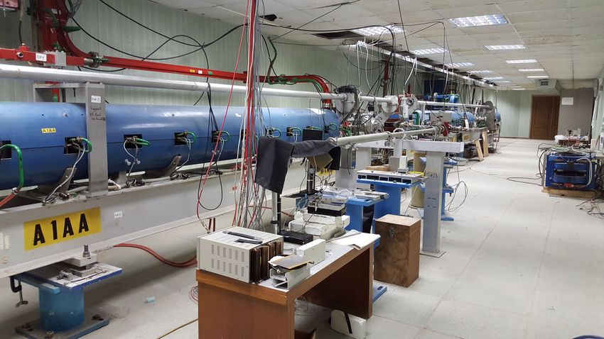
Contents
1 Project goals 3
2 Investigations of semiconductor detectors for nuclear physics and particle physics 7
2.1 Main results in 2015-2017 . . . . . . . . . . . . . . . . . . . . . . . . . . . . . . . 9
2.1.1 Investigation of radiation hardness of detectors based on gallium arsenide 9
2.1.2 Development of FCAL calorimeter for future electron-positron colliders . . 13
2.1.3 X-ray imaging detectors of large area . . . . . . . . . . . . . . . . . . . . . 14
2.1.4 Hybrid pixel detectors based on the Timepix readout chip . . . . . . . . . 17
2.1.5 Pixel detectors as elements of tracking systems . . . . . . . . . . . . . . . 22
2.2 Research program for 2018-2020 . . . . . . . . . . . . . . . . . . . . . . . . . . . . 24
2.2.1 Searches for methods to increase the radiation hardness of gallium arsenide
detectors . . . . . . . . . . . . . . . . . . . . . . . . . . . . . . . . . . . . 24
2.2.2 Identi
cation of particles in hybrid pixel detectors . . . . . . . . . . . . . 24
2.2.3 Neutron registration . . . . . . . . . . . . . . . . . . . . . . . . . . . . . . 25
2.2.4 Studies of hybrid pixel detectors response to the passage of heavy charged
particles . . . . . . . . . . . . . . . . . . . . . . . . . . . . . . . . . . . . . 27
2.2.5 Application of pixel detectors in experiments with hypernuclei and rela-
tivistic ions on the Nuclotron . . . . . . . . . . . . . . . . . . . . . . . . . 28
3 Research infrastructure in the DLNP of JINR 30
3.1 Main results in 2015-2017 . . . . . . . . . . . . . . . . . . . . . . . . . . . . . . . 30
3.1.1 Kalan measuring station . . . . . . . . . . . . . . . . . . . . . . . . . . . 30
3.1.2 Testing bench based on a probe station . . . . . . . . . . . . . . . . . . . 30
3.1.3 Station for measuring charge collection e
ciency . . . . . . . . . . . . . . 31
3.1.4 Installation for ultrasonic microwelding . . . . . . . . . . . . . . . . . . . . 32
3.1.5 Feasibility studies of the site for assembling of hybrid pixel detectors . . . 34
3.2 Scanner for microtomography . . . . . . . . . . . . . . . . . . . . . . . . . . . . . 36
3.3 Development program for 2018-2020 . . . . . . . . . . . . . . . . . . . . . . . . . 38
3.3.1 Site for characterisation of hybrid pixel detectors . . . . . . . . . . . . . . 38
3.3.2 Site for microtomography . . . . . . . . . . . . . . . . . . . . . . . . . . . 39
3.3.3 Development of readout electronics based on the Medipix4 chip . . . . . . 39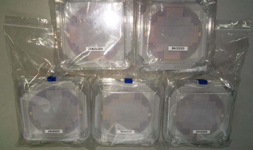
4 Applied research 42
4.1 Main results in 2015-2017 . . . . . . . . . . . . . . . . . . . . . . . . . . . . . . . 42
4.1.1 Investigation of roentgen contrast substances. Studies of possibility of
identifying contrast agents by spectral information. . . . . . . . . . . . . . 42
4.1.2 Investigation of native specimens for analysis of atherosclerotic vascular
damage . . . . . . . . . . . . . . . . . . . . . . . . . . . . . . . . . . . . . 43
4.1.3 Investigation of native specimens for analysis of abdominal aortic aneurysms 44
4.1.4 Analysis of composition of ores and minerals . . . . . . . . . . . . . . . . 44
4.1.5 Investigation of core of oil and gas bearing rocks . . . . . . . . . . . . . . 47
4.2 Research program for 2018-2020 . . . . . . . . . . . . . . . . . . . . . . . . . . . . 47
5 Publications in 2015-2017 49
6 The Project implementation plan 51
6.1 Cost estimates for the Project . . . . . . . . . . . . . . . . . . . . . . . . . . . . . 51
6.2 List of equipment . . . . . . . . . . . . . . . . . . . . . . . . . . . . . . . . . . . . 52
6.3 Scienti
c cooperation . . . . . . . . . . . . . . . . . . . . . . . . . . . . . . . . . . 53
3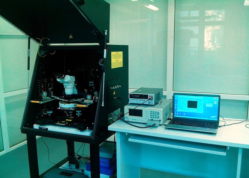
Abstract
Since 2006, the DLNP has been researching and developing semiconductor detectors for
fundamental and applied research on the basis of a new material - chromium-compensated
gallium arsenide (GaAs:Cr), produced at the Laboratory of Functional Electronics of
Tomsk State University. Over the years, including the last three years of the proposed
Project, more than a hundred prototypes of GaAs:Cr sensors have been developed and
manufactured for semiconductor detectors used in a wide range of
elds of science and
technology, from high-energy physics to computed tomography; infrastructure was created
to measure characteristics and study properties of semiconductor materials and detectors
based on them; scienti
c contacts were established with the world centers conducting
similar research, and a number of joint research projects were carried out.
The experience of production and operation of semiconductor detectors based on mod-
i
ed gallium arsenide accumulated in the DLNP allows to proceed both in solving more
complicated problems in the chosen
elds of research and in searching for new applications
for such detectors.
In the course of further development of the Project, it is planned to conduct new
scienti
c and methodological research, in particular, to search for ways to increase the ra-
diation hardness of gallium arsenide based detectors, to identify particles by cluster type
in hybrid pixel detectors, to develop pixel detectors for experiments with hypernuclei and
relativistic ions on the Nuclotron. It is also planned to improve the existing research
infrastructure at the DLNP, including creation of a station for deep level relaxation spec-
troscopy (DLTS) and mastering of this technique, creation of another microtomograph
with a
xed detector and a rotating sample table capable of achieving a spatial resolution
of 5-7 µm due to geometric magni
cation, creation of a full-featured readout electronics
unit for acquisition of data from the Medipix-4 chip. The development of software for
modeling and reconstruction of tomograms will continue, with emphasis on improving the
quality of images, the use of fast algorithms for processing large volumes of tomographic
data and new hardware capabilities.
In the
eld of applied research with the use of methods of spectral microtomography
we will continue to study, in particular, the possibility of predicting the development
of vascular arteriosclerosis based on measurements of the
ne structure of calcium de-
posits in the walls of atherosclerotically aected carotid arteries and aortic aneurysms,
the identi
cation of adipose tissue in animals by combining information on the density
and energy dependence of the linear attenuation coe
cient, the possibility of isolating
roentgen contrast substances in the body for the delivery of drugs to the needed tissue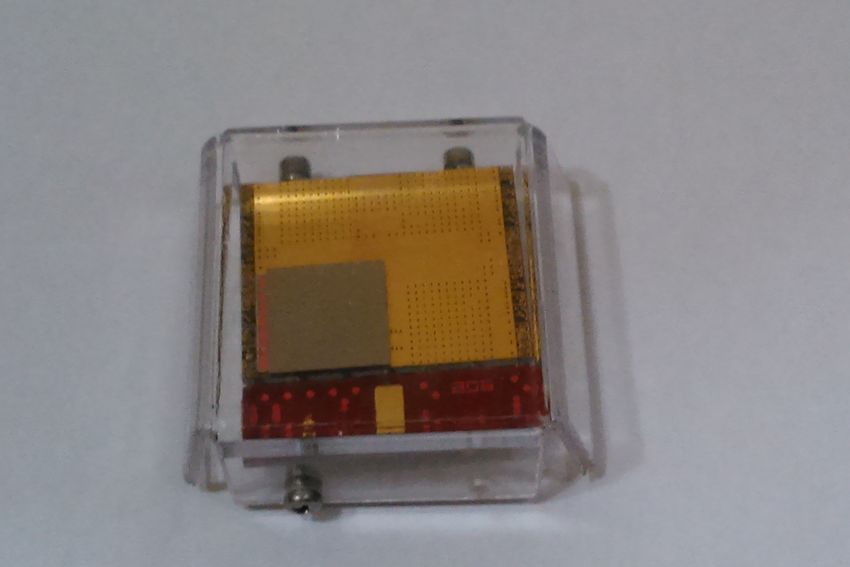
by using radiopaque markers, the identi
cation of mineral phases in ore and mineral raw
materials. The possibility of creating microdosimetric probes based on Timepix detectors
for measuring the equivalent dose of irradiation will also be studied.
The requested amount of funding for the implementation of the Project is 450 thousand
US dollars for three years.
2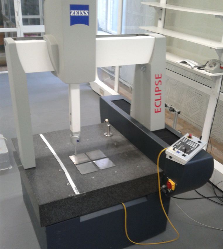
Chapter 1
Project goals
The success of a scienti
c experiment crucially depends on the equipment that it uses.
To a large extent, the progress in understanding of the physical picture of the world that
has occurred over the last century has been provided by technological achievements that
allowed creation of more advanced experimental facilities and improvement of data pro-
cessing methods. Scienti
c and methodological research to develop new types of detectors
is a necessary condition for the further development of experimental nuclear physics and
elementary particle physics. Of course, such studies are successfully carried out during
the preparation of a particular experiment, as each new physical problem poses its own
requirements on the experimental setup. However, such an approach aimed at the near
term, often hinders the development of completely new, and not yet quite established,
methods of detecting particles tailored to the needs of future experiments.
Preparation of accelerator experiments of the new generation (ILC1 , CLIC2 , HL-LHC3 )
requires the development of new types of detectors, capable of working under high load and
at the same time providing the required accuracy and reliability of particles registration.
Creating new types of detectors of elementary particles is important not only for high
energy physics. The future of biology, materials science, geophysics and medicine is closely
associated with investigations conducted on synchrotron radiation and X-rays sources, as
well as other nuclear physics methods. In the next decade the beginning of studies at
XFEL4 complex is expected alongside with the launch of new synchrotron sources and
ELI5 centers being constructed in the JINR member states in the framework of ESFRI6 .
For the experiments at these facilities data acquisition systems, primarily image detectors,
1 International
Linear Collider [1].
2 Compact Linear Collider [2].
3 High Luminosity Large Hadron Collider [3].
4 European X-ray Free Electron Laser [4].
5 Extreme Light Infrastructure [5].
6 European Strategy Forum on Research Infrastructures [6].
3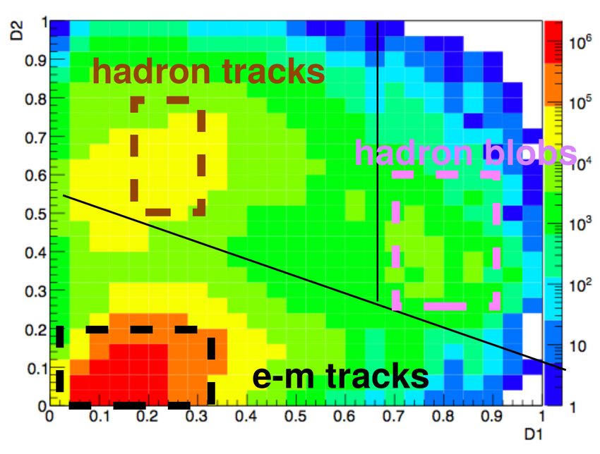
with high spacial and energy resolution are required. The development of such detectors
nowadays is largely based on the experience gained in nuclear physics and high energy
physics.
Joint Institute for Nuclear Research and, in particular, Laboratory of Nuclear Prob-
lems have a rich history of methodical research and development of a wide variety of
detectors. Moreover, we can safely say that the Laboratory owes its most striking physi-
cal results to the scienti
c and methodical studies conducted beforehand. This statement
applies not only to the experiments carried out at JINR, but, to a less degree, also to the
visiting experiments at accelerators of other centers. The proposed Project aims to create
in the DLNP a research infrastructure for conducting scienti
c and methodical studies
on the development of new types of semiconductor detectors for accelerators experiments.
Since these detectors can be successfully used in applied research in other
elds of science,
an important component of the proposed Project is to create a working scheme for joint
interdisciplinary applied studies and for implementation of the results in innovative
elds
of the economy of the member states.
For a long time semiconductor detectors have been used as sensitive elements of co-
ordinate and calorimeter subsystems of various experimental installations that combine
high readout speed with high spatial and energy resolution. However, the requirements
for the planned detectors of the next generation of experiments (for ILC, CLIC, HL-LHC,
the muon collider, etc.) are considerably higher than the characteristics of semiconductor
detectors achieved today. To ful
ll those requirements additional research and develop-
ment in the
eld of semiconductor detectors is needed. The list of necessary improvements
includes higher readout speed, higher degree of segmentation and, more importantly, a
cheaper price tag, since we are talking about large installations with hundreds or thou-
sands of individual detecting elements. However, in contrast to the LEP7 , Tevatron and
LHC8 experiments, on the top of the requirement list is radiation hardness because of
much longer life cycles and much higher luminosities of the planned future accelerators in
comparison to the existing accelerator complexes.
Modernization of the LHC experiments for the Phase-2 stage and detector projects for
the ILC experiments impose the dose of ionizing radiation up to 1 MGy and non-ionizing
radiation
uence up to 2 · 1016 MeV·n/cm2 [7]. All existing silicon detectors become inop-
erative after accumulation of a dose smaller by an order of magnitude. The only known
method for operation of silicon detectors under such radiation load is reducing of the op-
erating temperature down to several tens of degrees. However, this method signi
cantly
complicates the design of the detector and raises intractable requirements on the detector
7 Large Electron-Positron collider
8 Large Hadron Collider
4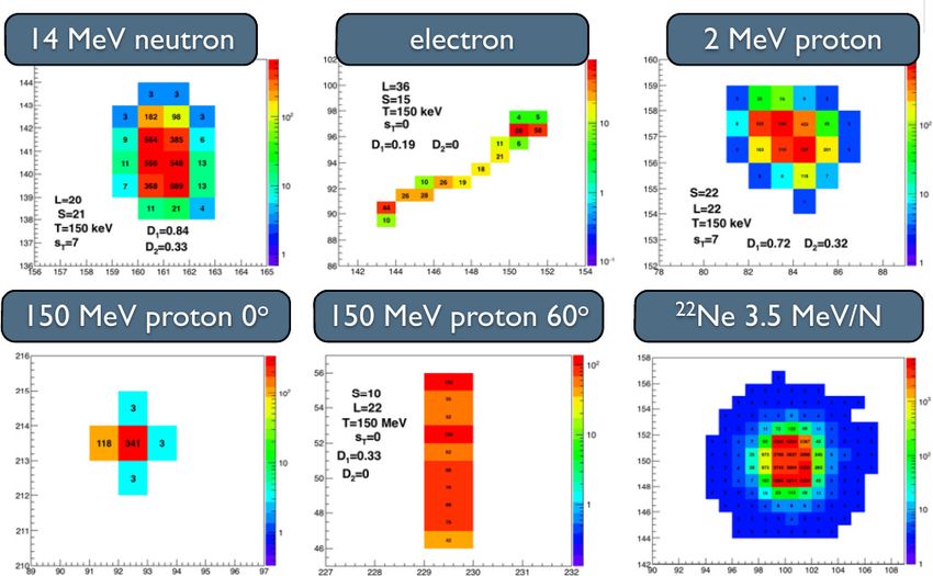
heat output. The last requirement is particularly important since the high load on the de-
tector implies a complex trigger system that require rather complicated signal processing
directly in the detector, including time measurements, clusters recognition and measure-
ment of correlations between signals in adjacent pixels. The only alternative to frequent,
time-consuming and costly replacement of detecting elements damaged by radiation in
the current day installations is development of a new generation of radiation-resistant
detectors, based on modern technological advances and the use of new materials.
Developments in the
eld of semiconductor detectors is largely determined by techno-
logical advances in industry. Nowadays, practically none of the research institutes grows
silicon crystals or manufactures readout chips for its needs in high-energy physics because
it is much easier and cheaper to do at the enterprises of the microelectronic industry.
In most research centers for high-energy physics the emphasis shifted from the actual
production of detectors to making speci
cations for detectors, to design and assembly of
prototypes or sometimes small-scale batches of detectors from commercially produced el-
ements. The most important stage in the development cycle of new detectors is the study
of their characteristics, which provides feedback to the manufacturer of sensitive elements.
The study of detector characteristics includes both the control of correspondence of the
basic detector properties to its speci
cations and direct evaluation of the sensor detecting
properties. The key tests for new detectors are tests on beams of dierent elementary
particles that allow studies of the detector properties in conditions close to operational.
Regarding the evaluation of detector radiation hardness, these tests are the most impor-
tant. In this respect JINR has a great advantage, because it possesses a large number of
installations that allow testing of detectors in beams of dierent particles, from protons
and neutrons to heavy ions. The close scienti
c relations with almost all world centers of
high-energy physics allow, if necessary, to carry out such beam tests at any accelerator in
the world.
Development of semiconductor detectors based on a new radiation-resistant material
- modi
ed gallium arsenide produced by Tomsk State University (TSU) - has been con-
ducted in the LNP since 2006. In the course of this development scienti
c relations with
the world's centers performing similar studies were established, a number of joint research
projects with TSU to create a sensor with the desired properties were carried out, con-
siderable experience in the production and operation of such detectors (in pad and pixel
geometry) was accumulated, the detector characteristics were measured. The obtained ex-
perience allows to move to more complicated tasks and to pursue developments in several
directions simultaneously. The following tasks form the basis of the proposed Project:
1. Development of the existing scienti
c and technical groundwork for design and de-
velopment of semiconductor radiation-resistant detectors based on new materials
5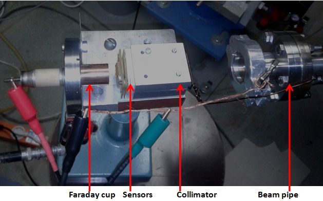
and hybrid pixel detectors with high resolution for accelerator experiments. In the
future - the development of some of the necessary, but currently lacking, facilities in
the LNP: for mechanical and chemical processing of semiconductors, for assembly
of pixel detectors and for design of readout electronics.
2. Improvement of the existing and development of new testing stations for measuring
properties of detectors produced at JINR and at laboratories of JINR member states,
coupled with beam tests at the specialized JINR facilities.
3. Joint scienti
c work in collaboration with research groups from other institutes in
feasibility studies of application of the newly developed detectors in other areas of
science and technology (primarily in the
elds of medicine and geology), in partic-
ular, applications for the MARS microtomograph that uses the new sensors with
modern readout electronics based on the Medipix chip.
In the following chapters the main results obtained during the implementation of the
2015-2017 Project for each of the tasks are presented alongside with the proposed work
plan for 2018-2020.
6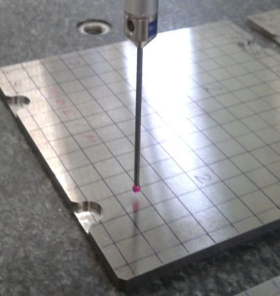
Chapter 2
Investigations of semiconductor detectors for
nuclear physics and particle physics
The basis of operation of semiconductor detectors is the formation of non-equilibrium
charge carriers (electrons and holes) during passage of an ionizing particle. If an electric
eld is applied to the semiconductor the drift of the non-equilibrium charge carriers gen-
erates a current pulse in the detector circuit, which can be ampli
ed and recorded. Silicon
and germanium are traditionally used for the production of semiconductor detectors, with
the latter mainly being used in precision spectroscopy. Of great interest are other semi-
conductor materials suitable for making detectors, such as CVD-diamond, silicon carbide,
gallium nitride and gallium arsenide.
The latter material is especially interesting because it has long been used successfully
in the microelectronic industry in manufacturing of devices and integrated circuits for
ultra-high-speed and microwave electronics. In this regard, there exist in the world in-
dustrial technologies for the production of gallium arsenide and its properties have been
thoroughly studied. In world practice, semi-insulating gallium arsenide (LEC-GaAs) is
commonly used. However, this type of gallium arsenide has signi
cant drawbacks that
limit its use as a material for the production of particle detectors. The main problem is
the impossibility of creating a detector material with a low content of impurities. As a
result, the maximum depth of penetration of the electric
eld in the sample is 200 - 250
µm, which limits the thickness of the sensitive layer of LEC SI-GaAs structures. Conse-
quently, despite numerous attempts in the world, until recently it has not been possible
to create semiconductor detectors of ionizing radiation of good quality on the basis of
semi-insulating gallium arsenide.
Progress in recent years in the creation of such detector material is associated with the
work of the Tomsk scienti
c school under the leadership of O. P. Tolbanov, a professor at
Tomsk State University. The technology for compensation of n-type conductivity in LEC
7GaAs layers in the process of thermal diusion of deep acceptor impurity of chromium
(GaAs:Cr) was developed. The experimental values of the resistivity of such structures are
measured to be about 109 Ohm·cm, which is by more than an order of magnitude greater
than the resistance of structures based on LEC SI-GaAs. This implies the transition from
barrier-type structures to structures of resistive type. Ohmic contacts can be formed to
such structures that allows for a uniform distribution of the electric
eld strength over
the entire thickness of the detector. To date, samples of chromium compensated gallium
arsenide with a thickness of the sensitive layer up to 1 mm have been obtained at TSU [12].
One of the most complex technical issues in creating a semiconductor detector is
readout of the signal. If for a pad or micro-strip detector the readout can be made
relatively easily, for a pixel detector the signal readout is a much more complex problem.
When the size of an individual pixel is reduced to hundreds or tens of microns and
the total number of pixels reaches thousands or tens of thousands, there is no other
ways besides developing of a specialized readout chip containing the required number of
channels of electronics. Thus, we obtain a hybrid pixel detectors consisting of a sensitive
layer (sensor) made of a single crystal semiconductor and a readout chip, interconnected
by bump-bonding (Figure 1).
Figure 1: Typical scheme of a hybrid pixel detector.
The conventional electronics used to readout signals from pixel detectors amplify the
electrical signal
rst and then integrate it to determine the amount of the collected charge.
It implies that the intrinsic noise of the sensor is inevitably added to the signal, that leads
to a deterioration in image quality and a decrease in the energy resolution. However,
over the past 10 years advances in microelectronics have made it possible to implement a
fundamentally new approach, in which the spectrometric circuit is assembled directly in
a single pixel. It allows to carry out not only ampli
cation, but also amplitude discrimi-
nation and digitization of the signal in the pixel. The high readout speed of such circuits
8makes possible to be performed these operations independently for each particle. The
output signal in this way is digital, namely, the number of particles with energy above a
predetermined threshold set by the discriminator, instead of an analog signal proportional
to the collected charge. This approach has been called the single photon counting mode,
since it was
rst implemented for photodetectors.
The development of such readout microcircuits is carried out by three groups: in PSI
(Switzerland, PILATUS [14] family of chips), CPPM-IN2P3 (France, XPAD [15] family
of chips) and MEDIPIX collaboration (CERN, Medipix2, Timepix, Medipix3 [16] chips).
In terms of their characteristics (the size and number of pixels, capabilities of readout
electronics), the Medipix family of chips outperform the analogues developed by the other
two groups.
2.1 Main results in 2015-2017
2.1.1 Investigation of radiation hardness of detectors based on gallium ar-
senide
The radiation hardness of LEC gallium arsenide has been studied some time ago by the
RD8 experiment at CERN [9]. It has been shown that detectors made of uncompensated
gallium arsenide can withstand a
uence of 3 · 1014 protons, 2 · 1014 pions and 6 · 1014
neutrons per cm2 . For compensated semi-insulating gallium arsenide a similar radiation
hardness was determined, and also it was shown that the dose of 100 kGy accumulated
during irradiation by photons with energy of 660 keV leads only to a slight deterioration
of the detection properties [10]. Studies conducted by irradiating GaAs detectors with
1.17 and 1.33 MeV gamma rays from a 60 Co radioactive source did not show signi
cant
radiation damage up to the accumulated dose of 1 MGy [11]. Radiation tests of GaAs:Cr
pad detectors made at JINR, which were carried out within the framework of the FCAL
collaboration on an electron beam with an energy of 8.5-10 MeV on the S-DALINAC
accelerator in Darmstadt, showed that the detectors remain operational until the accu-
mulated dose of 1.5 MGy [13]. Although it was shown that the compensated gallium
arsenide is quite a promising material for high radiation resistant detectors, until recently
systematic measurements of radiation hardness of GaAs:Cr detectors in comparison with
silicon detectors were absent, as well as studies with neutron beams. In addition, studies
of radiation hardness of barrier πν -structures on electron beams have never been carried
out at all.
In the framework of this Project, in the autumn of 2016, systematic tests of radiation
hardness of 2 types of gallium arsenide pad detectors (barrier πν -structures and highly
9Figure 2: The output beam-line of the Linac-200 accelerator and the setup for irradiating
pad sensors.
resistive structures) and n-type silicon detectors on an electron beam with an energy of
20 MeV were conducted. The tests were carried out at the LINAC-200 accelerator at
JINR (Figure 2). The detectors with an area of 5 mm × 5 mm were irradiated in steps
of dose from 50 kGy to 200 kGy until a total absorbed dose of 1.5 MGy was achieved.
After each step, the current-voltage characteristic and the charge collection e
ciency at
room temperature were measured.
As a result of the tests, it was shown that the radiation damage aects the performance
of the silicon and gallium arsenide detectors in dierent ways. Silicon is characterized by
a rapid increase in the dark current, up to 4 orders of magnitude when irradiated with a
dose of 1.5 MGy. This makes impossible usage of silicon detectors without cooling under
irradiation with a dose of more than 0.5 MGy, although the charge collection e
ciency
remains constantly high. As for GaAs:Cr, the dark current increases moderately, three
times for resistive material and 4-5 times for barrier structures. However, gallium arsenide
is characterized by a decrease in the e
ciency of charge collection. It should be noted
that the charge collection e
ciency in GaAs:Cr decreases sharply (by a factor of 5) when
irradiated with a dose of 0.5 MGy, and then continues to decrease slowly with a further
increase in dose, remaining at a level of 10% at a dose of 1.5 MGy, which is quite su
cient
for the detector to be operational. The curves of the current-voltage characteristics, charge
collection e
ciency, and examples of spectra are shown in Figure 3,4,5, respectively.
Similar results were obtained by irradiation with neutrons in the beams of the IBR-2M
reactor (Figure6). The tests were carried out in November 2016 for two types of detectors
based on GaAs:Cr and one n-type silicon detector, with three values of
uence: 5.5·1011 ,
2·1012 , and 4.5·1013 n/cm2
10Figure 3: Current-voltage characteristics of detectors after irradiation. The upper row
are gallium arsenide detectors (resistive structures on the left, barrier structures on the
right), the lower row are silicon detectors (n-type silicon detectors from USCS (USA) on
the left, the detectors provided by N. I. Zamyatin's group on the right).
Figure 4: Dependence of the charge collection e
ciency on the absorbed dose. Left -
gallium arsenide detectors, right - silicon detectors.
11Figure 5: The spectra obtained on gallium arsenide (left) and silicon (right) detectors
after irradiation with a dose of 0.5 MGy, at room temperature.
Figure 6: Dependence of the relative e
ciency of charge collection on neutron
uence for
silicon and gallium arsenide detectors.
122.1.2 Development of FCAL calorimeter for future electron-positron collid-
ers
Preparing for future experiments at high luminosity electron-positron colliders (ILC,
CLIC, FCC, CEPC) required additional research in order to develop special calorime-
ters for the forward region. These calorimeters should be compact, have a high spatial
resolution for the separation of showers, high positioning precision and high speed. Since
detectors in the forward region are subject to very high radiation load, they must have an
unprecedented radiation hardness. Depending on the angular aperture and the performed
task, several calorimeters are distinguished: Pair Monitor, BeamCal, LumiCal [17, 18].
The BeamCal calorimeter is the closest to the beam pipe, and accordingly, is subject to the
greatest radiation load. It is designed to measure large amount of soft electron-positron
pairs produced by the conversion of bremsstrahlung, and high-energy beam electrons to
facilitate adjustment of the beam parameters. Development of these detectors is con-
ducted by the FCAL international collaboration. To achieve the required characteristics,
a compact sandwich calorimeter with a high degree of segmentation consisting of tungsten
absorber and recording planes made of semiconductor detectors has been proposed.
In addition to studies of the radiation hardness of detectors based on gallium arsenide
that are necessary for selection of the optimal material for the sensitive element of the
compact sandwich calorimeter FCAL, some work on the production of tungsten absorber
plates for a full-scale prototype of the calorimeter module was carried out at JINR. The
main di
culty lies in the extremely high requirements for the
atness of the plates
less than 20 microns for the
nal version of the calorimeter. In 2015-2016, orders were
placed for the production of trial batches of tungsten plates from two Russian suppliers
and geometric parameters of the manufactured plates were measured using a three-axis
coordinate measuring machine Zeiss Eclipse installed in a clean room at the NEOVP
DLNP JINR (Figure 7).
In total, 5 tungsten plates were produced by one supplier and 2 plates by another
supplier. For quality control, a measurement technique has been developed that makes it
possible to achieve repeatability of the results within the range of 1.5-2 µm. As a result
of the measurements, one vendor was selected who managed to ensure
atness within 35
µm (Figure 8), which is quite enough to produce a prototype of the forward calorimeter
module. During 2017-2019, production and delivery for the FCAL collaboration of about
30 tungsten absorber plates are planned.
13Figure 7: Measurement of the geometric parameters of the FCAL tungsten absorber plates
using Zeiss Eclipse three-axis coordinate measuring machine.
2.1.3 X-ray imaging detectors of large area
The use of hybrid pixel detectors makes a revolution in the
eld of detecting photons
from synchrotron radiation sources and from sources on X-ray free electron lasers. By
all accounts, they are detectors of the future, as they give a signi
cant improvement in
image quality compared to current detectors based on CCD cameras. Examples are the
large area detectors based on the readout chips Pilatus, Medipix and XPad, developed by
various institutes in Europe. Due to commissioning of new sources of high-energy X-ray
radiation, the demand for e
cient material for sensors has grown rapidly over the last
ve years. The most promising materials for this region of X-ray energies are GaAs and
Cd(Zn)Te. The medical imaging industry invests mainly in Cd(Zn)Te, since their main
applications (human scanning) require high photon energies above 100 keV, which in turn
requires sensors from high Z material. Synchrotron radiation sources have a large and
growing emphasis on energy in the range up to 80 keV, for which GaAs is best suited.
As a continuation of the successful project GALAPAD (2011-2013) to develop a tech-
nology for the production of GaAs hybrid pixel detectors of the Hexa type (assem-
bling 3×2 Medipix chips on a common sensor), in 2014 the joint Russian-German project
GALAPAD-2 was started. The project aims to develop large area pixel detectors of the
Double-Hexa type (assembly of 6×2 chips) with the area of the active region of 82×28
mm2 . This project involves JINR (with TSU as a co-executor) from the Russain side and
DESY, the Karlsruhe Institute of Technology and the Freiburg Materials Research Center
14Figure 8: Results of measuring of the surface shape of the tungsten absorber plates for
FCAL. The distance to the surface of the plate in mm is shown relative to the base plane
for the two sides of the absorber plate.
from the German side. The project was supported by the Russian Ministry of Education
and Science within the framework of the Federal Program "Research and development
in priority areas for the development of Russia's scienti
c and technological complex for
2014-2020", with a funding volume of 47 million rubles in 2014-20171 .
To ful
ll this project, it is required to develop a technology for production of gallium
arsenide sensor wafers of 400 size, to develop methods for controlling the sensors quality,
to improve the technology of mounting readout chips on a common sensor and to develop
high-rate electronics for data acquisition. The detectors will have much reduced insensitive
area at the edges of the sensor, which will allow to tile such detectors on four sides and use
them as elements of detecting systems of arbitrarily large area. The detector modules will
be tested on the synchrotron sources ANKA in KIT and PETRA-III in DESY. Additional
experiments will be carried out to evaluate GaAs as a material for detectors for X-ray
free electron lasers in particular, the ability of GaAs detectors to withstand a high
instantaneous
ux appearing at high intensity radiation sources.
In the course of carrying out the GALAPAD-2 project, the following main results were
obtained at JINR in cooperation with TSU:
• in JINR a modern test bench based on the Cascade Microtech EPS150TESLA probe
station for studying properties of semiconductor materials has been created and put
into operation;
1 Agreement on granting subsidies from the Russian Ministry of Education and Science of September
17, 2014, No. 14.618.21.0001.
15Figure 9: The
rst batch of GaAs:Cr sensor wafers with a diameter of 102 mm, produced
within the GALAPAD-2 project.
• in TSU 40 sensor wafers with a diameter of 76 mm (one sensor of Hexa size on each
wafer) made of modi
ed gallium arsenide GaAs:Cr were manufactured for testing
the dicing technology for a reduced size of the insensitive region at the sensor edges
(slim-edge technology). At JINR, a visual inspection of the obtained sensor wafers
was carried out under the microscope: eleven out of the forty wafers had either
defects in metallization or mechanical damage. The characteristics of all the sensor
wafers were measured on the probe station in order to discard wafers that were not
suitable for subsequent use as sensors in hybrid pixel detectors;
• in TSU the technology of production of sensor wafers with a diameter of 102 mm
from compensated gallium arsenide has been mastered, 17 sensor wafers of the
Double-Hexa size have been manufactured to this day (Figure 9);
• JINR has become a full member of the Medipix-4 international collaboration;
• JINR
led patent Application No. 2016150633 dated December 22, 2016 for the
invention Semiconductor Matrix Detector for Charged Strongly Ionizing Particles
(Multiply Charged Ions) and patent studies were carried out.
In Germany, the technology of simultaneous bonding of 12 readout chips with a com-
mon sensor and the technology of dicing slim-edge sensors are being worked on, as well
16as the development of a high-speed Lambda data acquision module with a rate of 1000
frames per second. After completion of the work, one of the Lambda detector modules
with a Double-Hexa sensor will be delivered to JINR.
The GALAPAD-2 project should be completed by the end of 2017.
During the year 2015, in addition to cooperation within the GALAPAD-2 project, 50
pixel sensors each with an area of 28×42 mm2 (with the total area of about 600 cm2 ),
required to create a large area pixel detector to be used on the XFEL beamlines, were
fabricated and tested within the framework of a separate collaboration between JINR-
DESY-TSU.
2.1.4 Hybrid pixel detectors based on the Timepix readout chip
Development of the procedure for per-pixel energy calibration of Timepix detectors
For energy calibration of Timepix detectors with GaAs:Cr sensors, a per-pixel calibration
procedure was developed that uses characteristic lines in the X-ray spectra of various met-
als, which were accurately measured beforehand by a spectrometer based on germanium
detector (LEGe Canberra GL0515R). The main advantage of using X-ray characteristic
radiation is the high speed of acquiring the necessary set of data (the procedure can be
repeated using a set of reference radioactive γ -sources, but the data collection time is
increased by an order of magnitude).
Thanks to the use of per-pixel calibration, it was possible to achieve a good energy
resolution of Timepix detectors with GaAs:Cr sensors: 8.5% at 59 keV. It was shown that
further improvement in the calibration quality in the low-energy part of the spectrum
(5-15 keV) can be achieved by increasing the number of reference points which are used in
the
tting of the calibration curve in this region. Providing that the spread of parameters
of detectors based on the Timepix chip is small, i.e. detectors give similar ToT2 spectra
with the same settings of the DAC and at a stabilized temperature of the sensor, the
per-pixel calibration of the detectors can be carried out in the almost automated mode.
To accomplish this task, special software has been developed. This feature is especially
relevant for installations with a large number of Timepix detectors.
Investigation of Timepix pixel detector with 1 mm thick gallium arsenide sensor
In 2015, the
rst Timepix detector with a 1 mm thick gallium arsenide sensor was man-
ufactured at JINR in cooperation with TSU and CTU (Prague). The assembly quality
2 Time-over-Threshold the duration of the signal above the threshold, proportional to the energy
deposited in the sensor.
17Figure 10: General view and energy resolution of the Timepix detector with 1 mm thick
gallium arsenide sensor.
was very high (99.9% of usable pixels). As a data acquisition system we used the RelaxD3
chip-board. The per-pixel energy calibration was performed according to the method de-
veloped at JINR. The energy resolution of the detector is 12% at 20 keV and 7% at 60
keV (Figure10). The accuracy of the energy scale is better than 1% for gamma quanta
with energies below 100 keV. Figure 11 shows the emission spectrum of the 137 Cs source
measured by this detector. One can see that the energy resolution is 4.8% at 660 keV.
Investigation of long-term stability
In mid-2015, the program to measure the long-term stability of Timepix detectors with
gallium arsenide sensors was started. The measurements were made as follows. A standard
radioactive source of 241 Am was placed at a distance of 1 cm from the surface of a Timepix
detector. Measurements of the energy spectrum of the source continued throughout the
year, while analyzing changes in the position of the photopeak at 59 keV, determined for
both all the pixels as a whole and for several separate zones of the sensor. It was shown
that the position of the photopeak moved during the year by less than 1 ppm (Figure 12).
Simultaneous recording of the temperature allowed to conduct parallel measurements of
the temperature dependence of the detector response (Figure 13). The obtained results
lead to the conclusion that the spectrometric capabilities of the Timepix gallium arsenide
detector are highly stable.
3 Manufacturer - Amsterdam Scienti
c Instruments, The Netherlands.
18Figure 11: Spectrum of 137 Cs after the per-pixel energy calibration of the Timepix detector
with 1 mm thick gallium arsenide sensor.
Figure 12: Change in the position of the 59 keV photopeak of an 241
Am source as a
function of time.
19Figure 13: Stability of the position of the 59 keV photopeak of an 241 Am source at dierent
temperatures.
20Measurement of sensor transport characteristics in a pixel detector
An important characteristic that determines the collection of charges in a semiconductor
detector is the product of the lifetime of nonequilibrium carriers τ by their mobility µ. In
the course of the project, a method for determining µτ of electrons in gallium arsenide
for pixel detectors was developed, based on the use of a beta separator (a source of
monoenergetic electrons). The operation of the beta-separator is based on selection of
a given energy from a wide spectrum of β -electrons formed in the radioactive decay of
90
Sr with the help of an electron collimator. The obtained dependences are shown in
Table 2.1. It should be noted that the ability to reliably detect a signal from electrons
with an energy of 100 keV shows that in gallium arsenide the thickness of the `dead 'layer
is not more than 24 µm - the mean free path of electrons of this energy.
Table 2.1: Changes of the µτ value with the varying thickness of the sensor. The electrons
penetration depth is determined by their energy.
The use of X-ray
uorescence on zirconium foil makes it possible to measure µτ sepa-
rately for each pixel. For 15.7 keV gamma-ray (the Kα line of zirconium) the attenuation
length in gallium arsenide is less than 25 µm, which suggests that most of the interactions
occur directly near the cathode. Measuring the dependence of the photopeak position
on the bias voltage for each pixel and approximating it with the Hecht curve one can
determine the value of µτ [23]. The results are shown in Figure 14. The average value
of the product µτ for electrons in the gallium arsenide sensor is 1.1·10−4 cm2 /V with the
variance of 1.5·10−5 cm2 /V.
Studies of pixel detector response with synchrotron radiation
In 2016 several measurements with hybrid pixel detectors were performed on the syn-
chrotron radiation beamline of the VEPP-3M accelerator (Budker Institute of Nuclear
Physics, Novosibirsk). This allowed us to experimentally investigate the behavior of gal-
lium arsenide pixel detectors at high loads, as well as measure characteristics of the detec-
tor in the Medipix mode (counting individual photons) using a collimated monochromatic
21Figure 14: The value of µτ depending on the pixel position (left); distribution of the µτ
values for all pixels in the detector.
X-ray beam. The experiment was carried out at the synchrotron station Tomography
and microscopy with monochromatic photons, whose energy varied in the range of 6-40
keV with the spread of dE/E = 0.072%. The use of the collimator made it possible to
obtain a parallel beam with a transverse size of 10 µm × 10 µm. Precise positioning of
the detector allowed to direct the beam to the desired part of the pixel.
The dependence of the energy resolution of the detector on the photon energy is
shown in Figure 15 for three cases: for the photons hitting the geometric center of a pixel,
averaged over all photons for the detectors with a sensor of 300 µm and 900 µm thickness.
The best result of 4.5% at 18 keV is achieved for the photons hitting the center of the
pixel.
2.1.5 Pixel detectors as elements of tracking systems
Pixel silicon detectors are a promising tool for creating tracking systems which are already
actively used in high energy physics. One of possible applications is the investigation of
the electromagnetic dissociation of the carbon isotope 9 C, namely, determination of the
probability of its fragmentation into three 3 He. The VBLHEP has prepared a rig for the
telescope made of 4 silicon detectors based on the Timepix chip. In this setup the
rst
detector is rotated almost parallel to the beam, therefore it serves simultaneously as a
tracking detector and a target. With such a rotation angle, incoming particles are visible
and 9 C can be identi
ed, the interaction point and outgoing tracks are visible too. In
the VBLHEP experiments, the cross section of the interaction of carbon with silicon was
22Figure 15: The dependence of the energy resolution of the detector (expressed as a per-
centage of the measured energy) on the photon energy.
measured, so one can expect one interaction in such a detector per 1000 incoming particles.
The main tasks of this activity are mastering the technique of working with detectors,
studying the Coulomb dissociation of radioactive nuclei and their fragmentation. The
accuracy of track reconstruction in the telescope depends on the shape of the cluster and
can reach 2-3 microns. It should be noted that with the help of this method it is possible
to study a number of processes which earlier were possible to study only with the help
of photoemulsions. The main limiting factor hindering the use of the telescope in this
experiment is the low rate of the readout electronics, so it is highly desirable to replace
the electronics with a faster one.
In the course of the Project, Timepix detectors were tested on a beam of 12 C carbon
nuclei with an energy of 1.2 GeV/nucleon at the JINR Nuclotron. Distributions of cluster
sizes and energy losses were obtained. A relative equalization of Timepix detectors in the
telescope has been carried out. The measurement of the number of δ -electrons on the
length of the Timepix detector showed that the methods used to determine the nuclear
charge by the number of δ -electrons in photoemulsions can not be directly transferred to
pixel detectors and need to be modi
ed.
23This work is carried out in cooperation with a group from the Czech Technical Uni-
versity (Prague).
2.2 Research program for 2018-2020
2.2.1 Searches for methods to increase the radiation hardness of gallium
arsenide detectors
The obtained in 2016 measurement data on the radiation hardness of detectors will be used
to develop a GaAs:Cr radiation damage model and, in the future, to
nd ways to increase
their resistance to irradiation. The main reason for the deterioration of detector properties
of gallium arsenide is the formation of defects in the crystal lattice, with dierent types
of irradiation leading to dierent types of defects and dierent rate of their appearance.
As measures to increase radiation hardness, the introduction of doping impurities that
compensate for the eect of defects on charge collection is usually considered. Since this
method (chromium compensation) is the basis for the production of high-resistive gallium
arsenide, there is a certain hope of increasing the radiation hardness of this material by
changing the chromium compensation technology or introducing additional impurities.
However, this requires quantitative measurements of the rate of formation of various
types of defects for dierent types of irradiation and dose rate. The existing measurement
methods current-voltage and capacitance-voltage characteristics, the charge collection
e
ciency of course, give certain information, but do not allow us to distinguish the
types of defects that are formed. To solve this problem, it is planned to establish at
DLNP during 2018-2019 a station for carrying out measurements using the methods of
deep level transient spectroscopy (DLTS).
When these studies are performed, additional irradiation sessions of samples are
planned on the electron beam of the Linac-200 accelerator, the neutron beams of the
IBR-2M reactor, and possibly other sources of radiation.
These works will be carried out in cooperation with TSU and the Institute for Space
Research (Bucharest-Magurele, Romania).
2.2.2 Identi
cation of particles in hybrid pixel detectors
Dierences in the nature of interactions of charged particles of dierent types with matter
(dierent path, scattering probability, amount of energy released) lead to a visible dier-
ence in the shape of the clusters and the magnitude of the signal on the pixel detectors
(Figure 16). These dierences can be used to identify particles by their response.
24Figure 16: Typical clusters formed in Timepix detectors by dierent types of particles.
In the course of the Project, many data runs were conducted with the Timepix detector
on the beams of dierent JINR and CERN facilities for dierent types of particles: X-ray
and high-energy gamma quanta, electrons, protons, alpha particles, neutrons, deuterons
and heavy ions of various energies. As a result, a new method of particle identi
cation
was developed to separate interactions having electromagnetic or nuclear nature. For
separation, two parameters D1 and D2 are used. The parameter D1 is calculated as the
ratio of the cluster area to its perimeter and characterizes the shape of the cluster. The
parameter D2 is calculated as the number of pixels with energy release above a certain
threshold to the total number of pixels in the cluster and characterizes the ionization
losses of particles. An example of the separation is shown in Figure 17.
During the implementation of the Project in 2018-2020, it is planned to improve the
procedure for particle identi
cation and to obtain numerical estimates of the e
ciency
and purity of the obtained separation.
2.2.3 Neutron registration
Detection of neutrons and determination of their spectrum with the help of Timepix
detectors have great practical importance. Although in the case of thermal neutrons
the possibility of recording them using various converters has been successfully demon-
25Figure 17: Separation of cluster types in the Timepix detector based on parameters D1
and D2.
strated [20, 24, 25], registration and determination of the fast neutron spectrum is a more
di
cult task.
In the fall of 2015, during the course of the Project, the response of a Timepix detector
to neutrons was investigated on a neutron beam of the n_TOF facility in CERN. Detectors
with a sensor made of silicon and gallium arsenide were irradiated with neutrons with
energies from 1 eV to 1 MeV. Using the time-of-
ight information, the neutron spectrum
recorded by these detectors was reconstructed (Figure 18). To do this, Timepix detectors
were set to work in mixed mode (every 9th pixel measured not the amplitude of the signal,
but the time from the beginning of the signal to the end of the frame).
During 2018-2020, it is planned to carry out additional measurements and experi-
mentally determine the dependence of neutron detection e
ciency of gallium arsenide
detectors on neutron energy, and also to study the use of several converters with dierent
neutron-induced thresholds for determination of the fast neutron spectrum.
The results of this work will be especially useful when analyzing and interpreting data
coming from the GaAsPix [26] radiation background monitoring system installed in the
26Figure 18: Spectrum of neutrons in Timepix detectors with sensors from silicon and
gallium arsenide.
ATLAS cavern at the LHC.
2.2.4 Studies of hybrid pixel detectors response to the passage of heavy
charged particles
Although the response of Timepix silicon detectors to the passage of heavy ions was
studied by several groups [27, 28], up to now there was no information on the response
to heavy ions of similar detectors with a gallium arsenide sensor. In particular, the use
of Timepix silicon detectors for detecting heavy ions has shown the presence of the so-
called volcano eect - deformation of the cluster pro
le in the region of maximum energy
release (Figure 19).
During the implementation of the Project, a series of measurements was carried out
on the beams of the U-400M FLNR accelerator, in which Timepix detectors with silicon
and gallium arsenide sensors were irradiated with various heavy ions at dierent beam
energies. As a result of these measurements, it was shown that there is no volcano
27Figure 19: Volcano eect in the silicon (left) and gallium arsenide (right) Timepix
detectors when irradiated with Ne ions with an energy of 158 MeV.
eect in gallium arsenide detectors (Figure 19), but there is a large non-linearity in the
measurement of energy, related both to the saturation of the readout preampli
er and to
physical processes in the sensor itself. This makes di
cult calibration of the detectors
and complicates accurate measurements of the ion energy.
During 2018-2020, it is planned to study in detail the mechanism of the formation of the
Medipix detector response to the passage of heavy charged particles releasing high energy
and to develop reliable methods for measuring the energy and coordinates of particle
interaction. It should be noted that the large cluster size (several dozen simultaneously
triggered pixels) allows to signi
cantly increase the spatial resolution of the detector by
nding the center of gravity of the pixels in the cluster.
Development and veri
cation of the methods for determining characteristics (intensity,
pro
le, particle composition) of heavy ion beams using the Medipix detector in the energy
range from 5 keV to 10 MeV per nucleon will be useful for the creation of heavy ion beam
diagnostic equipment, in particular, for measuring the energy of the incident beam and
for the creation of positionally sensitive detectors for monitoring and visualization of the
pro
le of a heavy ion beam.
2.2.5 Application of pixel detectors in experiments with hypernuclei and
relativistic ions on the Nuclotron
For experiments on the Nuclotron, a new polarimeter for the source of polarized deuterons
is needed. The polarization of the beam should be measured both directly behind the
linear accelerator LU-20 and in the Nuclotron ring. The polarization is measured by
determining the left-right asymmetry in the scattering of ions at a given angle. It is
28proposed to use the Timepix detector as a sensitive element of the new polarimeter. The
intensity of scattered particles is of the order of 100 Hz, which is quite acceptable for such
a detector. Compared to the existing electronics, which can only work at a
ow rate of
no more than 10 Hz, the new system will allow to reduce the measurement time by an
order of magnitude and simultaneously improve the accuracy due to the higher spatial
resolution of the Timepix matrix. A new polarimeter based on the Timepix detector is
planned to be manufactured and installed during 2017-2019.
29Chapter 3
Research infrastructure in the DLNP of JINR
3.1 Main results in 2015-2017
3.1.1 Kalan measuring station
The Kalan measuring station is designed for detector calibration and for studies of
the response of detectors using X-rays and, in the future, closed radioactive sources.
The station consists of an X-ray protected locker equipped with an automatic switch-
o system when the doors are opened, in which the radiation source and the detector
under investigation are connected to a data acquisition system and a high voltage supply
(Figure 20). Microfocus X-ray tubes RAP-150MN or SourceRay SB-120 with operating
voltage up to 150 and 120 kV, respectively, controlled by a PC are used as a source of
radiation, alongside with radioactive sources.
3.1.2 Testing bench based on a probe station
In 2015, a testing bench based on the Cascade Microtech EPS150TESLA probe station
was developed and put into operation for studying properties of semiconductor materials.
Preliminary renovation work was done in the clean room where the test station was
installed: the
oor was reinforced, the ventilation system was updated, compressed air
and vacuum systems were cleaned, and the grounding loop was improved. These measures
are needed to ensure stability of the necessary environmental conditions in the clean
room for the normal operation of the probe station. In the clean room a metal frame on
two concrete supports was installed, covered with a 5 mm steel sheet, as a base for the
probe station mounting. All components of the testing bench (the probe station itself,
the module for high voltage supply, the Keithley 2400 picoamperemeter, the Keysight
(Agilent) E4981 capacitance meter, the temperature regulator) were installed during the
30Figure 20: Kalan measuring station.
year 2015. Figure 21 shows the general view of the created test bench.
The testing bench allows to measure the current-voltage and capacitance-voltage char-
acteristics of the samples under study in patches up to 5 µm × 5 µm in size. The range
of the measured currents is from 0.1 nA to 100 mA at a bias voltage up to 1 kV with the
measurement accuracy being better than 5
3.1.3 Station for measuring charge collection e
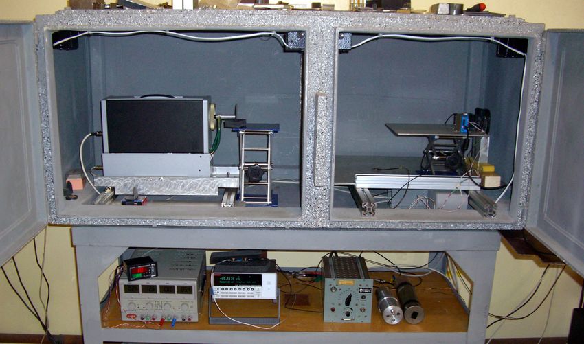
ciency
To measure the e
ciency of charge collection, a special station was designed and created.
The operation of the station is based on the passage of a collimated electron beam from
a radioactive β -source 90 Sr with subsequent acquisition and analysis of the signal in the
detector under investigation using the DRS4 module. Trigger signal is formed on the
basis of the response of two scintillation counters, that allow to measure the e
ciency
of charge collection up to extremely low values (less than 1%) due to suppression of
background random triggers. At the same station, it is possible to measure the current-
voltage characteristics of the detector. Measurements are quite fast: the measurement
time of charge collection e
ciencies is usually about 15 minutes, the time for determining
current-voltage characteristics is about 10 minutes. On the station it is possible to perform
characterisation of detectors that are not
rmly
xed to a printed circuit board.
The scheme of the device and the photograph of the station are shown in Figure 22.
31Figure 21: Testing bench based on the Cascade Microtech EPS150TESLA probe station
for studying properties of semiconductor materials.
3.1.4 Installation for ultrasonic microwelding
A detector of the Medipix family consists essentially of a readout chip and a semiconductor
sensor bonded by the "
ip-chip" method. Such an assembly is mounted on a printed board
connected to data acquisition electronics. The formation of electrical connections between
pads of a printed board and leads of a Medipix chip are carried out using wire jumpers.
In the same way, pad detectors are mounted.
For installation of detectors on printed circuit boards and for small repairs, the semi-
automatic TPT HB-16 ultrasonic welding machine was purchased and put into operation
in 2015 (Figure 23). For each material (Ni, Al, Cu) of the substrate, a particulat mode of
thermosound micro-welding is selected using aluminum wires with a diameter of 20-25 µm
(Figure 24). This installation is universal and can be used for assembling other detectors
(for example, microstrip and pad ones), for other JINR laboratories and participating
countries. To ensure the quality of the assembly of detectors, the TPT HB-16 is placed in
a clean production room of class 10,000 according to the 209D standard. The room was
used earlier for the production of drift chambers for the muon spectrometer of the ATLAS
32Figure 22: Station for measuring charge collection e
ciency.
33You can also read