Unconventional Applications of Superconducting Nanowire Single Photon Detectors - MDPI
←
→
Page content transcription
If your browser does not render page correctly, please read the page content below
nanomaterials

Review
Unconventional Applications of Superconducting
Nanowire Single Photon Detectors
Tomas Polakovic 1,2 , Whitney Armstrong 1 , Goran Karapetrov 2,3 , Zein-Eddine Meziani 1                 and
Valentine Novosad 1,4, *
 1   Physics Division, Argonne National Laboratory, Argonne, IL 60439, USA; tpolakovic@anl.gov (T.P.);
     warmstrong@anl.gov (W.A.); zmeziani@anl.gov (Z.-E.M.)
 2   Department of Physics, Drexel University, Philadelphia, PA 19104, USA; goran@drexel.edu
 3   Department of Materials Science and Engineering, Drexel University, Philadelphia, PA 19104, USA
 4   Materials Science Division, Argonne National Laboratory, Argonne, IL 60439, USA
 *   Correspondence: novosad@anl.gov

 Received: 18 May 2020; Accepted: 8 June 2020; Published: 19 June 2020

 Abstract: Superconducting nanowire single photon detectors are becoming a dominant technology in
 quantum optics and quantum communication, primarily because of their low timing jitter and capability
 to detect individual low-energy photons with high quantum efficiencies. However, other desirable
 characteristics, such as high detection rates, operation in cryogenic and high magnetic field environments,
 or high-efficiency detection of charged particles, are underrepresented in literature, potentially leading
 to a lack of interest in other fields that might benefit from this technology. We review the progress in use
 of superconducting nanowire technology in photon and particle detection outside of the usual areas
 of physics, with emphasis on the potential use in ongoing and future experiments in nuclear and high
 energy physics.

 Keywords: superconductivity; nanowires; particle detectors; photon detectors; quantum detectors

1. Introduction
     Superconducting nanowire single photon detectors (SNSPD) have, since their initial discovery [1],
found many applications in fields of nanophotonics and quantum communication. Metrics like
sub-20 ps timing jitter [2], nearly 100% quantum efficiency up to IR wavelength [3,4] and count rates
as high as 109 counts/s with effectively zero dark counts [5] make them the go-to choice in many
applications, including LIDAR systems [6], quantum teleportation [7], quantum key distribution [8],
optical quantum computing [9], and many others [10]. Many, if not all, of these applications leverage
the unique capability of detecting individual photons with unprecedented timing resolution and low
noise, but that doesn’t mean that this is the only area where SNSPDs can be used in.
     One of the interesting potential applications of SNSPDs is in nuclear physics (NP) and high energy
physics (HEP), where there is demand for new detector technologies for particle identification, calorimetry,
and particle trajectory reconstruction. Currently, this area is dominated by semiconductor-based detectors
but there is demand for new technologies at the intensity frontier [11], where the detectors need to operate
at high rates and in harsh environments [12–18]. Superconducting nanowire detectors have already
demonstrated superior timing characteristics and detection rates as photodetectors, they naturally
operate in cryogenic conditions and there has been rapid progress in their capability to operate in
strong magnetic fields [19], and they are capable of detecting more than just individual photon signals.
     In this work, we review the additional capabilities of these devices in attempt to show that they
can be a very attractive choice as a complementary or replacement technology for many of experiments
outside their usual niche. In Section 2, a brief introduction to the detection principles in the conventional

Nanomaterials 2020, 10, 1198; doi:10.3390/nano10061198                   www.mdpi.com/journal/nanomaterials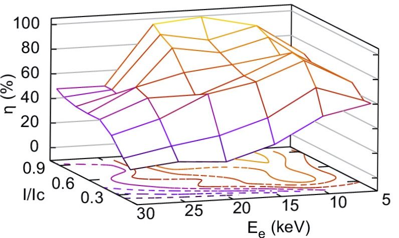
Nanomaterials 2020, 10, 1198                                                                           2 of 20

schemes is presented. Detection of multi-photon signals and photon counting in strong magnetic fields is
discussed in Section 3. Section 4 will then focus on detection of signals from massive particles, beginning
with keV-range energy ions and electrons, then MeV charged particles and will conclude with proposals
on detection of neutrons.

2. SNSPD Concept Origins, Operation and Metrics
     The basic principle behind the photo-detection in SNSPDs is excitation of quasi-electrons out
of the superconducting ground state, an effect that has been first observed almost five decades ago
in thin films of lead [20]. As was shown it the lead film experiments, the formation of the normal
resistive state in the material cannot be explained purely by thermal effects. To fully account for the
experimental results, one has to consider the non-equilibrium dynamics of the superconducting excited
state, with hot quasi-particles at higher temperature than the Cooper pairs of the superconducting
ground state. A more thorough analysis of physics of these processes not limited to applications of
detectors can be found in review of Shklovskij [21], while in this work, we restrict ourselves just to a
quick review of the body of work related to detectors.
     One of the first attempts at quantitative description of this phenomenon was using a two-temperature
model [22], which describes the photoresponse of the superconductor hit by a (not necessarily a single
photon) pulse of light. This model assumes that the photoresponse, which is macroscopically equivalent
to change of the kinetic inductance of the film (inversely proportional to Cooper pair density), has time
constant that is dominated by that of the quasi-particle relaxation time [23–25]. The electron temperature Te
and phonon temperature Tp is then described by a pair of linearized coupled heat-balance equations [26,27]:

                                   dTe       ce
                                ce     =−          Te − Tp + P(t),
                                    dt     τe− p
                                                                                                          (1)
                                   dTp    ce               cp
                                cp     =         Te − Tp −      Tp − T0 ,
                                    dt   τe− p              τes

where ce and c p are electron and phonon specific heat, T0 the heatsink (substrate) temperature, τe− p
the average electron-phonon interaction time, P(t) the absorbed radiation power and τes the time of
phonon escape from superconductor to substrate. The solutions to these equations can be further
related to the film resistance as [22]:
                                                                −1
                                                        Te − Tc

                                R( Te ) = Rn 1 + exp −4              ,                                    (2)
                                                          ∆Tc

where Rn is the normal state resistance and ∆Tc the transition width at a given biasing current.
This model predicts characteristic time constants on the order of 20–30 picoseconds, which is agreement
with experiments carried out on, e.g., NbN microbridges [28,29].
      The spatial dependence of this process was originally studied in context of non-ideal quasi-one-
dimensional superconductors by Skocpol, et al. [30], where the concept of a hot-spot, was first introduced
into the topic. Hot-spot is a region of suppressed order parameter in the superconductor that can form
and persist at temperatures lower than the superconducting critical temperature and was studied in
context of cryotrons (bi-stable superconducting switching devices) [31–34]. This concept was further
elaborated by Kadin, et al. [35] who approximated the Equation (1) by a diffusion equation:

                                           ∂T
                                      Cd      = κd∇2 T + α ( T0 − T ) ,                                   (3)
                                           ∂t
where C = ce + c p is the superconductor specific heat, κ total thermal conductivity of the quasi-particles,
α the superconductor-substrate boundary thermal conductance and Te = Tp = T is the temperature of
the superconductor. Solution to this equation predict single photon-induced hotspots with sizes on the
order of 10–100 nm, which lead to one of the first proposals of the SNSPD devices [36].
Nanomaterials 2020, 10, 1198                                                                                3 of 20

     These models are enough to qualitatively describe the detection process, which can be divided into
multiple stages, that are roughly sketched in Figure 1: A very thin and narrow nanowire is maintained
well below the superconducting critical temperature TC and is constant-current biased at current
values close to critical currents (Figure 1a). Absorption of a single photon with energy much higher
than the superconducting energy gap h̄ω  2∆ ≈ 2 meV will lead to excitation of two quasi-electrons
with high kinetic energies, and those will begin to inelastically scatter with other quasi-particles in the
system. This forms the initial hot-spot [36–40] (Figure 1b). The approximate time-scales associated with
this process are on the order of 10 ps [22] (dictated by the electron-phonon scattering times). The next
stage of the detection process is the expansion of the hot-spot (Figure 1c). First, the quasi-particles
further multiply due to inelastic scattering and move diffusively outwards [41], towards the edges
of the nanowire. The depletion of Cooper pairs leads to local reduction of the order parameter and
redistribution of the current in the region [36]. If the nanowire is biased close to critical currents,
the current density in the hotspot region rises above the critical values and the superconducting state
vanishes completely creating a normal state region that bisects the superconducting wire (Figure 1d).

                                        (d)                       (c)

                                (e)                                       (b)

                                                     (a)
      Figure 1. Schematic of the detection process through the hot spot formation after a photon absorption.
      Equilibrium superconductor is in white, orange to red depicts regions with increasingly suppressed
      order parameter and black lines depict the superconducting current density. Yellow arrow is a schematic
      depiction of an incoming single photon.

      More recent experiments [42] and calculations [43–46] show that this process is also aided by
Abrikosov vortices—While the potential barrier for a vortex entry might be too high in the equilibrium
state, reduction of the order parameter also reduces the nucleation energy and individual vortices might
enter from the wire edges, or vortex-anti-vortex pairs can form and separate. These vortices move across
the wire width due to Lorentz force caused by the flowing current and cause voltage transients, further
reduce the order parameter or cause phase slips [47–51] that can contribute to the device dark counts.
As the section of the wire turns normal, a voltage drop is generated across the wire and this voltage
spike is registered as a resistance spike which corresponds to a single photon detection event. In the
last stage, the current bias is reduced, either passively through a parallel resistive shunt, or actively
using electronically controlled current source and the hot spot shrinks and vanishes, preparing the
nanowire for the next detection event (Figure 1e). The time constant associated with this last step could,
in principle, be determined by how fast the electronic system can cool down to substrate temperature
through interaction with the phonon subsystem—this would be then on the order of the phonon escape
Nanomaterials 2020, 10, 1198                                                                          4 of 20

time τes , which can have values from roughly τe− p to a few nanoseconds [22]. However, in reality this is
primarily determined by the inductance of the device. Many superconductors used in SNSPD devices
have sheet kinetic inductances as high as ∼50 pH/ [52], so a typical ∼100 µm2 area device can have
kinetic inductance around 0.5 µH that leads to the observed time scales of the reset time on the order
of 10 ns.
      While the time from photon absorption to registration of a voltage pulse is approximately 10 ps,
the important metric is the timing jitter, which is the statistical variation of this time delay (typically
reported as FWHM of the distribution). The variation has two contributions: an extrinsic variation due
to geometry of the wire, where there’s a different time delay depending on where along the length of
the wire does the photon get absorbed (in a typical meander geometry, the wire length can reach a
few mm) and jitter associated with the timing of the readout electronics [2]. Then there is the intrinsic
variation that’s due to the probabilistic nature of the processes that lead to the detection event. Typical
values of timing jitter of SNSPD detectors are around 15 ps and are dominated by the noise jitter of
the readout [53], which can reduced down to 7 ps, a value due to geometric jitter [54]. On a short
nano-bridge geometry, the intrinsic timing jitter of 2.7 ps [55] is reported, which is thought as the
current fundamental limit to timing of the SNSPD devices.
      As many of the applications proposed in this work will demand larger pixel sizes than ∼100 µm2 ,
it might be worth elaborating on the current trends on this front: While not as common, detectors
with pixel sizes of the order of 10,000 µm2 are being fabricated [56,57]. Alternatively, one can connect
multiple small SNSPD pixel in parallel to create a large-area “superpixel” [58–62]. An additional
benefit of constructing a detector pixel in this configuration is a better detection rate, because the total
inductance of the superpixel is the harmonic mean of inductances of individual detectors. The tradeoff
is in reduction of SNR of the detector (the voltage drop in inversely proportional to the number of pixels
connected in parallel), but typical signals are on the order of a few mV, so this is not a fundamental
problem unless the number of parallel pixels becomes too large. Lastly, the engineering problems
associated with many-pixel readout are being focused on by many groups working on superconducting
electronics and working arrays of as many as 64 pixels have existed for some time [63–66] and ,coupled
with various switching readout and multiplexing techniques [65,67–72], a kilopixel SNSPD array has
been recently developed [73]. Specifically in the context of particle detection, the covered area can be
further increased by increasing the dimensions wire itself—while this is generally not possible with
photons, charged particles can create hotspots an order of magnitude larger (as will be discussed in
Section 4). This would put nanowire-based particle detector (super)pixels comfortably in the mm-scale
and make them competitive with conventional technologies also in this aspect.
      While most of the previous exposition was not specific to any particular superconducting material, it
might be worth closing the introductory section with a short discussion about materials commonly used
in fabrication of the detectors. The first reported SNSPD was fabricated out of NbN [1], which is still a
popular material to use because of ease of fabrication and comparatively high TC and robustness against
chemical damage during fabrication or operation. Another commonly used materials from the family
of nitrides are TaN [74,75] and NbTiN [52,76,77]. All three of these materials have similar properties in
context of photon detection and decision is usually based on practical factors: Materials with smaller
superconducting gap will have higher relative sensitivity to long wavelength photons. The tradeoff
for better sensitivity in infra-red is lower critical current density and TC , which translates into worse
signal-to-noise ratio and need for better cryogenics. The main drawbacks of this family of materials is
their sensitivity to chemical and physical conditions during thin film deposition, where substantial
efforts have been made to achieve better consistency and process compatibility [78–80], and high
reflectivity [81–83] that makes anti-reflective coatings or integration into photonic cavities necessary
to achieve high quantum efficiency [4,84]. The second common class of SNSPD materials is that of
amorphous superconductors, mostly popular for long wavelength photon detection. The amorphous
nature of the materials allows for fabrication of extremely narrow and thin nanowires and they
generally have smaller superconducting gaps than nitrides, which greatly enhances their IR sensitivity,
Nanomaterials 2020, 10, 1198 5 of 20
as demonstrated with WSi [3], MoSi [85] or MoGe [86], with MoSi also having demonstrated good
performance in UV [87]. The decision between the various amorphous materials is based on the
balance of sensitivity, noise, temperature and jitter, as with the crystalline materials.
An interesting alternative to conventionally used materials are the high-TC superconductors
(specifically cuprates), where alternative detection models are also proposed [88]. The obvious benefits
of using this material the high critical temperature and upper critical magnetic field. The tradeoff in
this case comes mostly from the side of technology, where growth of high-quality superconducting
oxides is a complicated process. YBCO films, which are commonly proposed for high-TC SNSPDs,
require highly specific substrates and growth at excessive temperatures [89–92] and have to be capped
by a passivation layer to prevent degradation [89]. This limits application in detectors that need
on-chip integration with other devices, but one should not discredit their use in detector concepts that
do not require such degree of integration. The highest TC material has been demonstrated in use for
SNSPDs is MgB2 [93,94], however, the material suffers from high sensitivity to oxygen and epitaxy [95],
and single-photon detection has been observed only at temperatures lower than 20 K [96].
When deciding between the whole range of materials, it is important to consider the demands
of the experiment. Nitrides have higher critical temperatures, which allows them operate even at
liquid helium temperatures and they have smaller timing jitter [54,55] but they have lower sensitivity
to long wavelength photons and are limited to smaller number of possible substrates. In context of
NP and HEP experiments, there is also the additional consideration of effects of the environment.
High magnetic fields will favor the polycrystalline materials with high vortex pinning, and devices
made out of these materials currently perform better in these conditions [19,97]. Another option for
magnetic field-tolerant devices would also be to fabricate them out of high-TC materials. Experiments
expecting high radiation fields or high-energy particle bombardment should also tend towards use of
the crystalline materials, specifically NbN, because Nb has comparatively low neutron capture [98]
and scattering [98,99] cross-sections and the short screening length [100,101] makes it more robust
against lattice defects.
3. Non-Standard Photo-Detection Techniques
3.1. Multi-Photon Detection and Multi-Layer Broadband SNSPDs
Most of the applications of SNSPDs are in single photon counting of faint signals in narrow
spectral range and are discussed thoroughly in literature [10,102]. In this review, we want to highlight
techniques that use these devices in different scenarios or configurations, and we start with the less
known applications that still focus on detection of light, which is still of importance to NP and HEP
experiments (e.g., detection of broadband light from Cherenkov radiation, scintillation or ionization)
First such application is number-resolved detection of multi-photon signals, which is commonly
facilitated by visible light photon counters [103,104], transition edge sensors [105], or even Si avalanche
photodiodes [106]. The benefit of using SNSPDs over the other technologies is the superior timing
jitter and rate characteristics and simple readout scheme, while not suffering from the drawbacks of
being confined to narrow temperature regions around room temperature or in the mK range. Typically,
multi-photon resolution is achieved by having arrays of multiple SNSPDs connected in parallel and
use a readout that sums inputs from this array, as demonstrated, e.g., in work of Mattioli, et al. [107].
However, one doesn’t need to limit themselves to SNSPD arrays to achieve multi-photon resolution,
as individual SNSPD devices also have this capability in certain circumstances. These detection
capabilities have been demonstrated by Cahal, et al. [108] in 2017 on standard meander devices made
out of amorphous superconductors. Phenomenological models describing the electro-thermal feedback
during the hot-spot formation [109,110] show that the voltage pulse signal due to multiple nearly
simultaneous detection events (formation of multiple hot-spots within the time-span of nucleation and
expansion stages of the detection process) has a rise time that is inversely proportional to the square
root of total number of hot-spots. Using a simple inductor-resistor differentiating circuit, Cahal, et al.Nanomaterials 2020, 10, 1198 6 of 20
were able to demonstrate photon number resolution at 1550 nm wavelength using approximately 80 ps
attenuated laser pulses, as shown in Figure 2.
Figure 2. Histograms of the peak height of differentiated detection waveforms corresponding to detection
of n-photon signal. The two curves correspond to light wave packets with different mean detected photon
number µ. The arrows with corresponding error bars show predicted values of the peaks from the
electro-thermal model and finite-bandwidth amplifiers. Figure reproduced from Cahal, et al., Optica 4,
1534–1535 (2017) [108].
Another technique, which is not yet standard in SNSPD applications, and could find another
uses in the future is using multi-layer devices, with patterned superconducting layers separated by
dielectric spacing layers [111–114] as shown in Figure 3. As the most popular superconductors used for
SNSPD fabrication have reflectivity of more than 0.5 in most of the interesting wavelength range [115],
one requires to integrate them into photonic cavities or integrate anti-reflective coatings, which turn
them into inherently narrowband detectors. This can be alleviated by tuning the thickness of the dielectric
spacing layers to increase absorption for different wavelengths in different superconducting layers
and effectively making a broadband detector device, as was successfully demonstrated in NbN-based
detectors [111,113]. Similar attempts were made using amorphous WSi as the superconducting
material [112], but they didn’t achieve increase of detection efficiency as with the crystalline materials—
something that is argued in the work to be due to fabrication defects and insufficiently low reduced
working temperature T/TC .
(a) (b)
Figure 3. (a) A two SNSPD-layer device with optical image (left) of the whole structure and a schematic
cross-sectional view in top-right and a SEM image of the SNSPD itself (bottom-right). Figure reproduced
from Verma, et al., Appl. Phys. Lett. 108, 131108 (2016) [114]. (b) Schematic of representation of a
three SNSPD-layer device. Figure reproduced from Florya, et al., Low Temperature Physics 44, 221–225
(2018) [112].Nanomaterials 2020, 10, 1198 7 of 20
3.2. Detection in Strong Magnetic Fields
Before we move on to detection of particles, we should discuss the detection capabilities of
SNSPDs in strong magnetic fields. There exist experiments which require high-rate and high-speed
detection of photons that cannot be covered by conventional technologies.
One example from nuclear physics is the active polarized proton target [116] where an experiment
measure the proton spin-polarizabilities through Compton scattering off a polarized proton target. The
proton spin polarization is achieved via the dynamic nuclear polarization technique of a solid target
held at cryogenic temperatures and in fields as high as 6 T. Within the solid target material the presence
of nuclei, other than the polarized protons, causes a significant background, which can be eliminated by
detecting the recoil proton within the target material. At the required cryogenic temperatures, charge
carrier freeze-out depletes Si-based photomultipliers and causes serious performance degradation [117],
often requiring a complicated optical photon collection scheme and scintillator doping of the target
material [118].
Also, the presence of strong magnetic fields also leads to decrease of detection efficiency, especially
when using photomultiplier tubes. The inefficiency is mitigated by placing the photodetectors
outside of the cryogenic and high-field environment, either by increasing the physical distance [119],
by including magnetic shielding [120], and by guiding the light towards the detector with optical
waveguides or systems of mirrors. Doing this puts a strain on the material budget, induces insertion
losses or attenuation in the medium, and increases timing uncertainty due to dispersion. Considerable
R&D efforts are spent to achieve photon detection performance in at least 1 T [121].
Having detectors in close proximity of the active volume of the experiment, in many cases, would
alleviate these problems. As SNSPDs are superconducting, operation in cryogenic environments
doesn’t cause any degradation in their performance, the only open question was their performance in
magnetic fields. Low-dimensional superconductors (such as superconducting nanowires) can persist
in a Meissner state at fields higher than those for bulk superconductors [122,123], but large transport
currents and the reduction of order parameter during the detection events will lead to reduction of the
Abrikosov vortex nucleation energy barrier [124,125]. These vortices, whether they entered from the
sample surface or formed by unbinding of vortex/anti-vortex pairs (the basic topological excitation
in the 2D superconductors) will move across the sample under action of the Lorentz force from the
transport current and dissipate heat on the order of ∼100 meV per vortex crossing [125,126]. This
can lead to excess dark counts in magnetic fields but also enhance detection of photons that would
be too low-energy to trigger a detection event in a vortex-free superconductor [46,127]. Because of
this direct impact of magnetic fields on the detection mechanism of SNSPDs, considerable work has
been done on studying the effects of small fields, usually not more than 200 mT [128–130], which
is not enough to meet the demands of many potential experiments. However, efforts in geometry
optimization of SNSPD pixels [97,131] and progress in superconductor film deposition technology [78]
allows SNSPDs to operate in fields as high as 0.5 T when applied perpendicular to pixel plane and 5 T
for fields parallel to the pixels [19]. If needed, this values could be potentially increased, if geometry
and material optimization were to be combined [131].
4. Particle Detection
Detection of energetic charged particles can be facilitated by two mechanisms, both of them
sharing the underlying physics of energy loss through interaction with the electron gas or lattice
of the detector material. These interactions are theoretically described by theory of Bethe [132], it’s
modifications by Barkas [133] and Bloch [134] or theory of Firsov [135]. While parameterizations that
use analytical formulas for scattering cross sections exist [136,137] and could be used to determine
energy loss approximately, it is more common to employ numerical methods for this purpose.Nanomaterials 2020, 10, 1198 8 of 20
The first mechanism is scattering on the superconducting electrons directly, or indirectly through
lattice phonons. The effect is no different from the photon absorption process described in Section 2—
if the scattered particle deposits enough energy to break apart a Cooper pair, the excited quasi-particles
will behave the same as those excited by photons.
The second mechanism is a thermal process, first proposed for detector purposes by Scherman [138].
In this thermal process, the hotspot in the nanowire is not created by diffusion and multiplication of
quasi-particles, but by direct heat exchange with the microplasma in the particle track. In these tracks,
the radius of a (locally) cylindrical region at temperature at least Tm is approximately [138–140]
s
Q
rhs ≈ , (4)
eπcρ ( Tm − T0 )
where Q is the energy loss per unit length (assumed here to stay constant through the thin film), c the
superconductor specific heat, ρ the density and T0 is the temperature of the substrate. By setting the
temperature Tm equal to superconducting critical temperature Tc and carrying out a Monte-Carlo
simulation [141] for values of Q, we can determine that the thermal hotspot radius in NbN detectors is
of the order of 50–100 nm (see Figure 4). This number is only for the thermal hotspot “core”, where
superconductivity is suppressed completely. Area of the region with suppressed order parameter and
increased thermal fluctuations is larger than that, as the temperature increase is ∆T ∝ r12 .
110 NbN
W0.76 Si0.24
100
90
rhs [nm]
80
70
60
50
40
104 105 106 107
Eα [eV]
Figure 4. Approximate thermal hotspot radius rhs as a function of α-particle kinetic energy in NbN
film with TC = 8K and W0.76 Si0.24 film with TC = 3.35 K. Both films are assumed to be held at T0 = T2C .
This result demonstrates that SNSPDs should work not only as high efficiency single photon
detectors, but also as detectors of single charged particles. There are, however, differences: In the
few eV energy ranges of photonics experiments, the size of the hotspot is a monotonously increasing
function of the photon energy [36,142]. With high energy particles, this is not necessarily true and one
has to expect a rolloff at high energies, because the stopping power S (the retarding force that slows
the particles in physical media) begins decreasing [143]. Because of this, Q (that is effectively equal
to work done by stopping power S) is mostly independent on the particle energy only for E . 1 keV,
after which there is a non-monotonic dependence on energy, as can be seen in Figure 4. can have on the
detection process of particles: In case of photons, the detection process relies on scattering of a photon
into a highly energetic quasi-electron pair in the volume of the superconductor. With charged particles,
there is the possibility that they penetrate through the SNSPD material with minimal energy loss and
interact deeper in the substrate, causing knockoff reactions or they can emit a large amount of photons
and phonons as they stop due to rapid scattering at the Bragg peak—these can be energetic enough toNanomaterials 2020, 10, 1198 9 of 20
still trigger a detection event, but the probability also has a high-energy rolloff as the particle range
increases with energy and the Bragg peak moves deeper into the substrate [144].
4.1. Low Energy Ion Detection
The concept of detecting low energy molecules has already found a limited use in high-performance
time-of-flight mass spectrometry [145], particularly in the form of micron-sized superconducting
stripline detectors [146–149], which demonstrate that parallel superconducting wires provide both,
high mass resolution and limited charge state discrimination of ions [150] or lysozyme molecules—this
technology is discussed in greater detail in a review by Cristiano, et al. [151]. It is also worth mentioning
that it is here, where MgB2 -based devices found applications as biomolecular detectors [152].
On the other hand, the idea of using . 100 nm wide SNSPDs for light particle detection purposes
is a relatively unexplored concept. Several successful attempts have already been made in detecting
positive ions. The first is by Sclafani, et al. [153], where it has been demonstrated that SNSPDs are
capable of detection of He+ ions with energies up to 1 keV with 100% detection efficiency, as shown in
the device bias sweeps in Figure 5a. One of the important takeaways of their analysis, based on that of
Verevkin et al. [142], is that the initial hot-spot caused by a He+ ion is 10–20 times bigger than that of a
photon with equivalent energy, which would support the model of thermal hotspots discussed in the
previous paragraphs.
Another important result is that surface adsorbates, which are usually ignored in the context of
photon detection, start to play an important role in detection of low energy ions, where the detection
efficiency can drop by more than three orders of magnitude as the density of surface contaminants
increases, as seen in Figure 5b. This is an important consideration for application in mass spectrometry,
however, it might become unimportant for detection of high energy particles in NP and HEP applications,
where the penetration depth of MeV and higher energy particles is easily more than 10 µm [144].
(a) (b)
Figure 5. (a) Demonstration of capability of 100% detection efficiency of He+ particles with kinetic
energies of 200 eV (square), 400 eV (circle), 600 eV (up-triangle), 800 eV (down-triangle) and 1000 eV
(diamond). The points Ikb corresponds to bias current value where the primary cause for hot-spot
expansion changes from fluctuation-based into current-crowding regime. (b) Relative detection
efficiency as a function of accumulated deposition time of neutral He atoms. Figures reproduced
from Sclafani, et al., Nanotechnology 23, 065501 (2012) [153].
4.2. Low Energy Electron Detection
Following in the vein of detection of particles in the keV-range, another important results were
shown by Rosticher, et al. [154], who achieve nearly 100% detection efficiency for electrons with kinetic
energies up to 20 keV. In their work, Rosticher, et al. show that a SNSPD device is capable of detecting
an incoming electron even if the collision doesn’t happen in the superconducting film (Figure 6a).
This supports the notion that the detection does not happen just in the superconducting nanowire,Nanomaterials 2020, 10, 1198 10 of 20
but that the substrate plays an active role in the process, which explains why the detection efficiencies
in particle detection can reach 100% even though the active area covered by the superconducting
meander is only ≈50% and has been confirmed by the authors through a Monte-Carlo simulation of
the electron kinematics. Further, these results demonstrate the previously discussed importance of
stopping power of the superconducting material and the substrate, as can be clearly seen in the loss
of detection efficiency at high electron kinetic energies in Figure 6b: The energy loss of an electron
in certain materials is approximately inversely proportional to the kinetic energy [155], which means
that it penetrates deeper into the material before meaningful amounts of energy are transferred into
the substrate. If not enough energy is lost while in proximity of the nanowire, any meaningful energy
transfer to the superconducting system cannot happen and the electron will not get detected. This effects
leads to degradation of detection efficiency in bare SNSPD devices, however by adding a stopping layer
on top of the device, one could exploit this effect and design a detector of particles only within a certain
energy range that can be tuned by varying the thickness or density of the additional material.
(a) (b)
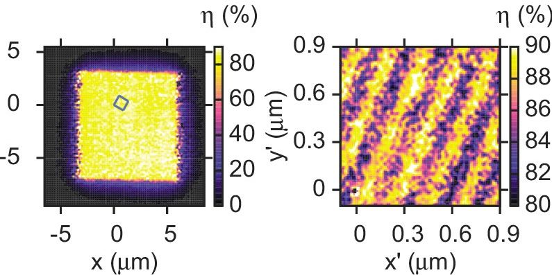
Figure 6. (a) Map of detection efficiency across the SNSPD pixel (left) under bombardment of 20 keV
electrons, with a zoom in on a small part of the meander showing the non-zero detection probability
outside of the superconducting meander. (b) A parameter sweep map that show the electron detection
efficiency as a function of the reduced device bias current I/IC and electron kinetic energy Ee . Figures
reproduced from Rosticher, et al., Appl. Phys. Lett. 97, 183106 (2010) [154].
4.3. High Energy Particle Detection
In the scope of NP and HEP experiments, it is important to determine if SNSPDs are capable of
detection of particles not in the few keV energy range, but particles with kinetic energies from a few
MeV and up to relativistic cases, where energies will go as high as few GeV. Detection of relativistic
particles with SNSPDs has not been studied in literature, but the lower end of the range was explored
by Azzouz, et al. [156], who demonstrated detection of MeV α and β− particles from 210 Po and 42 K
or 31 Si sources, respectively. The detection efficiency was lowest for the 5 MeV α-particles, reported
to be 78 ± 18% and over the timespan of 4 days, Azzouz, et al. have not seen any degradation in
noise, timing or efficiency, demonstrating good radiation hardness of NbTiN SNSPDs in this radiation
environment. By using an 241 Am source covered by thin aluminum foil, Azzouz, et al. were also able to
show that their devices are insensitive to nominally 5.95 keV γ and X-ray photons (efficiency reported
as 0 ± 10%). This is an interesting result, especially in context of the previously mentioned comparison
of effects of ions and photons of equivalent energies by Sclafani, et al., that deserves future study.
It also has immediate positive implications on certain experiments. For example in cases of nuclear
recoil and photodisintegration measurements, one uses high-energy photons [157,158] to drive this
process but, for the detectors, this γ-ray beam is a considerable source of noise, especially if scattered.
Having sensitivity only to lower energy photons or charged particles would greatly benefit statistics of
these experiments.Nanomaterials 2020, 10, 1198 11 of 20
4.4. Neutron and Dark Matter Detection
Detection of charged particles is relatively straightforward because of comparatively high scattering
cross sections with the lattice and electrons of the superconductor and substrate. There might be,
however, desire to use SNSPDs to detect neutral or weakly interacting particles such as neutrons or
potential dark matter candidates. Working detection schemes utilizing SNSPDs are not yet developed
but, for detection of neutrons, there exists a related technology that was used to demonstrate this
capability: current biased kinetic inductance detectors (CBKID) [159–161]. The operation of CBKIDs
is slightly different from SNSPDs, where one detects changes of kinetic inductance due to partial
suppression of superconductivity in a large meandering superconducting stripline instead of change of
DC resistance of a nanoscale meander, but the main operation principle can be transferred between the
two technologies. In the works of Iizawa et al. [160] and Shishido et al. [161], a separate layer of 10 B,
while in work of Yoshioka, et al. [162] a more direct approach was used when detectors were fabricated
out of superconducting MgB2 . 10 B in the devices converts neutrons into energetic 4 He and 7 Li ions
detected using a differential readout of the CBKID delay line, which allowed for a spatially-resolved
measurement of neutron flux. Because the main neutron detection mechanism is through the conversion
into charged particles, one can, in principle, substitute the CBKID devices with SNSPDs and construct
a high-rate and high-speed detector of neutron flux with the same characteristics as discussed in the
previous sections.
The last application mentioned here is in detection of dark matter. As attempts to detect dark
matter with mass above the GeV scale are so far fruitless, researchers are coming up with proposals
of detection of MeV-scale dark matter in semiconductors [163,164], or even lower energies, where
superconductors can be used for direct detection through dark matter-electron scattering [165,166]. As of
the time of writing of this review, there is no concrete realization SNSPD dark matter search experiment,
but Hochberg et al. propose use of NbN-based SNSPDs as target and sensor for ultra-light dark
matter [167], citing high sensitivity and very low dark counts when compared to existing experiments.
5. Conclusions
Many experiments in nuclear, high energy and astrophysics have demands that can be uniquely
met by the capabilities of superconducting nanowire detectors. We discussed applications of SNSPDs
that go beyond just detection of low-energy photons in low-background environments and show
that there exist demonstrations of the technology being robust enough for development of detectors
based on SNSPDs, especially in small to medium-scale experiments. Further work needs to be
done, especially on the front of systematic characterization of performance of high energy particle
detection and integration into large-scale experiments, however, this effort represents opportunity for
experiments that are currently near impossible with conventional technologies.
Author Contributions: Writing—original draft, T.P.; Investigaton, T.P. and W.A.; Writing—review & editing, W.A.,
G.K., Z.-E.M. and V.N.; Visualization, T.P.; Project administration, Z.-E.M.; Supervision, G.K. and V.N. All authors
have read and agreed to the published version of the manuscript.
Funding: This work was supported by the U. S. Department of Energy (DOE), Office of Science, Offices of Nuclear
Physics, Basic Energy Sciences, Materials Sciences and Engineering Division under Contract # DE-AC02-06CH11357.
Conflicts of Interest: The authors declare no conflict of interest.
References
1. Gol’Tsman, G.; Okunev, O.; Chulkova, G.; Lipatov, A.; Semenov, A.; Smirnov, K.; Voronov, B.; Dzardanov, A.;
Williams, C.; Sobolewski, R. Picosecond superconducting single-photon optical detector. Appl. Phys. Lett.
2001, 79, 705–707. [CrossRef]
2. Wu, J.; You, L.; Chen, S.; Li, H.; He, Y.; Lv, C.; Wang, Z.; Xie, X. Improving the timing jitter of a
superconducting nanowire single-photon detection system. Appl. Opt. 2017, 56, 2195–2200. [CrossRef]
[PubMed]Nanomaterials 2020, 10, 1198 12 of 20
3. Marsili, F.; Verma, V.B.; Stern, J.A.; Harrington, S.; Lita, A.E.; Gerrits, T.; Vayshenker, I.; Baek, B.; Shaw, M.D.;
Mirin, R.P.; et al. Detecting single infrared photons with 93% system efficiency. Nat. Photonics 2013, 7, 210.
[CrossRef]
4. Zhang, W.; You, L.; Li, H.; Huang, J.; Lv, C.; Zhang, L.; Liu, X.; Wu, J.; Wang, Z.; Xie, X. NbN superconducting
nanowire single photon detector with efficiency over 90% at 1550 nm wavelength operational at compact
cryocooler temperature. Sci. China Phys. Mech. Astron. 2017, 60, 120314. [CrossRef]
5. Shibata, H.; Shimizu, K.; Takesue, H.; Tokura, Y. Ultimate low system dark-count rate for superconducting
nanowire single-photon detector. Opt. Lett. 2015, 40, 3428–3431. [CrossRef]
6. Zhu, J.; Chen, Y.; Zhang, L.; Jia, X.; Feng, Z.; Wu, G.; Yan, X.; Zhai, J.; Wu, Y.; Chen, Q.; et al. Demonstration
of measuring sea fog with an SNSPD-based Lidar system. Sci. Rep. 2017, 7, 1–7. [CrossRef]
7. Takesue, H.; Dyer, S.D.; Stevens, M.J.; Verma, V.; Mirin, R.P.; Nam, S.W. Quantum teleportation over 100 km
of fiber using highly efficient superconducting nanowire single-photon detectors. Optica 2015, 2, 832–835.
[CrossRef]
8. Takesue, H.; Nam, S.W.; Zhang, Q.; Hadfield, R.H.; Honjo, T.; Tamaki, K.; Yamamoto, Y. Quantum key
distribution over a 40-dB channel loss using superconducting single-photon detectors. Nat. Photonics 2007,
1, 343. [CrossRef]
9. Chen, J.; Altepeter, J.B.; Medic, M.; Lee, K.F.; Gokden, B.; Hadfield, R.H.; Nam, S.W.; Kumar, P.
Demonstration of a quantum controlled-NOT gate in the telecommunications band. Phys. Rev. Lett. 2008,
100, 133603. [CrossRef]
10. Natarajan, C.M.; Tanner, M.G.; Hadfield, R.H. Superconducting nanowire single-photon detectors: Physics
and applications. Supercond. Sci. Technol. 2012, 25, 063001. [CrossRef]
11. Hewett, J.; Weerts, H.; Brock, R.; Butler, J.; Casey, B.; Collar, J.; de Gouvea, A.; Essig, R.; Grossman, Y.;
Haxton, W.; et al. Fundamental physics at the intensity frontier. arXiv 2012, arXiv:1205.2671.
12. Bull, P.; Fitzgerald, J.; Harris, R.; Gunarathne, D.; Kaczanowics, E.; Kraishan, A.; Li, X.; McCormick, M.;
Meziani, Z.; Miller, G.; et al. Design and Assembly of Fast and Lightweight Barrel and Forward Tracking
Prototype Systems for an EIC. Available online: https://wiki.bnl.gov/conferences/images/7/78/EIC-
RD2013-3-Status-Proposal-Saclay-TU.pdf (accessed on 18 May 2020).
13. Niinikoski, T.; Abreu, M.; Anbinderis, P.; Anbinderis, T.; D’Ambrosio, N.; De Boer, W.; Borchi, E.; Borer, K.;
Bruzzi, M.; Buontempo, S.; et al. Low-temperature tracking detectors. Nuclear Instrum. Methods Phys. Res.
Sect. A Accel. Spectrom. Detect. Assoc. Equip. 2004, 520, 87–92. [CrossRef]
14. Abelev, B.; Adam, J.; Adamová, D.; Aggarwal, M.; Rinella, G.A.; Agnello, M.; Agostinelli, A.; Agrawal, N.;
Ahammed, Z.; Ahmad, N.; et al. Technical design report for the upgrade of the ALICE inner tracking system.
J. Phys. G Nucl. Part. Phys. 2014, 41, 087002. [CrossRef]
15. Adare, A.; Aidala, C.; Ajitanand, N.; Akiba, Y.; Akimoto, R.; Alfred, M.; Apadula, N.; Aramaki, Y.; Asano, H.;
Atomssa, E.; et al. Concept for an Electron Ion Collider (EIC) detector built around the BaBar solenoid. arXiv
2014, arXiv:1402.1209.
16. Khalek, S.A.; Allongue, B.; Anghinolfi, F.; Barrillon, P.; Blanchot, G.; Blin-Bondil, S.; Braem, A.; Chytka, L.;
Muino, P.C.; Düren, M.; et al. The ALFA roman pot detectors of ATLAS. J. Instrum. 2016, 11, P11013.
[CrossRef]
17. Bültmann, S.; Chen, W.; Chiang, I.; Chrien, R.; Drees, A.; Gill, R.; Guryn, W.; Landgraf, J.; Li, Z.; Ljubicic, T.;
et al. The PP2PP experiment at RHIC: Silicon detectors installed in Roman Pots for forward proton detection
close to the beam. Nucl. Instrum. Methods Phys. Res. Sect. A Accel. Spectrom. Detect. Assoc. Equip. 2004,
535, 415–420. [CrossRef]
18. Ruggiero, G.; Avati, V.; Antchev, G.; Deile, M.; Eggert, K.; Eremin, V.; Kaspar, J.; Niewiadomski, H.;
Petäjäjärvi, J.; Radicioni, E.; et al. Characteristics of edgeless silicon detectors for the Roman Pots of the
TOTEM experiment at the LHC. Nucl. Instrum. Methods Phys. Res. Sect. A Accel. Spectrom. Detect. Assoc. Equip.
2009, 604, 242–245. [CrossRef]
19. Polakovic, T.; Armstrong, W.; Yefremenko, V.; Pearson, J.; Hafidi, K.; Karapetrov, G.; Meziani, Z.E.;
Novosad, V. Superconducting nanowires as high-rate photon detectors in strong magnetic fields. Nucl.
Instrum. Methods Phys. Res. Sect. A Accel. Spectrom. Detect. Assoc. Equip. 2020, 959, 163543. [CrossRef]Nanomaterials 2020, 10, 1198 13 of 20
20. Testardi, L. Destruction of superconductivity by laser light. Phys. Rev. B 1971, 4, 2189. [CrossRef]
21. Shklovskij, V. Hot electrons in metal films at low temperatures. Low Temp. Phys. 2018, 44, 165–183. [CrossRef]
22. Semenov, A.; Nebosis, R.; Gousev, Y.P.; Heusinger, M.; Renk, K. Analysis of the nonequilibrium
photoresponse of superconducting films to pulsed radiation by use of a two-temperature model. Phys. Rev. B
1995, 52, 581. [CrossRef] [PubMed]
23. Gershenzon, E.; Gol’tsman, G.; Semenov, A.; Sergeev, A. Mechanism of picosecond response of granular
YBaCuO films to electromagnetic radiation. Solid State Commun. 1990, 76, 493–497. [CrossRef]
24. Sergeev, A. Nonselective effect of electromagnetic radiation on a superconducting film in the resistive state.
JETP Lett. 1982, 36, 244.
25. Maneval, J.P.; Chibane, F.; Bland, R. Electron-phonon decoupling in the photoresponse of YBaCuO granular
films at low temperature. Appl. Phys. Lett. 1992, 61, 339–341. [CrossRef]
26. Perrin, N.; Vanneste, C. Response of superconducting films to a periodic optical irradiation. Phys. Rev. B
1983, 28, 5150. [CrossRef]
27. Frenkel, A. Mechanism of nonequilibrium optical response of high-temperature superconductors.
Phys. Rev. B 1993, 48, 9717. [CrossRef]
28. Gol’Tsman, G.; Semenov, A.; Gousev, Y.P.; Zorin, M.; Godidze, I.; Gershenzon, E.; Lang, P.; Knott, W.;
Renk, K. Sensitive picosecond NbN detector for radiation from millimetre wavelengths to visible light.
Supercond. Sci. Technol. 1991, 4, 453. [CrossRef]
29. Lindgren, M.; Currie, M.; Zeng, W.S.; Sobolewski, R.; Cherednichenko, S.; Voronov, B.; Gol’tsman, G.
Picosecond response of a superconducting hot-electron NbN photodetector. Appl. Supercond. 1998, 6, 423–428.
[CrossRef]
30. Skocpol, W.; Beasley, M.; Tinkham, M. Self-heating hotspots in superconducting thin-film microbridges.
J. Appl. Phys. 1974, 45, 4054–4066. [CrossRef]
31. Bremer, J.W.; Newhouse, V. Thermal propagation effect in thin superconducting films. Phys. Rev. Lett. 1958,
1, 282. [CrossRef]
32. Broom, R.; Rhoderick, E. A New Type of Bistable Element Involving Thermal Propagation of a Normal Region
in a Thin Superconducting Film; Office of Naval Research, Department of the Navy: Arlington, VA, USA,
1960; p. 113.
33. Broom, R.; Rhoderick, E. Thermal propagation of a normal region in a thin superconducting film and its
application to a new type of bistable element. Br. J. Appl. Phys. 1960, 11, 292. [CrossRef]
34. Cherry, W.; Gittleman, J. Thermal and electrodynamic aspects of the superconductive transition process.
Solid-State Electron. 1960, 1, 287–305. [CrossRef]
35. Kadin, A.; Johnson, M. Nonequilibrium photon-induced hotspot: A new mechanism for photodetection in
ultrathin metallic films. Appl. Phys. Lett. 1996, 69, 3938–3940. [CrossRef]
36. Semenov, A.D.; Gol’tsman, G.N.; Korneev, A.A. Quantum detection by current carrying superconducting
film. Phys. C Supercond. 2001, 351, 349–356. [CrossRef]
37. Il’in, K.; Lindgren, M.; Currie, M.; Semenov, A.; Gol’Tsman, G.; Sobolewski, R.; Cherednichenko, S.;
Gershenzon, E. Picosecond hot-electron energy relaxation in NbN superconducting photodetectors.
Appl. Phys. Lett. 2000, 76, 2752–2754. [CrossRef]
38. Vodolazov, D.Y. Single-photon detection by a dirty current-carrying superconducting strip based on the
kinetic-equation approach. Phys. Rev. Appl. 2017, 7, 034014. [CrossRef]
39. Zotova, A.; Vodolazov, D.Y. Photon detection by current-carrying superconducting film: A time-dependent
Ginzburg-Landau approach. Phys. Rev. B 2012, 85, 024509. [CrossRef]
40. Engel, A.; Schilling, A. Numerical analysis of detection-mechanism models of superconducting nanowire
single-photon detector. J. Appl. Phys. 2013, 114, 214501. [CrossRef]
41. Semenov, A.D.; Gol’tsman, G.N. Nonthermal mixing mechanism in a diffusion-cooled hot-electron detector.
J. Appl. Phys. 2000, 87, 502–510. [CrossRef]
42. Casaburi, A.; Heath, R.; Ejrnaes, M.; Nappi, C.; Cristiano, R.; Hadfield, R. Experimental evidence of
photoinduced vortex crossing in current carrying superconducting strips. Phys. Rev. B 2015, 92, 214512.
[CrossRef]Nanomaterials 2020, 10, 1198 14 of 20
43. Vodolazov, D.Y.; Korneeva, Y.P.; Semenov, A.; Korneev, A.; Goltsman, G. Vortex-assisted mechanism of
photon counting in a superconducting nanowire single-photon detector revealed by external magnetic field.
Phys. Rev. B 2015, 92, 104503. [CrossRef]
44. Zotova, A.; Vodolazov, D.Y. Intrinsic detection efficiency of superconducting nanowire single photon detector
in the modified hot spot model. Supercond. Sci. Technol. 2014, 27, 125001. [CrossRef]
45. Sidorova, M.; Semenov, A.; Hübers, H.W.; Kuzmin, A.; Doerner, S.; Ilin, K.; Siegel, M.; Charaev, I.;
Vodolazov, D. Timing jitter in photon detection by straight superconducting nanowires: Effect of magnetic
field and photon flux. Phys. Rev. B 2018, 98, 134504. [CrossRef]
46. Bulaevskii, L.N.; Graf, M.J.; Kogan, V.G. Vortex-assisted photon counts and their magnetic field dependence
in single-photon superconducting detectors. Phys. Rev. B 2012, 85, 014505. [CrossRef]
47. Bezryadin, A.; Lau, C.; Tinkham, M. Quantum suppression of superconductivity in ultrathin nanowires.
Nature 2000, 404, 971–974. [CrossRef] [PubMed]
48. Andronov, A.; Gordion, I.; Kurin, V.; Nefedov, I.; Shereshevsky, I. Kinematic vortices and phase slip lines in
the dynamics of the resistive state of narrow superconductive thin film channels. Phys. C Supercond. Its Appl.
1993, 213, 193–199. [CrossRef]
49. Michotte, S.; Mátéfi-Tempfli, S.; Piraux, L.; Vodolazov, D.; Peeters, F. Condition for the occurrence of phase
slip centers in superconducting nanowires under applied current or voltage. Phys. Rev. B 2004, 69, 094512.
[CrossRef]
50. Vodolazov, D.Y. Negative magnetoresistance and phase slip process in superconducting nanowires.
Phys. Rev. B 2007, 75, 184517. [CrossRef]
51. Elmurodov, A.; Peeters, F.; Vodolazov, D.; Michotte, S.; Adam, S.; de Horne, F.d.M.; Piraux, L.; Lucot, D.;
Mailly, D. Phase-slip phenomena in NbN superconducting nanowires with leads. Phys. Rev. B 2008,
78, 214519. [CrossRef]
52. Miki, S.; Takeda, M.; Fujiwara, M.; Sasaki, M.; Otomo, A.; Wang, Z. Superconducting NbTiN nanowire single
photon detectors with low kinetic inductance. Appl. Phys. Express 2009, 2, 075002. [CrossRef]
53. Zhao, Q.; Zhang, L.; Jia, T.; Kang, L.; Xu, W.; Chen, J.; Wu, P. Intrinsic timing jitter of superconducting
nanowire single-photon detectors. Appl. Phys. B 2011, 104, 673–678. [CrossRef]
54. Calandri, N.; Zhao, Q.Y.; Zhu, D.; Dane, A.; Berggren, K.K. Superconducting nanowire detector jitter limited
by detector geometry. Appl. Phys. Lett. 2016, 109, 152601. [CrossRef]
55. Korzh, B.; Zhao, Q.Y.; Frasca, S.; Allmaras, J.; Autry, T.; Bersin, E.A.; Colangelo, M.; Crouch, G.; Dane, A.;
Gerrits, T.; et al. Demonstrating sub-3 ps temporal resolution in a superconducting nanowire single-photon
detector. arXiv 2018, arXiv:1804.06839.
56. Lv, C.; Zhou, H.; Li, H.; You, L.; Liu, X.; Wang, Y.; Zhang, W.; Chen, S.; Wang, Z.; Xie, X. Large active area
superconducting single-nanowire photon detector with a 100 µm diameter. Supercond. Sci. Technol. 2017,
30, 115018. [CrossRef]
57. Li, H.; Zhang, L.; You, L.; Yang, X.; Zhang, W.; Liu, X.; Chen, S.; Wang, Z.; Xie, X. Large-sensitive-area
superconducting nanowire single-photon detector at 850 nm with high detection efficiency. Opt. Express
2015, 23, 17301–17308. [CrossRef]
58. Ejrnaes, M.; Cristiano, R.; Quaranta, O.; Pagano, S.; Gaggero, A.; Mattioli, F.; Leoni, R.; Voronov, B.;
Gol’Tsman, G. A cascade switching superconducting single photon detector. Appl. Phys. Lett. 2007,
91, 262509. [CrossRef]
59. Ejrnaes, M.; Casaburi, A.; Quaranta, O.; Marchetti, S.; Gaggero, A.; Mattioli, F.; Leoni, R.; Pagano, S.; Cristiano,
R. Characterization of parallel superconducting nanowire single photon detectors. Supercond. Sci. Technol.
2009, 22, 055006. [CrossRef]
60. Nam, S.; Calkins, B.; Gerritts, T.; Harrington, S.; Lita, A.; Marsili, F.; Verma, V.; Vayshenker, I.; Mirin, R.; Shaw,
M.; et al. Superconducting nanowire avalanche photodetectors. In Proceedings of the 2013 IEEE Photonics
Conference, Bellevue, WA, USA, 8–12 September 2013; IEEE: Piscataway, NJ, USA, 2013; pp. 366–367.
61. Heath, R.M.; Tanner, M.G.; Casaburi, A.; Webster, M.G.; San Emeterio Alvarez, L.; Jiang, W.; Barber, Z.H.;
Warburton, R.J.; Hadfield, R.H. Nano-optical observation of cascade switching in a parallel superconducting
nanowire single photon detector. Appl. Phys. Lett. 2014, 104, 063503. [CrossRef]Nanomaterials 2020, 10, 1198 15 of 20
62. Cheng, R.; Poot, M.; Guo, X.; Fan, L.; Tang, H.X. Large-area superconducting nanowire single-photon
detector with double-stage avalanche structure. IEEE Trans. Appl. Supercond. 2016, 27, 1–5. [CrossRef]
63. Miki, S.; Yamashita, T.; Wang, Z.; Terai, H. A 64-pixel NbTiN superconducting nanowire single-photon
detector array for spatially resolved photon detection. Opt. Express 2014, 22, 7811–7820. [CrossRef]
64. Shaw, M.; Marsili, F.; Beyer, A.; Stern, J.; Resta, G.; Ravindran, P.; Chang, S.; Bardin, J.; Russell, D.; Gin, J.; et al.
Arrays of WSi superconducting nanowire single photon detectors for deep-space optical communications.
In Proceedings of the 2015 Conference on Lasers and Electro-Optics (CLEO), San Jose, CA, USA, 10–15 May
2015; IEEE: Piscataway, NJ, USA, 2015; pp. 1–2.
65. Allman, M.S.; Verma, V.B.; Stevens, M.; Gerrits, T.; Horansky, R.D.; Lita, A.E.; Marsili, F.; Beyer, A.; Shaw, M.;
Kumor, D.; et al. A near-infrared 64-pixel superconducting nanowire single photon detector array with
integrated multiplexed readout. Appl. Phys. Lett. 2015, 106, 192601. [CrossRef]
66. Allmaras, J.; Beyer, A.; Briggs, R.; Marsili, F.; Shaw, M.; Resta, G.; Stern, J.; Verma, V.; Mirin, R.;
Nam, S.; et al. Large-area 64-pixel array of WSi superconducting nanowire single photon detectors. In CLEO:
QELS_Fundamental Science; Optical Society of America: Washington, DC, USA, 2017; pp. JTh3E–7.
67. Engert, S.; Wetzstein, O.; Hofherr, M.; Ilin, K.; Siegel, M.; Meyer, H.G.; Toepfer, H. Mathematical analysis of
multiplexing techniques for SNSPD arrays. IEEE Trans. Appl. Supercond. 2013, 23, 2501005. [CrossRef]
68. Hofherr, M.; Arndt, M.; Il’In, K.; Henrich, D.; Siegel, M.; Toussaint, J.; May, T.; Meyer, H.G. Time-
tagged multiplexing of serially biased superconducting nanowire single-photon detectors. IEEE Trans.
Appl. Supercond. 2013, 23, 2501205. [CrossRef]
69. Miyajima, S.; Yabuno, M.; Miki, S.; Yamashita, T.; Terai, H. High-time-resolved 64-channel single-flux
quantum-based address encoder integrated with a multi-pixel superconducting nanowire single-photon
detector. Opt. Express 2018, 26, 29045–29054. [CrossRef] [PubMed]
70. Gaggero, A.; Martini, F.; Mattioli, F.; Chiarello, F.; Cernansky, R.; Politi, A.; Leoni, R. Amplitude-multiplexed
readout of single photon detectors based on superconducting nanowires. Optica 2019, 6, 823–828. [CrossRef]
71. Sinclair, A.; Schroeder, E.; Zhu, D.; Colangelo, M.; Glasby, J.; Mauskopf, P.; Mani, H.; Berggren, K.
Demonstration of microwave multiplexed readout of DC-biased superconducting nanowire detectors.
IEEE Trans. Appl. Supercond. 2019, 29, 1–4. [CrossRef]
72. Allmaras, J.P.; Wollman, E.E.; Beyer, A.D.; Briggs, R.M.; Korzh, B.A.; Bumble, B.; Shaw, M.D.
Demonstration of a Thermally Coupled Row-Column SNSPD Imaging Array. Nano Lett. 2020, 20, 2163–2168.
[CrossRef]
73. Wollman, E.E.; Verma, V.B.; Lita, A.E.; Farr, W.H.; Shaw, M.D.; Mirin, R.P.; Nam, S.W. Kilopixel array of
superconducting nanowire single-photon detectors. Opt. Express 2019, 27, 35279–35289. [CrossRef]
74. Engel, A.; Aeschbacher, A.; Inderbitzin, K.; Schilling, A.; Il’in, K.; Hofherr, M.; Siegel, M.; Semenov,
A.; Hübers, H.W. Tantalum nitride superconducting single-photon detectors with low cut-off energy.
Appl. Phys. Lett. 2012, 100, 062601. [CrossRef]
75. Il’in, K.; Hofherr, M.; Rall, D.; Siegel, M.; Semenov, A.; Engel, A.; Inderbitzin, K.; Aeschbacher, A.; Schilling, A.
Ultra-thin TaN films for superconducting nanowire single-photon detectors. J. Low Temp. Phys. 2012,
167, 809–814. [CrossRef]
76. Tanner, M.G.; Natarajan, C.; Pottapenjara, V.; O’Connor, J.; Warburton, R.; Hadfield, R.; Baek, B.; Nam, S.;
Dorenbos, S.; Ureña, E.B.; et al. Enhanced telecom wavelength single-photon detection with NbTiN
superconducting nanowires on oxidized silicon. Appl. Phys. Lett. 2010, 96, 221109. [CrossRef]
77. Miki, S.; Yamashita, T.; Terai, H.; Wang, Z. High performance fiber-coupled NbTiN superconducting
nanowire single photon detectors with Gifford-McMahon cryocooler. Opt. Express 2013, 21, 10208–10214.
[CrossRef] [PubMed]
78. Polakovic, T.; Lendinez, S.; Pearson, J.E.; Hoffmann, A.; Yefremenko, V.; Chang, C.L.; Armstrong, W.;
Hafidi, K.; Karapetrov, G.; Novosad, V. Room temperature deposition of superconducting niobium nitride
films by ion beam assisted sputtering. APL Mater. 2018, 6, 076107. [CrossRef]
79. Dane, A.E.; McCaughan, A.N.; Zhu, D.; Zhao, Q.; Kim, C.S.; Calandri, N.; Agarwal, A.; Bellei, F.; Berggren,
K.K. Bias sputtered NbN and superconducting nanowire devices. Appl. Phys. Lett. 2017, 111, 122601.
[CrossRef]You can also read