A bidirectional threshold switching selector with a symmetric multilayer structure
←
→
Page content transcription
If your browser does not render page correctly, please read the page content below
SCIENCE CHINA
                                                Information Sciences
. RESEARCH PAPER .                                                                         April 2021, Vol. 64 142402:1–142402:6
                                                                                       https://doi.org/10.1007/s11432-020-2960-x

     A bidirectional threshold switching selector with
             a symmetric multilayer structure
               Qingjiang LI, Kun LI, Yongzhou WANG, Sen LIU & Bing SONG*
     College of Electronic Science and Technology, National University of Defense Technology, Changsha 410073, China

             Received 3 May 2020/Revised 3 June 2020/Accepted 18 June 2020/Published online 23 November 2020

       Abstract Selectors have been proposed as a highly effective tool for suppressing substantial leakage currents
       without sacrificing the high density of resistive random-access memory (RRAM) crossbar arrays. Among vari-
       ous selector types, the programmable metallization cell (PMC) selector is promising due to its simple structure
       and high selectivity. In this work, we demonstrate a new PMC selector that exhibits bidirectional threshold
       switching behavior by implementing symmetric multilayer dielectrics. The proposed Ag/SiTe/HfO2 /SiTe/Ag
       selector device has a low off current (< 10−10 A), high selectivity (> 105 ), and low threshold voltage variation
       (< 0.05). Upon connection to a bipolar RRAM cell via a wire, the proposed selector successfully suppresses
       the leakage current of an unselected device below the threshold voltage.
       Keywords threshold switching selector, resistive random access memory, leakage current, programmable
       metallization cell

       Citation Li Q J, Li K, Wang Y Z, et al. A bidirectional threshold switching selector with a symmetric multilayer
       structure. Sci China Inf Sci, 2021, 64(4): 142402, https://doi.org/10.1007/s11432-020-2960-x

1    Introduction
The emerging resistive random-access memory (RRAM) is a promising candidate for next-generation
non-volatile memory [1–3] and computing devices [4–7]. Nonetheless, the leakage current strongly affects
the size and performance of the crossbar array, resulting in increased power consumption [8] and a high
probability of operation error [9]. Besides implementing self-rectifying [10] and complementary resistive
switching behavior [11] in the RRAM itself, transistors [12], diodes [13], and emerging selectors [14]
have been employed as access devices in series with RRAM cells to prevent the generation of a leakage
current path. With respect to cell size, bidirectional operation, and fabrication compatibility, selectors
are superior to the other options. To date, selectors are primarily based on programmable metalliza-
tion cells (PMCs) [15, 16], ovonic threshold switching (OTS) [17, 18], and the metal-insulator transition
(MIT) [19, 20]. Among these three categories, PMC selectors are promising due to their simple structure
and high selectivity.
   In previous research, we fabricated a PMC selector based on SiTe as a dielectric layer, as this mate-
rial is amorphous and exhibits a large number ground boundaries, thus facilitating the mobility of Ag
ions [21, 22]. The device selectivity and threshold concentration were further optimized by implement-
ing an annealing process [21] and inserting an HfO2 layer [22], respectively. However, the previously
fabricated devices were unidirectional, which inhibits their integration with typical bipolar RRAM cells.
   In this work, a symmetric multilayer Ag/SiTe/HfO2 /SiTe/Ag structure was fabricated on the basis
of previous work. Experimental results demonstrate that the as-fabricated devices support bidirectional
threshold switching, a low off current (< 10−10 A), a high on current (> 10−5 A), an extremely sharp
switching slope (2 mV/dec), a high operation speed (35 ns), and a low threshold variation (< 0.05).
Further integration tests show that the as-fabricated PMC selector can effectively eliminate the leakage
current of a bipolar RRAM cell under the threshold voltage.
* Corresponding author (email: songbing@nudt.edu.cn)

c Science China Press and Springer-Verlag GmbH Germany, part of Springer Nature 2020            info.scichina.com   link.springer.com
Li Q J, et al.   Sci China Inf Sci         April 2021 Vol. 64 142402:2

                       (a)                                      (b)                                 (e)            Ag
                                                                                                                  SiTe
                              Si substrate                                Si substrate                            HfO2
                                                                                                                  SiTe
                                                                                                                   Ag
                 (c)                                      (d)
                                                                                                                  SiO2

                       Si substrate                                   Si substrate                             Si substrate

Figure 1 (Color online) Schematic of the fabrication process. First, the bottom Ag electrode was patterned and grown on a Si
substrate with SiO2 via ion sputtering (a). SiTe and HfO2 were grown over the bottom layer using magnetron sputtering and atomic
layer deposition, and the samples were then annealed (b). The bottom electrode was removed by etching (c), and subsequently,
the top electrode was grown (d). (e) presents a structural schematic of the as-fabricated device.

2    Fabrication and characterization
Devices were prepared as Ag/SiTe/HfO2 /SiTe/Ag with an area of 5 µm × 5 µm on top of a 200-nm
thermal oxide layer on a p-type Si wafer. Figures 1(a)–(d) illustrate the fabrication process. First,
photolithography was implemented with SUSS MA6 to pattern the bottom electrode, and Ag (BE) was
deposited by ion beam sputtering. Subsequently, SiTe (30 nm) was deposited from an Si0.4 Te0.6 target
over the entire wafer using RF magnetron sputtering at room temperature. HfO2 (2 nm) was grown over
the entire wafer via atomic layer deposition, followed by sputtering of another SiTe layer. An annealing
process was implemented under vacuum at 300◦ C for 30 s to reduce membrane stress before the bottom
electrode was removed by etching. Finally, the top Ag electrode was patterned and deposited. Figure 1(e)
presents a structural schematic of the as-fabricated device, which is multilayered and symmetric.

3    Results and discussion
The performance of the device was initially evaluated with a quasi-DC sweep at a distinct compliance
current. As shown in Figure 2(a), for consecutive positive and negative sweep cycles, the device always
starts from the off-state and switches at approximately ± 0.4 V, regardless of whether the compliance
current is 1, 10, or 100 µA, exhibiting a typical volatile threshold switching property. Notably, at 100 µA,
the current observed after the device switches on does not immediately reach the compliance current,
indicating a self-compliance phenomenon. This self-compliance may be due to Ag-Te phase formation [23].
A complete DC sweep for a 10-µA compliance current is shown in Figure 2(b). The device starts in the
off-state and turns on once the stimulus surpasses the threshold (± 0.4 V). The device remains in the
on-state until the voltage is lower than another holding voltage (approximately 0 V). In this case, the
selectivity exceeds 105 , which can support a RRAM array larger than 1 Mb with a 10-µA switching
current [24, 25]. The device also exhibits rapid switching and long retention properties, as shown in
Figures 2(c) and (d). The switching slope is less than 2 mV/dec for both polarities, which will benefit
rapid RRAM applications. As displayed in Figure 2(d), a DC stress test of the selector shows no obvious
degradation of the device off-state for a 0.2-V bias (Vread/2) for 104 s at room temperature, indicating
good reliability for withstanding external disturbances.
   The transient properties of the device were evaluated by applying positive and negative trapezoidal
voltage pulses. When biased with a +3-V pulse (Figure 3(a)), the response current shows a sharp increase
to 180 µA after a 2-µs delay time. The turn-on switching time is less than 35 ns, which is suitable for
applications when integrating with RRAM elements while maintaining the high speed of RRAM [26, 27].
When biased with a negative pulse, the switching behavior is similar, with a delay time of 3.1 µs and
a turn-on switching time of approximately 30 ns. However, the turn-off properties were not clearly
displayed because the off-state should be tested with a low bias. Therefore, a two-step voltage pulse
was implemented. As shown in Figure 3(c), the first pulse, with an amplitude of 3 V, ensured that the
device was turned on. Then, after a given time interval, a half-amplitude pulse was applied to determine
whether the device was turned off. The results show that the device turned on during the first pulse
and turned off during the second smaller pulse, as displayed in the insets. The turn-on delay time was
approximately 3 µs, while the turn-off time was approximately 207 µs, which is too slow for application.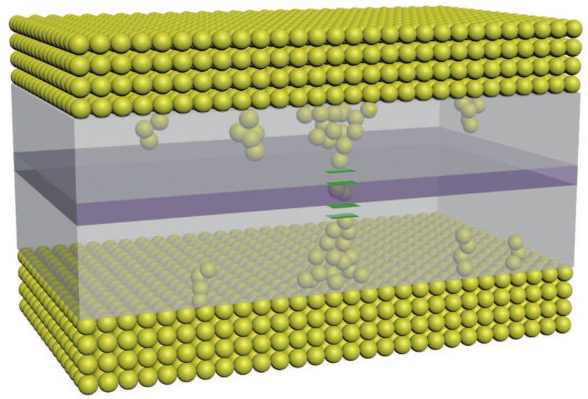
Li Q J, et al. Sci China Inf Sci April 2021 Vol. 64 142402:3
(a) First sweep (b)
10−4 Second sweep 10−4
Third sweep
10−5 10−5
10−6 10−6
Current (A)
Current (A)
10−7 10−7
10−8 10−8
Selectivity>105
10−9 10−9
10−10 10−10
10 −11
10−11
−1.0 0 1.0 −1.0 0 1.0
Voltage (V) Voltage (V)
10−10
(c) (d)
10−4
10−5
10−6
Current (A)
Current (A)
10−7 10−11
slope < 2 mv/dec
10−8
10−9
10−10
10−11 10−12
−0.4 0 0.4 0 2000 4000 6000 8000 10000
Voltage (V) Time (s)
Figure 2 (Color online) DC sweep characteristics. (a) Bidirectional threshold switching phenomena under various compliance
currents. (b) Volatile threshold switching with high selectivity. (c) Low switching slope. (d) DC stress test under a 0.2-V bias.
Time (µs)
0 5 10
3 0 0
200
Voltage (V)
Current (μA)
Current (μA)
2
Voltage (V)
−1
35 ns
30 ns
1 −2
−200
0 0 −3
0 5 10
Time (µs)
(b)
(a)
2
3 3 200
Voltage (V)
Current (μA)
2 2
1
Turn ON Turn OFF
1 1
0 0 0 0
0 10 0 200 210 220
Time (µs) Time (µs) Time (µs)
(c)
Figure 3 (Color online) Transient tests. (a) Positive pulse test with a 2-µs delay before threshold switching. (b) Negative pulse
test with a 3-µs delay before switching. (c) Double-pulse test in which the device turns on and off.
Minimizing the interfacial energy between the Ag filament and the dielectric served as the driving force
for the relaxation dynamics of the PMC selector [28]. Once the voltage is removed, the Ag atoms begin to
Li Q J, et al. Sci China Inf Sci April 2021 Vol. 64 142402:4
(a) 100 (b)
10−4 P-Vth
P-Vhold
Cumulative probability (%)
−5
10
N-Vth
10−6 N-Vhold
Current (A)
10−7 μ=0.4022
μ=0.0136 σ=0.0179
10−8 σ=0.0141
10−9 μ=−0.4529
σ=0.0286 μ=−0.0233
−10
10 σ=0.0224
10−11
0
10−12
−1.0 0 1.0 −1.0 0 1.0
Voltage (V) Voltage (V)
109 109
(c) (d)
108 10 MΩ
108
107 107
Resistance (Ω)
Resistance (Ω)
106 Ron 106
Roff
105 105 1 ms 1 ms
0.5 V
4
10 104
103 103
104 105 106 104 105 106
Cycles Cycles
Figure 4 (Color online) Endurance test. (a) DC sweep of 100 cycles with threshold switching in both polarities. (b) Cumulative
probability of the threshold voltage and hold voltage in DC sweeps. (c) A total of 106 pulse tests with a large on/off resistance
difference. (d) A 10-MΩ resistor test with the same pulse applied in the selector test.
slowly diffuse to their minimum energy positions, and the filament is ruptured, with the selector turning
off. It is deduced that the Ag atoms require a long duration to relax to the lowest energy position in
SiTe [28]; thus, other materials with higher mobilities may be examined to improve the relaxation time.
Endurance is another important parameter for selectors, as they are frequently switched to support
the read and write operations of RRAM. Here, the endurance of the as-fabricated devices was evaluated
via repeated DC sweeps and set/reset pulse trains. As shown in Figure 4(a), the device maintains high
uniformity within ± 1 V over 100 repeated DC sweeps. Detailed parameter statistics [average values (µ)
and variance (σ)] are shown in Figure 4(b). Notably, the variances of the positive and negative thresholds
are limited (σ < 0.05), which will benefit large-dimension array applications. Figure 4(c) presents results
from an endurance test with a specifically designed rectangular pulse that guarantees operation without
degrading the device. For more than 106 repeated programming cycles, the device continually switched
to off- and on-states. The off-state shows obvious fluctuations; thus, it is deduced that the accuracy of
the instrument is not sufficient for a low-current test, which was verified by a 10-MΩ standard resistor
test, as shown in Figure 4(d).
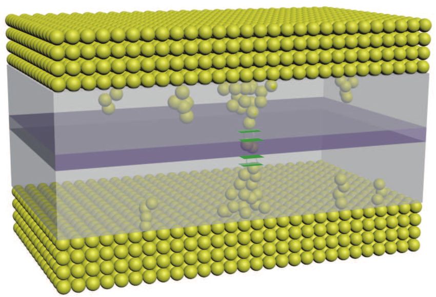
Although we have not fully characterized the in situ structure and material, we assume that the
mechanism is similar to the unipolar mechanisms observed in our previous publications [22]; moreover,
similar phenomena have been observed in other studies [28,29]. A detailed model of bidirectional threshold
switching is illustrated in Figure 5. During the electroforming process for positive and negative voltages
(Figure 5(b)), two Ag protrusions from both the top and bottom Ag electrodes extend to SiTe and HfO2 .
After the voltage is removed, the Ag atoms return to the initial positions with a lower interface energy,
and a narrow gap forms. The HfO2 layer was grown by atom layer deposition with few boundary defects,
leading to a lower mobility of Ag atoms in HfO2 than in SiTe; thus, the filament ruptures in the SiTe
layer near the interface, as shown in Figure 5(d). Subsequently, the connection and rupture of CFs is
limited to the region of face-to-face Ag protrusions, which leads to low voltage variations with volatile
switching properties.
To verify the capability of the as-fabricated bidirectional selector to suppress the sneak current in a
Li Q J, et al.       Sci China Inf Sci                  April 2021 Vol. 64 142402:5

                                         Ag

                                         SiTe                                                                   gap       filament
                                         HfO2

                                         SiTe

                                         Ag
                                                            (a)                                                  (b)

                                                            filament                                             gap       filament

                                                            (c)                                                           (d)

Figure 5 (Color online) Mechanism analysis. (a) Initial state with a few Ag atoms doped during fabrication. (b) Conductive
filaments are formed when a voltage is applied, and the filaments automatically rupture after the voltage is removed, with only
a small gap remaining. (c) Residual filaments provide a preferred path for filament reformation when a voltage is applied again.
(d) Ag atoms return to the minimum interfacial energy position after the voltage is removed, and filaments in the SiTe layer near
the interface rupture.

                         10−4      (a)                                                                    (b)
                                                                                                10−4
                         10−5                                                                   10−5
                                                                       1R                                                                     1S1R
                              −6
                         10                                                                     10−6
           Current (A)

                                                                                  Current (A)

                         10−7                                                                   10−7
                            −8
                         10                                                                     10−8
                         10   −9
                                                                                                10−9                  3      4        2   1
                         10−10                                                                  10−10

                         10−11                                                                  10−11
                         10−12                                                                  10−12
                            −4.0                   0                        4.0                    −4.0                           0                  4.0
                                              Voltage (V)                                                                   Voltage (V)

Figure 6 (Color online) DC characteristics for 1R (a) and 1S1R (b). The cell current is suppressed by the selector when the
voltage is lower than the threshold voltage.

bipolar RRAM array, the device was integrated with a TiN/NbOx /Pt RRAM device, forming a wire-
connected 1S1R cell. As shown in Figure 6(a), the device shows weak self-rectifying characteristics, with
a rectification ratio of 50 at ± 1 V. In the positive domain, the high resistance is approximately 2 MΩ,
and the low resistance is approximately 200 kΩ, with a 10x window of HRS/LRS. Meanwhile, a switching
current of 10 µA is suitable for integration with the selector. As shown in Figure 6(b), during the first
positive sweep “1” (0 → 4 V), the selector turns to the on-state at approximately 1 V, and the memory
turns to the on-state at approximately 1.91 V with a slight jump. With the subsequent back sweep “2”
(4 V→ 0), the current is larger than the initial current, indicating that the SET is successful. Once the
voltage is lower than 0.34 V, the selector turns off. During the negative biasing sweep “3”, the selector
turns to the on-state at approximately −1.13 V, and the memory then shows rectifying behavior. During
the following negative sweep back “4”, the cell turns off at −0.29 V. This successful positive and negative
cycle indicates that the bidirectional Ag/SiTe/HfO2 /SiTe/Ag selector can restrain the sneak path current
in a large memory array.

4    Conclusion
In summary, we have fabricated a symmetric multilayer programmable metallization selector with an
Ag/SiTe/HfO2 /SiTe/Ag structure. The device demonstrates bidirectional threshold switching character-
istics with a low off current (< 10−10 A) and a high selectivity (> 105 ). It is deduced that due to the
Li Q J, et al. Sci China Inf Sci April 2021 Vol. 64 142402:6
mobility difference for Ag atoms in SiTe and HfO2 , residual filaments can reduce the threshold voltage
variation (< 0.05). In addition, a suitable self-rectifying memristor with a switching current of 10 µA was
integrated with the as-fabricated device to determine its ability to the suppress the leakage current. The
turn-off time can be minimized by optimizing the selector materials and structures. This method can be
applied for bidirectional selector improvements and may pave the way for high-density 1S1R arrays.
Acknowledgements This work was supported by National Natural Science Foundation of China (Grant Nos. 61604177, 61704191,
61471377).
References
1 Lastras-Montaño M A, Cheng K T. Resistive random-access memory based on ratioed memristors. Nat Electron, 2018, 1:
466–472
2 Lee S, Song J, Seong C, et al. Full chip integration of 3-D cross-point ReRAM with leakage-compensating write driver and
disturbance-aware sense amplifier. In: Proceedings of Symposium on VLSI Circuits Digest of Technical Papers, Honolulu,
2016
3 Li Y, Long S B, Liu Q, et al. Resistive switching performance improvement via modulating nanoscale conductive filament,
involving the application of two-dimensional layered materials. Small, 2017, 13: 1604306
4 Yao P, Wu H Q, Gao B, et al. Fully hardware-implemented memristor convolutional neural network. Nature, 2020, 577:
641–646
5 Zidan M A, Jeong Y J, Lee J, et al. A general memristor-based partial differential equation solver. Nat Electron, 2018, 1:
411–420
6 Nili H, Adam G C, Hoskins B, et al. Hardware-intrinsic security primitives enabled by analogue state and nonlinear conduc-
tance variations in integrated memristors. Nat Electron, 2018, 1: 197–202
7 Sun Z, Pedretti G, Bricalli A, et al. One-step regression and classification with cross-point resistive memory arrays. Sci Adv,
2020, 6: 2378
8 Chen A. Accessibility of nano-crossbar arrays of resistive switching devices. In: Proceedings of the 11th IEEE Conference on
Nanotechnology, Portland, 2011
9 Chen A, Lin M R. Variability of resistive switching memories and its impact on crossbar array performance. In: Proceedings
of IEEE International Reliability Physics Symposium, Monterey, 2011
10 Gao S, Zeng F, Wang M J, et al. Implementation of complete Boolean logic functions in single complementary resistive switch.
Sci Rep, 2015, 5: 15467
11 Gao S, Zeng F, Li F, et al. Forming-free and self-rectifying resistive switching of the simple Pt/TaOx /n-Si structure for access
device-free high-density memory application. Nanoscale, 2015, 7: 6031–6038
12 Chen F T, Chen Y S, Wu T Y, et al. Write scheme allowing reduced LRS nonlinearity requirement in a 3D-RRAM array with
selector-less 1TNR architecture. IEEE Electron Device Lett, 2014, 35: 223–225
13 Chasin A, Zhang L, Bhoolokam A, et al. High-performance a-IGZO thin film diode as selector for cross-point memory
application. IEEE Electron Device Lett, 2014, 35: 642–644
14 Burr G W, Shenoy R S, Virwani K, et al. Access devices for 3D crosspoint memory. J Vacuum Sci Tech B, 2014, 32: 040802
15 Huang C H, Matsuzaki K, Nomura K. Threshold switching of non-stoichiometric CuO nanowire for selector application. Appl
Phys Lett, 2020, 116: 023503
16 Lee T H, Kang D Y, Kim T G. Ag:SiOx Ny -based bilayer ReRAM structure with self-limiting bidirectional threshold switching
characteristics for cross-point array application. ACS Appl Mater Int, 2018, 10: 33768–33772
17 Song B, Xu H, Liu S, et al. An ovonic threshold switching selector based on Se-rich GeSe chalcogenide. Appl Phys A, 2019,
125: 772
18 Noé P, Verdy A, d’Acapito F, et al. Toward ultimate nonvolatile resistive memories: the mechanism behind ovonic threshold
switching revealed. Sci Adv, 2020, 6: 2830
19 Saitoh S, Kinoshita K. Oxide-based selector with trap-filling-controlled threshold switching. Appl Phys Lett, 2020, 116:
112101
20 Chen A, Ma G, Zhang Z, et al. Multi-functional controllable memory devices applied for 3D integration based on a single
niobium oxide layer. Adv Electron Mater, 2020, 6: 1900756
21 Song B, Xu H, Liu S, et al. Threshold switching behavior of Ag-SiTe-based selector device and annealing effect on its
characteristics. IEEE J Electron Device Soc, 2018, 6: 674–679
22 Song B, Cao R R, Xu H, et al. A HfO2 /SiTe based dual-layer selector device with minor threshold voltage variation.
Nanomaterials, 2019, 9: 408
23 Song J, Park J, Moon K, et al. Monolithic integration of AgTe/TiO2 based threshold switching device with TiN liner for
steep slope field-effect transistor. In: Proceedings of IEEE International Electron Devices Meeting, San Francisco, 2016
24 Zhang L Q, Cosemans S, Wouters D J, et al. One-selector one-resistor cross-point array with threshold switching selector.
IEEE Trans Electron Device, 2015, 62: 3250–3257
25 Song B, Xu H, Liu H J, et al. Impact of threshold voltage variation on 1S1R crossbar array with threshold switching selectors.
Appl Phys A, 2017, 123: 356
26 Liu S, Lu N D, Zhao X L, et al. Eliminating negative-SET behavior by suppressing nanofilament overgrowth in cation-based
memory. Adv Mater, 2016, 28: 10623–10629
27 Zaffora A, Cho D Y, Lee K S, et al. Electrochemical Tantalum Oxide for resistive switching memories. Adv Mater, 2017, 29:
1703357
28 Zhao X L, Ma J, Xiao X H, et al. Breaking the current-retention dilemma in cation-based resistive switching devices utilizing
graphene with controlled defects. Adv Mater, 2018, 30: 1705193
29 Ji X L, Song L, He W, et al. Super nonlinear electrodeposition-diffusion-controlled thin-film selector. ACS Appl Mater
Interface, 2018, 10: 10165–10172You can also read