AC-DC Non-Isolated SMPS for Single Phase Smart Meters Based on UCC28722
←
→
Page content transcription
If your browser does not render page correctly, please read the page content below
Application Report
                                                                                                           SLUA721 – June 2014

  AC-DC Non-Isolated SMPS for Single Phase Smart Meters
                                    Based on UCC28722

Harmeet Singh, Salil Chellappan, Sanjay Dixit ....................................................................... Power Stage

                                                                ABSTRACT
       Single phase prepaid/smart meters need very low cost, low wattage (< 2.5 W) non-isolated power supply.
       The meters should be capable of working with an input voltage range of 100 VAC on the lower side, given
       poor utility conditions in some regions, to 415 VAC on the higher side so as to sustain phase-phase
       voltage as well. The real voltage levels can touch 500 VAC (415 VAC +20%).
       The application report describes an innovative application of the UCC28722 flyback controller used in a
       buck configuration tailored for a smart energy metering application. This serves as superior alternative to
       existing power supplies with integrated MOSFET technology. The following list shows the benefits:
       • Works for a wide input range (110 VAC–500 VAC)
       • Uses lowest cost BJT making the overall solution cheap
       • High conversion efficiency because of combination of frequency and peak current modulation
       • Ultra low standby power of 75 mW
       • Features drum core inductor for smallest form factor
       This application report goes through the step-by-step procedures a designer must follow to complete an
       AC-DC Buck switch mode power supply unit (SMPS) using the UCC28722.The board has been built and
       tested based on this application report and is available for download as PMP6778 on www.ti.com.

                            Figure 1. AC-DC Buck Design Using UCC28722 (PMP6778)

       spacer
       spacer
       spacer
       spacer

SLUA721 – June 2014                                         AC-DC Non-Isolated SMPS for Single Phase Smart Meters Based on     1
Submit Documentation Feedback                                                                                   UCC28722
                                            Copyright © 2014, Texas Instruments Incorporated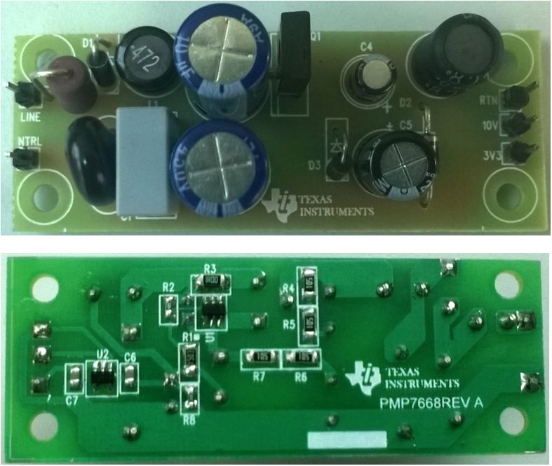
www.ti.com

                                                                 Contents
    1     SMPS Design Specifications ............................................................................................... 3
    2     Basic Principle of Buck Topology .......................................................................................... 3
          2.1      Buck Steady-State Discontinuous Conduction Mode Analysis ............................................... 4
    3     Step-by-Step Design Procedure of UCC28722-Based Buck Converter .............................................. 7
          3.1      AC Input Stage Components ..................................................................................... 7
          3.2      Feedback Resistors ................................................................................................ 7
          3.3      VDD Capacitance .................................................................................................. 8
          3.4      Startup Resistors and Startup Time .............................................................................. 8
          3.5      Current Sense Resistor ............................................................................................ 9
          3.6      Output Inductor .................................................................................................... 10
          3.7      Freewheeling Diode and Vdd Diode ............................................................................ 10
          3.8      Output Capacitor .................................................................................................. 10
          3.9      Bipolar Junction Transistor ....................................................................................... 11
          3.10 LDO for 3.3 V ...................................................................................................... 12
    4     Bill of Materials ............................................................................................................. 13
    5     PCB Details ................................................................................................................. 14
    6     Conclusion .................................................................................................................. 15
    7     References .................................................................................................................. 15
    Appendix A     Experimental Results ............................................................................................. 16

                                                                List of Figures
    1       AC-DC Buck Design Using UCC28722 (PMP6778)                   ....................................................................    1
    2       Buck Power Stage Schematic.............................................................................................. 3
    3       Buck Power Stages in Discontinuous Mode             .............................................................................   5
    4       Discontinuous Mode Power Stage Buck Waveforms ................................................................... 6
    5       Timing Diagram of Startup Sequence in UCC28722.................................................................... 8
    6       Discontinuous Current Waveform in UCC28722               ........................................................................   9
    7       Complete Schematic of the PMP7668 Non-Isolated Buck Converter ............................................... 12
    8       PCB Top Silk Screen ...................................................................................................... 14
    9       PCB Bottom Silk Screen       ..................................................................................................     14
    10      PCB Composite Layout .................................................................................................... 14
    11      Efficiency vs AC I/p Voltage (110 V–275 V) ............................................................................ 16
    12      Efficiency vs DC I/p Voltage (400 V–705 V) ............................................................................ 16
    13      Efficiency vs O/p Load Current at 325 VDC ............................................................................ 17
    14      O/p Voltage Variation vs O/p Load Current at 325 VDC .............................................................. 17
    15      SW Node Waveform and Collector Current at Vin = 110 VAC, Full Load .......................................... 18
    16      Zoomed SW Waveform and Collector Current at Vin = 110 VAC, Full Load....................................... 18
    17      SW node Waveform and Collector Current at Vin = 275 VAC, Full Load           ..........................................             19
    18      Zoomed SW Waveform and Collector Current at Vin = 275 VAC, Full Load.......................................                         19
    19      Vout Ripple at Vin = 110 VAC, Full Load ...............................................................................             20
    20      Vout Ripple at Vin = 275 VAC, Full Load ...............................................................................             20
    21      Vout Turn On Waveform at Vin = 110 VAC, Full Load ................................................................                  21
    22      Vout Turn On Waveform at Vin = 275 VAC, Full Load ................................................................                  22
    23      Vout Waveform at Vin = 230 VAC, Load Transient from 2 mA to 200 mA .........................................                        23
    24      Conducted Emissions as per EN55022 Class B .......................................................................                  24

                                                                List of Tables
    1       AC-DC Non-Isolated Single Phase Smart Meter SMPS Design Specifications ..................................... 3
    2       Bill of Materials of Complete Schematic................................................................................. 13

2   AC-DC Non-Isolated SMPS for Single Phase Smart Meters Based on                                                    SLUA721 – June 2014
    UCC28722                                                                                                Submit Documentation Feedback
                                             Copyright © 2014, Texas Instruments Incorporated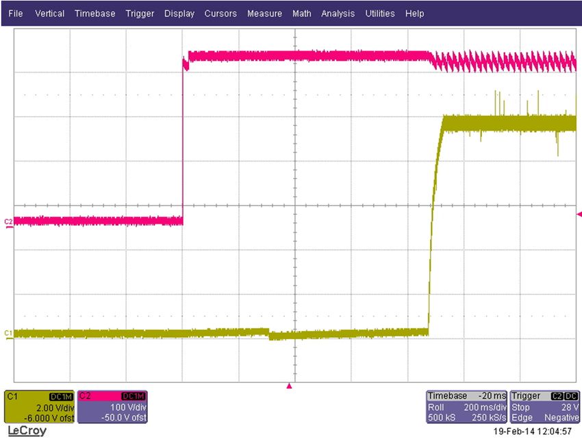
www.ti.com                                                                                                  SMPS Design Specifications

1       SMPS Design Specifications

                     Table 1. AC-DC Non-Isolated Single Phase Smart Meter SMPS Design Specifications
         The main specifications of the SMPS are listed below:
         Input
         Voltage                    110–500 VAC
         Frequency                  48–52 Hz
         Output
                                    10 V ±1 V
                                    3.3 V ±1%
                                    200 mA output current on 10 V and 2 mA on 3.3 V for full input voltage range
         Standby Power(W/VA)        < 75 mW/300 mVA at 240 VAC (2 mA on 3.3 V and no load on 10 V)
         Efficiency                 > 65%
         Overload/Short-circuit     Protected
         Output overvoltage         Protected
         PCB type and size
                                    FR4
                                    Single sided 35 μm
                                    69 mm × 26 mm
         Isolation                  Non isolated - N connected to output GND
         EMI                        In accordance with EN55022 - class B
         EMC                        Surge - IEC 61000-4-5 - 4kV
         EMC                        EFT - IEC 61000-4-4 - 4kV

2       Basic Principle of Buck Topology
        Figure 2 shows a simplified schematic of the buck power stage with a drive circuit block included. The
        power switch, Q1, is a NPN bipolar transistor. The diode, D1, is usually called the freewheeling diode. The
        inductor, L, and capacitor, C1, make up the output filter. Resr represents the capacitor ESR and RL
        represents the inductor DC resistance. The resistor, RLoad, represents the load seen by the power stage
        output.

                                             Figure 2. Buck Power Stage Schematic

        During normal operation of the buck power stage, Q1 is repeatedly switched on and off with the on and off
        times governed by the control circuit. This switching action causes a train of pulses at the junction of Q1,
        D1, and L which is filtered by the L/C1 output filter to produce a DC output voltage, Vo.

All trademarks are the property of their respective owners.

SLUA721 – June 2014                                              AC-DC Non-Isolated SMPS for Single Phase Smart Meters Based on      3
Submit Documentation Feedback                                                                                        UCC28722
                                                 Copyright © 2014, Texas Instruments Incorporated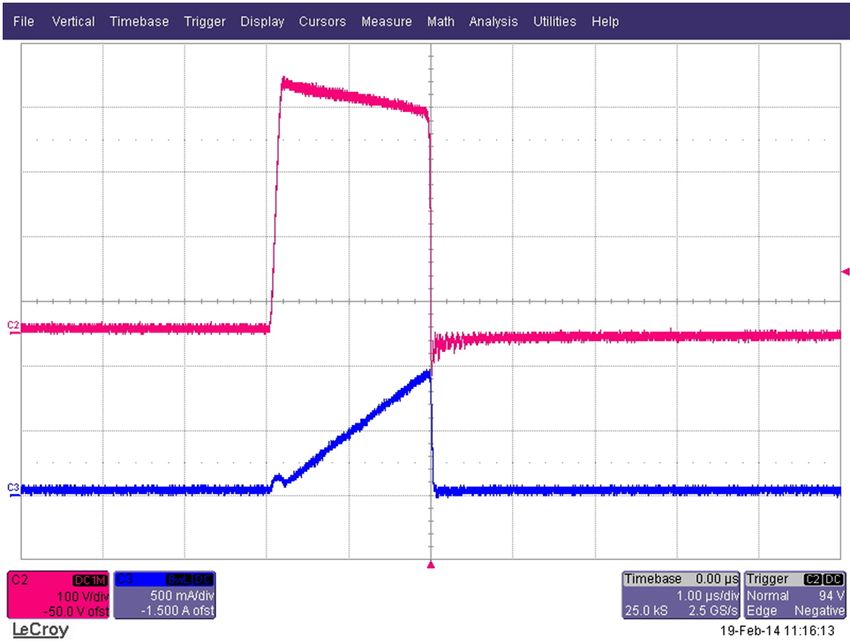
Basic Principle of Buck Topology                                                                               www.ti.com

       A power stage can operate in continuous or discontinuous inductor current mode. Continuous inductor
       current mode is characterized by current flowing continuously in the inductor during the entire switching
       cycle in steady-state operation. Discontinuous inductor current mode is characterized by the inductor
       current being zero for a portion of the switching cycle. It starts at zero, reaches a peak value, and returns
       to zero during each switching cycle. It is very desirable for a power stage to stay in only one mode over its
       expected operating conditions, because the power stage frequency response changes significantly
       between the two modes of operation.

2.1    Buck Steady-State Discontinuous Conduction Mode Analysis
       The following is a description of steady-state operation in discontinuous conduction mode – as UCC28722
       operates only in this mode. A power stage operating in discontinuous conduction mode has three unique
       states during each switching cycle, shown in Figure 2. The ON state is when Q1 is ON and D1 is OFF.
       The OFF state is when Q1 is OFF and D1 is ON. The IDLE state is when both Q1 and D1 are OFF A
       simple linear circuit can represent each of the three states where the switches in the circuit are replaced
       by their equivalent circuits during each state. The circuit diagram for each of the three states is shown in
       Figure 3.
       The duration of the ON state is TON = D × TS where D is the duty cycle, set by the control circuit,
       expressed as a ratio of the switch ON time to the time of one complete switching cycle, Ts . The duration
       of the OFF state is TOFF = D2 × TS. The IDLE time is the remainder of the switching cycle and is given
       as TS – TON – TOFF = D3 × TS. These times are shown with the waveforms in Figure 4.
       The main result of this section is a derivation of the voltage conversion relationship for the discontinuous
       conduction mode buck power stage. In addition, the dc resistance of the output inductor, the output diode
       forward voltage drop, and the power BJT Vce drop are all assumed to be small enough to omit in analysis.
       Referring to Figure 3, during the ON state, the voltage applied to the right-hand side of L is simply the
       output voltage, Vo. The inductor current, IL, flows from the input source, VI, through Q1 and to the output
       capacitor C1 and load resistor RLoad combination. During the ON state, the voltage applied across the
       inductor is constant and equal to VI – Vo. Adopting the polarity convention for the current IL shown in
       Figure 3, the inductor current increases as a result of the applied voltage. Also, since the applied voltage
       is essentially constant, the inductor current increases linearly. This increase in inductor current during
       TON is illustrated in Figure 4.
       The amount that the inductor current increases can be calculated by using a version of the familiar
       relationship:
                      diL         VL
             VL = L ´     ® DIL =    ´ DT
                      dt          L                                                                                    (1)
       The inductor current increase during the ON state is given by:
                       VI - Vo         VI - Vo
            DIL( + ) =         ´ Ton =         ´ D ´ Ts = IPK
                          L               L                                                                            (2)
       The ripple current magnitude, ΔIL (+), is also the peak inductor current, IPK.

4      AC-DC Non-Isolated SMPS for Single Phase Smart Meters Based on                                  SLUA721 – June 2014
       UCC28722                                                                              Submit Documentation Feedback
                                          Copyright © 2014, Texas Instruments Incorporated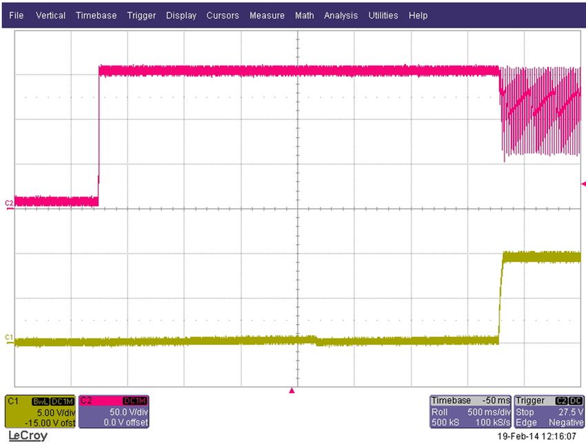
www.ti.com                                                                                   Basic Principle of Buck Topology

                                Figure 3. Buck Power Stages in Discontinuous Mode

       Referring to Figure 3, when Q1 is OFF, it presents high impedance from its collector to emitter. Therefore,
       since the current flowing in the inductor L cannot change instantaneously, the current shifts from Q1 to D1.
       Due to the decreasing inductor current, the voltage across the inductor reverses polarity until rectifier D1
       becomes forward biased and turns ON. The voltage on the left-hand side of L becomes zero if we neglect
       the forward voltage drop of diode D1 and the drop across DC resistance of the inductor. The voltage
       applied to the right-hand side of L is still the output voltage, Vo. The inductor current, IL, now flows from
       ground through D1 and to the output capacitor C1 and load resistor RLoad combination. During the OFF
       state, the magnitude of the voltage applied across the inductor is constant and equal to Vo. Maintaining
       our same polarity convention; this applied voltage is negative (or opposite in polarity from the applied
       voltage during the ON time). Hence, the inductor current decreases during the OFF time. Also, since the
       applied voltage is essentially constant, the inductor current decreases linearly. This decrease in inductor
       current during TOFF is illustrated in Figure 4.
       The inductor current decrease during the OFF state is given by:
                       Vo
            DIL (- ) =    ´ TOFF
                       L                                                                                                  (3)
       This quantity, ΔIL (–), is also referred to as the inductor ripple current.
       In steady state conditions, the current increase, ΔIL (+), during the ON time and the current decrease
       during the OFF time, ΔIL(–), must be equal. Otherwise, the inductor current would have a net increase or
       decrease from cycle to cycle which would not be a steady state condition. Therefore, Equation 2 and
       Equation 3 can be equated and solved for Vo to obtain the first of two equations to be used to solve for
       the voltage conversion ratio:
                            TON                   D
             Vo = VI ´                 = VI ´
                        TON + TOFF              D + D2                                                          (4)
       Now we calculate the output current (the output voltage Vo divided by the output load RLoad). It is the
       average of the inductor current.

SLUA721 – June 2014                                      AC-DC Non-Isolated SMPS for Single Phase Smart Meters Based on    5
Submit Documentation Feedback                                                                                UCC28722
                                         Copyright © 2014, Texas Instruments Incorporated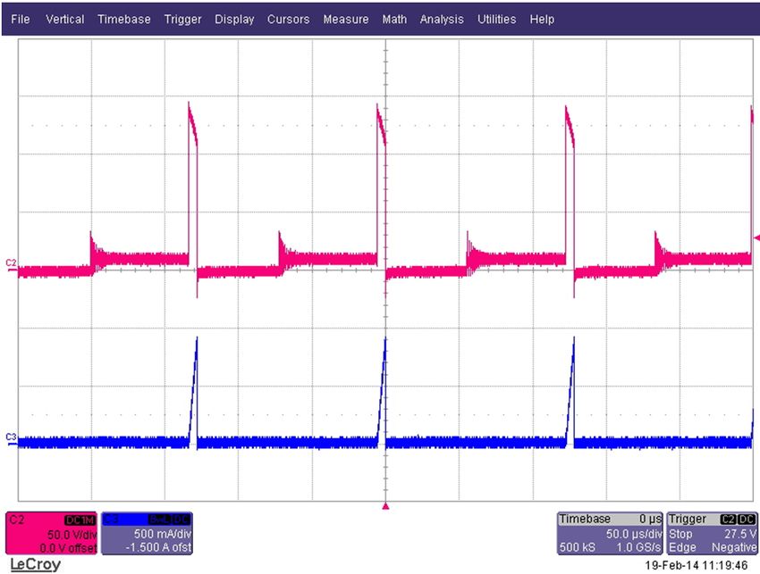
Basic Principle of Buck Topology                                                                               www.ti.com

                               Vo     IPK   D ´ Ts + D2 ´ Ts
            Io = IL (avg) =         =     ´
                              RLoad    2          Ts                                                                   (5)
       Now, substitute the relationship for IPK into the above equation to obtain:
                    Vo                       D ´ Ts
           Io =            = (VI - Vo ) ´           ´ (D + D2 )
                  RLoad                       2´L                                                                      (6)
       We now have two equations, the one for the output current just derived and the one for the output voltage
       (above), both in terms of VI, D, and D2. We now solve each equation for D2 and set the two equations
       equal to each other. Using the resulting equation, an expression for the output voltage, Vo, can be
       derived.
       The discontinuous conduction mode buck voltage conversion relationship is given by:
                             2
            Vo = VI ´
                              4 ´ K
                       1+ 1+
                               D2                                                                                      (7)
       Where K is defined as:
                    (2   ´ L)
            K=
                 RLoad ´ Ts                                                                                            (8)

                                IQ1                                                          IPK

                                Id1                                                          IPK

                            IL Solid
                                                                                               IL
                          IO Dashed

                         VSW Solid
                         VO Dashed

                                                      D x TS
                                                                D2 x TS

                                                                           TS

                           Figure 4. Discontinuous Mode Power Stage Buck Waveforms

6      AC-DC Non-Isolated SMPS for Single Phase Smart Meters Based on                                  SLUA721 – June 2014
       UCC28722                                                                              Submit Documentation Feedback
                                          Copyright © 2014, Texas Instruments Incorporated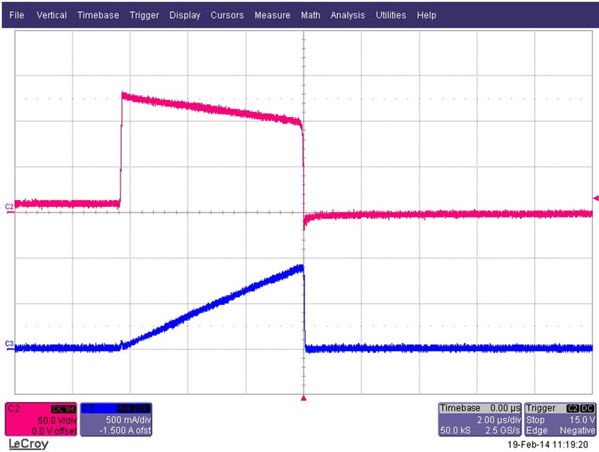
www.ti.com                                              Step-by-Step Design Procedure of UCC28722-Based Buck Converter

3      Step-by-Step Design Procedure of UCC28722-Based Buck Converter
       We will be referring to Figure 6 for discussion on choosing the various components for the design.

3.1    AC Input Stage Components
       The input stage consists of fusible resistance FR1, Varistor RT1, input rectification diode D1, the line filter
       network L1/ C1 and the main bulk electrolytic capacitors C2 and C3.
       The input resistance FR1 provides three important functions:
       • Acts as a fuse in case of any short in the power supply
       • Controls the inrush current going into bulk capacitors
       • Aids in differential mode attenuation
       As it has to perform these three functions so flame proof and film type resistance or WWR surge
       resistance is recommended.
       For designs up to 2 W of output power, 8.2–10 Ω 3 W is recommended for FR1.
       Regulation IEC 61000-4-5 defines the surge immunity test as high power spikes caused by large inductive
       devices in mains. The input of the SMPS is coupled by a short duration (1.2/50 μs) pulses but high voltage
       (up to 4 kV). The pulses are applied between L-N and between L (N) – PE at different angles 0°, 90°,
       180°, 270°, 360° of the ac voltage. For the energy meter it is applied between L-N as there is no earth.
       The surge pulse causes high inrush current, quickly charging the storage capacitor in a standard SMPS.
       The major risk is overvoltage for input components - bulk capacitors, rectifier diode and the main BJT
       switch. The inrush current can damage the components- rectifier diode, fusible resistance in series in the
       input section. Typically, the varistors are used to absorb part of the energy and the rest is absorbed by the
       bulk capacitors used.
       As the input AC voltage can go as high as 500 VAC, so a 510 VAC, 10-mm varistor RT1 is recommended
       for the design for surges up to the 4-kV level. If the application requires surge immunity up to higher levels
       than appropriate values and diameter of the varistor along with the input resistance should be chosen.
       This topic is beyond the scope of this application note.
       As the output ground of the system will be same as the input neutral in case of energy meters, a half-
       wave rectifier comprising of D1, C2 and C3 are used. As the input AC voltage can go up to 500 VAC, so
       the DC voltage can reach voltage levels of up to 707 VDC. The input bulk capacitor must be able to
       sustain such voltage levels. There are no standard aluminum capacitors in the market suitable for this
       voltage, so two capacitors connected in series have been used. For a half-wave rectifier, choose net
       capacitance between 6–8 µF per Watt of output power. Keeping the cost and size in mind, C2 = C3 = 10
       µF 400-V capacitors are chosen. TI recommends 1 A, 1000 V, 1N4007 for D1.
       L1 and C1 form a differential filter attenuating the differential noise produced by the UCC28722-based
       buck converter. The recommended value for L1 is 2.2–4.7 mH and C1 is 47–100 nF.

3.2    Feedback Resistors
       The VS divider resistors R1 and R2 determine the output voltage regulation point of the buck converter.
       The high-side divider resistor (R1) determines the line voltage at which the controller enables continuous
       DRV operation. R1 is initially determined based on desired input voltage operating threshold.
                    VINmin ´ 2
             R1 =
                      IVSL(run)                                                                                          (9)
       Where
         VINmin is the AC RMS voltage to enable turn-on of the controller (run),
         IVSL(run) is the run-threshold for the current pulled out of the VS pin during the switch on time
       Keep the impedance at Vs pin low, < 100 kΩ, so as to be not effected by switching noise. So substituting
       VINmin as 25 VAC instead of 100 VAC and IVSL (run) as 225 µA, R1 comes out to be 157 kΩ. A standard
       value of 150 kΩ is chosen.
       The low-side VS pin resistor R2 is selected based on desired Vo regulation voltage.

SLUA721 – June 2014                                     AC-DC Non-Isolated SMPS for Single Phase Smart Meters Based on    7
Submit Documentation Feedback                                                                               UCC28722
                                        Copyright © 2014, Texas Instruments Incorporated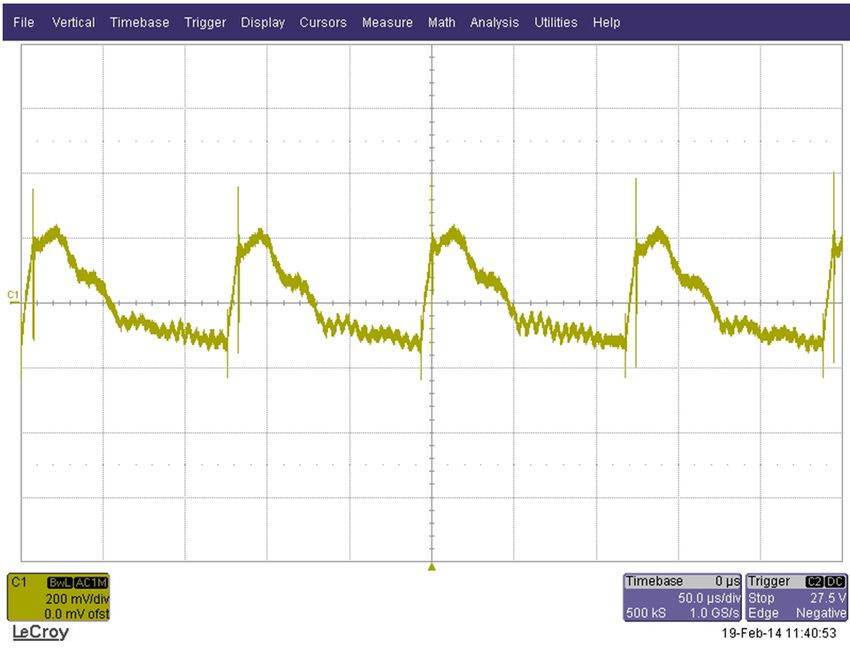
Step-by-Step Design Procedure of UCC28722-Based Buck Converter                                                                            www.ti.com

                    R1 ´ VVSR
           R2 =
                  (Vo + VF ) - VVSR                                                                                                              (10)
      Where
        Vo is the converter regulated output voltage,
        VF is the output rectifier forward drop at near-zero current,
        R1 is the VS divider high-side resistance,
        VVSR is the CV regulating level at the VS input
      Substituting Vo as 10 V, VF as 0.7 V, R1 as 150 kΩ, and VVSR as 4.05 V, we get R2 as 91 kΩ so
      standard value of 100 kΩ is chosen.

3.3   VDD Capacitance
      The capacitance C4 on VDD needs to supply the device operating current until the output of the converter
      reaches the target minimum operating voltage in constant-current regulation. At this time, the output
      voltage can sustain the voltage to the UCC28722. The total output current available to the load and to
      charge the output capacitors is the constant-current regulation target, IOCC. Equation 11 is used to
      calculate the value of Capacitance required at the VDD pin:
                                                                C5 ´ Vo
                  æ        æ                 Vo      öö            Iocc
           Cdd = çç Irun + ç Idrsmax ´               ÷ ÷÷ ´
                  è        è           VINmin ´ 2 ø ø (     Vddon - Vddoff - 1V )                            (11)
      Where
        Idrsmax is the maximum driver source current
        Vddoff is the UVLO turn-off voltage
        Vddon is the UVLO turn-on voltage
        C5 is the output capacitor used
        Irun is the supply current in run state with Idrv = 0
      Substituting Irun as 2.65 mA, Idrsmax as 41 mA, Vo as 10 V, VINmin as 100 V, C5 as 220 µF, Iocc as
      220 mA, Vddon as 21 V, and Vddoff as 8 V we get Cdd as 4.58 µF. So a standard value of 4.7 uF is
      chosen. The timing diagram illustrating the startup of UCC28722 is shown in Figure 5.
                                                                                                       Vo
                                     Vcc                                         Irun + Idrsmax x
                                            Design                                                  VINminxÖ2
                                            Margin

                       UVLOhigh (21 V)
                                             Iv                                                                    DV

                        UVLOlow (8 V)

                                                  Istr                         O/p Voltage                      Power Supply
                                                                               Takes Over                       Regulates

                                                  t1                      t2

                                                         Total Startup Time

                          Figure 5. Timing Diagram of Startup Sequence in UCC28722

3.4   Startup Resistors and Startup Time
      An external resistor connected from the bulk capacitor voltage to the VDD pin charges the VDD capacitor.
      The amount of startup current that is available to charge the VDD capacitor is dependent on the value of
      this external startup resistor. Smaller values supply more current and decrease startup time but at the
      expense of increasing standby power and decreasing efficiency, particularly at high input voltage and light
      loading.

8     AC-DC Non-Isolated SMPS for Single Phase Smart Meters Based on                                                              SLUA721 – June 2014
      UCC28722                                                                                                          Submit Documentation Feedback
                                           Copyright © 2014, Texas Instruments Incorporated
www.ti.com                                                Step-by-Step Design Procedure of UCC28722-Based Buck Converter

       When VDD reaches the 21-V UVLO turn-on threshold, the controller is enabled and the converter starts
       switching. The initial three cycles are limited to IPP(min). After the initial three cycles at minimum IPP(min), the
       controller responds to the condition dictated by the control law. The converter will remain in discontinuous
       mode during charging of the output capacitor(s), maintaining a constant output current until the output
       voltage is in regulation.
       Once the VDD capacitor is known, there is a tradeoff to be made between startup time and overall
       standby input power to the converter. Faster startup time requires a smaller startup resistance, which
       results in higher standby input power.
                             2 ´ VINmin
             Rstr =
                               VDDon ´ Cdd
                      Istart +
                                   Tstr                                                                                    (12)
       Where:
         VINmin is the minimum voltage at which the converter should work
         Istart is the startup current of UCC28722
         VDDon is the UVLO turn on threshold
         Tstr is the time in which the power supply should be stable at desired O/p voltage
         Cdd is the capacitance value at VDD pin
       Substituting VINmin as 110 V, Istart as 1.5 µA, VDDon as 21 V, Tstr as 3 s, Cdd as 4.7 µF, Rstr comes
       out to be 4.09 MΩ. So we split the required resistance into R4 = R5 = R6 = R7 = 1 MΩ. Splitting the
       resistance into four helps meet the required voltage rating.
       R5 and R6 resistance midpoint is attached to the midpoint of series capacitor C2 and C3 .This concept
       serves to keep the center point of capacitors at exactly half voltage of Vbulk by acting as balancing
       resistors.

3.5    Current Sense Resistor
       During startup, the converter remains in constant current mode charging the output capacitor until it
       comes into voltage loop or regulation. This constant current should be more than the output current
       required in order to charge the o/p capacitor at full load. The inductor and the output current is shown in
       Figure 6 for UCC28722 in buck discontinuous mode.

                            Figure 6. Discontinuous Current Waveform in UCC28722

       Using Equation 5 for calculation of output current in constant current (CC) mode, substituting Io = Iocc, D2
       = toff/T = Dmagcc and ignoring D (ton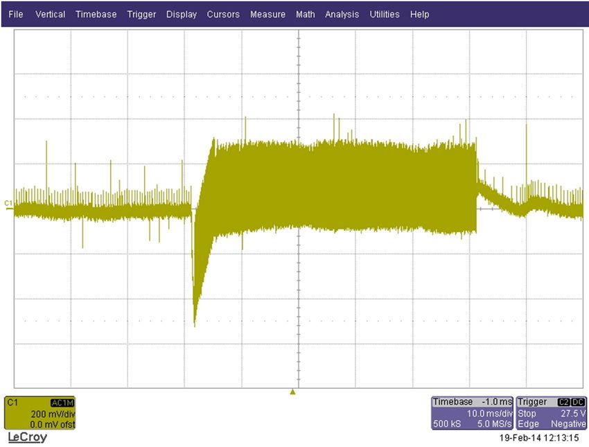
Step-by-Step Design Procedure of UCC28722-Based Buck Converter                                                www.ti.com

      Where
        Iocc is the converter output constant-current target
        Dmagcc is the maximum demagnetization duty cycle
      The UCC28722 constant-current regulation is achieved by maintaining a maximum Dmag duty cycle of
      0.425 at the maximum inductor current setting. Substituting Iocc as 220 mA (10% more than Io) and
      Dmagcc as 0.425, Ipk comes out to be 1.035 A.
      During constant current mode the voltage drop across R3 is maintained at 0.78 V. The current sense
      resistance R3 is calculated using Equation 15.
                 0.78
            R3 =
                 Ipk                                                                                     (15)
      Substituting the Ipk value gives R3 as 0.75 Ω.
      We can estimate the switching frequency during the exit from CC to CV mode during the start up phase.
      Using Equation 3 and substituting ∆IL(-) = IPK and reorganizing the equation, TOFF is given by:
                   IPK
           TOFF =       ´ L
                    Vo                                                                                    (16)
      Substituting IPK as 1.035 A, Vo = 10 V, L = 800 µH, TOFF comes out to be 82.8 µs.
      The switching frequency, Fsw, is given by Equation 17.
                          Dmagcc
           Fsw = 1/ Tsw =
                            TOFF                                                                                     (17)
      Substituting Dmagcc = 0.425 and TOFF as 82.8 µs, Fsw comes out to 5.1 kHz.

3.6   Output Inductor
      The output inductor can be calculated by reshuffling Equation 2 as seen in Equation 18:
                  (Ö 2 ´ VINmax) - Vo
           L2 =                       ´ Ton
                          Ipk                                                                                        (18)
      Now there is an internal leading-edge blanking time of approximately 300 ns to eliminate sensitivity to the
      turn-on current spike. So the worst case is that at maximum input voltage and light or no load the on time
      required should be > 300 ns, that is, should be 500 ns with margin added. This implies that at maximum
      input voltage and maximum load Ton should be selected as 1.2 µs so that it meets the minimum blanking
      time criteria at minimum load.
      Substituting VIN max as 500 VAC, Ipk as 1.035 A and Ton as 1.2 µs, Vo as 10 V, L comes out to be799
      µH so a standard value of 800 µH is chosen.

3.7   Freewheeling Diode and Vdd Diode
      Select D2, a fast rectifier diode with PIV > 1.25 × VINmax and IF >1.5 × Io.
      So 1 A, 1000 V, FR107 is chosen for the application.
      The worst-case voltage across Vdd diode D3 is the maximum input voltage 707 VDC, so keeping margin 1
      A, 1000 V, FR107 is recommended.

3.8   Output Capacitor
      In switching power supply power stages, the function of output capacitance is to store energy. The energy
      is stored in the capacitor’s electric field due to the voltage applied. Thus, qualitatively, the function of a
      capacitor is to attempt to maintain a constant voltage.
      The value of output capacitance of a Buck power stage is generally selected to limit output voltage ripple
      to the level required by the specification. Since the ripple current in the output inductor is usually already
      determined, the series impedance of the capacitor primarily determines the output voltage ripple. The
      three elements of the capacitor that contribute to its impedance (and output voltage ripple) are equivalent
      series resistance (ESR), equivalent series inductance (ESL), and capacitance (C).

10    AC-DC Non-Isolated SMPS for Single Phase Smart Meters Based on                                  SLUA721 – June 2014
      UCC28722                                                                              Submit Documentation Feedback
                                         Copyright © 2014, Texas Instruments Incorporated
www.ti.com Step-by-Step Design Procedure of UCC28722-Based Buck Converter
For discontinuous inductor current mode operation, to determine the amount of capacitance needed as a
function of inductor current ripple, ΔIL , output current Io, switching frequency, Fsw, and output voltage
ripple, ΔVo, the Equation 16 is used assuming all the output voltage ripple is due to the capacitor’s
capacitance.
2
æ Io ö
ç 1 - DIL ÷
C ³ Io ´ è ø
Fsw ´ DVo (19)
where ΔIL is the inductor ripple current defined as per Equation 2.
In many practical designs, to get the required ESR, a capacitor with much more capacitance than is
needed must be selected.
Assuming there is enough capacitance such that the ripple due to the capacitance can be ignored, the
ESR needed to limit the ripple to ΔVo V peak-to-peak is:
DVo
ESR £
Ipk (20)
As 10-V output is targeted at relay operation, so taking ΔVo = 400 mV (< 4% of Vo) and Ipk as 1.035 A,
ESR of capacitor required is < 0.386 Ω. So 220 µF, 25 V with impedance of 0.13 Ω is chosen for the
application.
3.9 Bipolar Junction Transistor
Bipolar junction transistor is selected based on three main specifications:
• Minimum current gain: hfe
• VCE(sus) breakdown
• Current rating
The current gain required is calculated by Equation 21:
hfe = IPK / Idrs (21)
Where
IPK is the peak current in constant current mode
Idrs is the source current of the drive
Substituting Ipk = 1.035 A and Idrs as 37 mA, we get hfe as 27.9. The current rating of the BJT should be
> 1.5 × IPK and voltage should be > 1.1 × VINmax.
The KSC5026MOS, BJT is chosen for Q1 which satisfies all the above three criteria.
SLUA721 – June 2014 AC-DC Non-Isolated SMPS for Single Phase Smart Meters Based on 11
Submit Documentation Feedback UCC28722
Copyright © 2014, Texas Instruments IncorporatedStep-by-Step Design Procedure of UCC28722-Based Buck Converter www.ti.com
3.10 LDO for 3.3 V
3.3 V is required for powering the microcontroller and its peripherals in energy meters. As the meter will be working mostly at 3.3 V at 2–3 mA with
no load on 10 V, low quiescent current LDO is required in order to target low standby power. The TLV70433DBVR with quiescent current of 3.2 µA
is chosen for the application.
Figure 7 shows the schematic of the PMP7668 non-isolated buck converter.
Q1
FR1 L1 L2
10, 3W D1 KSC5026M R3 +
10V
4.7mH 0.75 820uH
1N4007
R4
1M U2
TLV70433
+
C2 U1 5 NC GND 1
10uF UCC28722 2
R5 IN
AC +
C1 1M 4 NC 3
AC IN RT1 D2 + C6 OUT 3.3V
0.1uF 3 DRV CS C5 R8
510V R6 R7 4
80 - 500 Vac FR107 220 uF 0.1uF
AC 2 VDD GND 5 68.1K
1M 1M 1 CBC/NTC VS 6
D3 C7
+
C3
FR107 0.1uF
10uF C4
10uF
+
R1 R2
RTN
-
150K 100K
Figure 7. Complete Schematic of the PMP7668 Non-Isolated Buck Converter
12 AC-DC Non-Isolated SMPS for Single Phase Smart Meters Based on SLUA721 – June 2014
UCC28722 Submit Documentation Feedback
Copyright © 2014, Texas Instruments Incorporatedwww.ti.com Bill of Materials
4 Bill of Materials
Table 2 lists the bill of materials.
Table 2. Bill of Materials of Complete Schematic
Qty Reference Value Description Part Number Manufacturer Size
1 C1 0.1µF Capacitor, Leaded, 760 VDC, ±10% PHE840MA6100KA04R17 Kemet 0.157 × 0.512 inch
2 C2, C3 10µF Capacitor, Alum Electrolytic 400V, ±20% UCA2G100MPD1TD Nichicon 10.00 mm Dia
1 C4 10µF Capacitor, Alum Elect, 25V, ±20% Std Std 5 × 11 mm
1 C5 220µF Capacitor, Alum Electrolytic, 25V, ±20% 25YXG220MEFC8X11.5 Rubycon 8 × 11.5 mm
2 C6, C7 0.1µF Capacitor, Ceramic Chip, X7R, 50V, ±10% Std Std 805
1 D1 1N4007 Diode, Rectifier, 1000V, 1A 1N4007 Diodes DO-41
2 D2, D3 FR107 Diode, Fast, 1000V, 1A FR107 Fairchild DO-41
1 FR1 10 Film resistor, 3W Std Std Std
1 L1 4.7mH Inductor, 150mA, 25Ω 744741472 Wurth Elektronik 8.5 × 5.5mm
1 L2 820µH Inductor, 0.7A, 1.56Ω 7447728215 Wurth Elektronik 7.8 × 9.5mm
1 Q1 KSC5026M Trans, NPN Medium Power, 800V, 1.5A KSC5026MOS Fairchild TO-126
1 R1 150K Resistor, Chip, 1/4W, 1% Std Std 1206
1 R2 100K Resistor, Chip, 1/8W, 1% Std Std 805
1 R3 0.75 Resistor, Chip, 1/2W, 5% CRL1206-FW-R750ELF Bourns 1206
4 R4–R7 1M Resistor, Chip, 1/4W, 5% Std Std 1206
1 R8 68.1K Resistor, Chip, 1/8W, 1% Std Std 805
1 RT1 510V MOV, 510VAC MOV-10D821KTR Bourns 10mm dia
IC, CV/CC PWM With Primary Side
1 U1 UCC28722 UCC28722DBV TI SOT-23
Regulation
IC, 24-V Input, 150 mA, Ultralow IQ LDO
1 U2 TLV70433 TLV70433DBV TI SOT-23
Regulator
SLUA721 – June 2014 AC-DC Non-Isolated SMPS for Single Phase Smart Meters Based on 13
Submit Documentation Feedback UCC28722
Copyright © 2014, Texas Instruments IncorporatedPCB Details www.ti.com
5 PCB Details
The converter is assembled on a single layer 69 × 26 mm, 35 μm, FR4 PCB. The PCB top silk screen
(Figure 8), PCB bottom silk screen (Figure 9), and PCB composite layout (Figure 10) along with the
position of the components are illustrated in the following images.
Figure 8. PCB Top Silk Screen
Figure 9. PCB Bottom Silk Screen
Figure 10. PCB Composite Layout
14 AC-DC Non-Isolated SMPS for Single Phase Smart Meters Based on SLUA721 – June 2014
UCC28722 Submit Documentation Feedback
Copyright © 2014, Texas Instruments Incorporatedwww.ti.com Conclusion
6 Conclusion
This document shows that it is possible to implement a low power, non-isolated SMPS operating in a buck
converter topology for wide input range (100–500 VAC), thanks to the new PSR CV CC PWM controller,
UCC28722 which can drive a low cost BJT.
7 References
1. UCC28722 Constant-Voltage, Constant-Current Controller With Primary-Side Regulation, BJT Drive
datasheet (SLUSBL7A)
2. Understanding Buck Power Stages in Switch mode Power Supplies (SLVA057)
3. Application Report-UCC28722/UCC28720 5W USB BJT Flyback Design (SLUA0700)
SLUA721 – June 2014 AC-DC Non-Isolated SMPS for Single Phase Smart Meters Based on 15
Submit Documentation Feedback UCC28722
Copyright © 2014, Texas Instruments Incorporatedwww.ti.com
Appendix A Experimental Results
Efficiency was measured for 10 V/200 mA for input 110–275 VAC and 400–705 VDC.
A.1 Efficiency and Regulation Performance Data
Figure 11. Efficiency vs AC I/p Voltage (110 V–275 V)
Figure 12. Efficiency vs DC I/p Voltage (400 V–705 V)
Efficiency was measured for variation in load from 2 mA to 220 mA on 10-V output at 325 VDC.
16 AC-DC Non-Isolated SMPS for Single Phase Smart Meters Based on SLUA721 – June 2014
UCC28722 Submit Documentation Feedback
Copyright © 2014, Texas Instruments Incorporatedwww.ti.com Efficiency and Regulation Performance Data
Figure 13. Efficiency vs O/p Load Current at 325 VDC
Output 10-V variation was plotted with change in load current from 2 mA to 220 mA at 325 V DC input.
Figure 14. O/p Voltage Variation vs O/p Load Current at 325 VDC
SLUA721 – June 2014 AC-DC Non-Isolated SMPS for Single Phase Smart Meters Based on 17
Submit Documentation Feedback UCC28722
Copyright © 2014, Texas Instruments IncorporatedSwitch Node Waveforms www.ti.com
A.2 Switch Node Waveforms
Waveform at SW node was observed along with the collector current for 110 VAC input and 10-V output
loaded to 200 mA. The settings of the oscilloscope are as follows:
Red trace: SW node voltage, 50 V/div; Blue trace: collector current, 500 mA/div.
Figure 15. SW Node Waveform and Collector Current at Vin = 110 VAC, Full Load
Figure 16. Zoomed SW Waveform and Collector Current at Vin = 110 VAC, Full Load
18 AC-DC Non-Isolated SMPS for Single Phase Smart Meters Based on SLUA721 – June 2014
UCC28722 Submit Documentation Feedback
Copyright © 2014, Texas Instruments Incorporatedwww.ti.com Switch Node Waveforms
Waveform at SW node was observed along with the collector current for 275 VAC input and 10-V output
loaded to 200 mA. The settings of the oscilloscope are as follows:
Red trace: SW node voltage, 100 V/div; Blue trace: collector current, 500 mA/div.
Figure 17. SW node Waveform and Collector Current at Vin = 275 VAC, Full Load
Figure 18. Zoomed SW Waveform and Collector Current at Vin = 275 VAC, Full Load
SLUA721 – June 2014 AC-DC Non-Isolated SMPS for Single Phase Smart Meters Based on 19
Submit Documentation Feedback UCC28722
Copyright © 2014, Texas Instruments IncorporatedVout Ripple www.ti.com
A.3 Vout Ripple
Ripple is observed at 10-V output loaded to 200 mA at 110 VAC and 275 VAC.
Figure 19. Vout Ripple at Vin = 110 VAC, Full Load
Figure 20. Vout Ripple at Vin = 275 VAC, Full Load
20 AC-DC Non-Isolated SMPS for Single Phase Smart Meters Based on SLUA721 – June 2014
UCC28722 Submit Documentation Feedback
Copyright © 2014, Texas Instruments Incorporatedwww.ti.com Vout Turn On Characteristics
A.4 Vout Turn On Characteristics
The 10-V output turn on at 200 mA was recorded at 110 VAC along with DC bus. The settings of CRO are
as follows:
Red trace: Input DC bus, 50 V/div; Yellow trace: Output voltage, 5 V/div.
Figure 21. Vout Turn On Waveform at Vin = 110 VAC, Full Load
The 10-V output turn on at 200 mA was recorded at 275 VAC along with DC bus. The settings of CRO are
as follows:
Red trace: Input DC bus, 100 V/div; Yellow trace: Output voltage, 2 V/div.
SLUA721 – June 2014 AC-DC Non-Isolated SMPS for Single Phase Smart Meters Based on 21
Submit Documentation Feedback UCC28722
Copyright © 2014, Texas Instruments IncorporatedVout Turn On Characteristics www.ti.com
Figure 22. Vout Turn On Waveform at Vin = 275 VAC, Full Load
22 AC-DC Non-Isolated SMPS for Single Phase Smart Meters Based on SLUA721 – June 2014
UCC28722 Submit Documentation Feedback
Copyright © 2014, Texas Instruments Incorporatedwww.ti.com Vout Transient Response
A.5 Vout Transient Response
Vin = 230 VAC, load transient from 2 mA to 200 mA at 10-V output.
Figure 23. Vout Waveform at Vin = 230 VAC, Load Transient from 2 mA to 200 mA
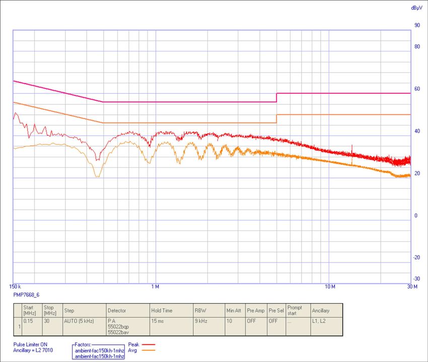
A.6 Conducted Emissions
230 VAC input, 200-mA resistive load connected to PSU with short leads. The conducted emissions in a
pre-compliance test set-up were compared against EN55022 class B limits and found to meet them
comfortably.
SLUA721 – June 2014 AC-DC Non-Isolated SMPS for Single Phase Smart Meters Based on 23
Submit Documentation Feedback UCC28722
Copyright © 2014, Texas Instruments IncorporatedStandby Power and VA www.ti.com
Figure 24. Conducted Emissions as per EN55022 Class B
A.7 Standby Power and VA
The standby power and VA was noted at 240 VAC input with a 2-mA load on 3.3 V and no load on 10 V.
The results were in accordance with the target specifications.
Power consumption = 59 mW
VA = 242 mVA
A.8 Surge Test as per IEC61000-4-5
The 4 kV surge test as per IEC61000-4-5 was performed on the board with no failures.
A.9 EFT Test as per IEC61000-4-4
IEC 61000-4-4 defines the burst immunity test as fast switching disturbance presented in the mains. This
test means the high frequency, high voltage 4 kV, very short pulses (50 ns) are applied between the input
line and neutral. The possible impact seen in the SMPS is unstable operation, that is, restarting of the
SMPS or latching of the SMPS.
The 4-kV burst test was performed on the board with no failures.
24 AC-DC Non-Isolated SMPS for Single Phase Smart Meters Based on SLUA721 – June 2014
UCC28722 Submit Documentation Feedback
Copyright © 2014, Texas Instruments IncorporatedIMPORTANT NOTICE
Texas Instruments Incorporated and its subsidiaries (TI) reserve the right to make corrections, enhancements, improvements and other
changes to its semiconductor products and services per JESD46, latest issue, and to discontinue any product or service per JESD48, latest
issue. Buyers should obtain the latest relevant information before placing orders and should verify that such information is current and
complete. All semiconductor products (also referred to herein as “components”) are sold subject to TI’s terms and conditions of sale
supplied at the time of order acknowledgment.
TI warrants performance of its components to the specifications applicable at the time of sale, in accordance with the warranty in TI’s terms
and conditions of sale of semiconductor products. Testing and other quality control techniques are used to the extent TI deems necessary
to support this warranty. Except where mandated by applicable law, testing of all parameters of each component is not necessarily
performed.
TI assumes no liability for applications assistance or the design of Buyers’ products. Buyers are responsible for their products and
applications using TI components. To minimize the risks associated with Buyers’ products and applications, Buyers should provide
adequate design and operating safeguards.
TI does not warrant or represent that any license, either express or implied, is granted under any patent right, copyright, mask work right, or
other intellectual property right relating to any combination, machine, or process in which TI components or services are used. Information
published by TI regarding third-party products or services does not constitute a license to use such products or services or a warranty or
endorsement thereof. Use of such information may require a license from a third party under the patents or other intellectual property of the
third party, or a license from TI under the patents or other intellectual property of TI.
Reproduction of significant portions of TI information in TI data books or data sheets is permissible only if reproduction is without alteration
and is accompanied by all associated warranties, conditions, limitations, and notices. TI is not responsible or liable for such altered
documentation. Information of third parties may be subject to additional restrictions.
Resale of TI components or services with statements different from or beyond the parameters stated by TI for that component or service
voids all express and any implied warranties for the associated TI component or service and is an unfair and deceptive business practice.
TI is not responsible or liable for any such statements.
Buyer acknowledges and agrees that it is solely responsible for compliance with all legal, regulatory and safety-related requirements
concerning its products, and any use of TI components in its applications, notwithstanding any applications-related information or support
that may be provided by TI. Buyer represents and agrees that it has all the necessary expertise to create and implement safeguards which
anticipate dangerous consequences of failures, monitor failures and their consequences, lessen the likelihood of failures that might cause
harm and take appropriate remedial actions. Buyer will fully indemnify TI and its representatives against any damages arising out of the use
of any TI components in safety-critical applications.
In some cases, TI components may be promoted specifically to facilitate safety-related applications. With such components, TI’s goal is to
help enable customers to design and create their own end-product solutions that meet applicable functional safety standards and
requirements. Nonetheless, such components are subject to these terms.
No TI components are authorized for use in FDA Class III (or similar life-critical medical equipment) unless authorized officers of the parties
have executed a special agreement specifically governing such use.
Only those TI components which TI has specifically designated as military grade or “enhanced plastic” are designed and intended for use in
military/aerospace applications or environments. Buyer acknowledges and agrees that any military or aerospace use of TI components
which have not been so designated is solely at the Buyer's risk, and that Buyer is solely responsible for compliance with all legal and
regulatory requirements in connection with such use.
TI has specifically designated certain components as meeting ISO/TS16949 requirements, mainly for automotive use. In any case of use of
non-designated products, TI will not be responsible for any failure to meet ISO/TS16949.
Products Applications
Audio www.ti.com/audio Automotive and Transportation www.ti.com/automotive
Amplifiers amplifier.ti.com Communications and Telecom www.ti.com/communications
Data Converters dataconverter.ti.com Computers and Peripherals www.ti.com/computers
DLP® Products www.dlp.com Consumer Electronics www.ti.com/consumer-apps
DSP dsp.ti.com Energy and Lighting www.ti.com/energy
Clocks and Timers www.ti.com/clocks Industrial www.ti.com/industrial
Interface interface.ti.com Medical www.ti.com/medical
Logic logic.ti.com Security www.ti.com/security
Power Mgmt power.ti.com Space, Avionics and Defense www.ti.com/space-avionics-defense
Microcontrollers microcontroller.ti.com Video and Imaging www.ti.com/video
RFID www.ti-rfid.com
OMAP Applications Processors www.ti.com/omap TI E2E Community e2e.ti.com
Wireless Connectivity www.ti.com/wirelessconnectivity
Mailing Address: Texas Instruments, Post Office Box 655303, Dallas, Texas 75265
Copyright © 2014, Texas Instruments IncorporatedYou can also read