An electrically switchable wideband metamaterial absorber based on graphene at P band
←
→
Page content transcription
If your browser does not render page correctly, please read the page content below
Open Physics 2021; 19: 460–466
Research Article
Liansheng Wang*, Dongyan Xia, Quanhong Fu, Xueyong Ding, and Yuan Wang
An electrically switchable wideband
metamaterial absorber based on graphene at
P band
https://doi.org/10.1515/phys-2021-0056 storage, microwave engineering, medical imaging, and
received March 15, 2021; accepted July 07, 2021 military technology [1–3]. A metamaterial absorber is a
Abstract: Graphene has the capability of dynamically kind of special structural absorbing material. The basic
tuning its conductivity through gate voltage. Based on design principle of the metamaterial absorber is to achieve
this fact, an electrically switchable wideband meta- a good impedance match with the free space by optimizing
material absorber at low frequencies is presented and the structural unit of the metamaterial. In this state, the
investigated in this paper. Our calculated results show incident electromagnetic wave can be absorbed by the meta-
that its absorption is over 90% from 400 to 1,000 MHz material almost without reflection [4]. Compared with tradi-
with the Fermi level of graphene being at 0 eV and the tional absorbing materials, a metamaterial absorber has the
absorption band can be switched by adjusting the Fermi advantage of simple structure, being controllable, adjus-
level of graphene without changing its physical structure. table, and providing high absorption [5].
Moreover, the surface current distribution enables us to The frequency of electromagnetic waves at the P band
reveal the switchable wideband absorption characteris- is from 0.23 to 1 GHz and is mainly used on long-range
tics of our designed metamaterial absorber. At last, we warning radar [6]. The long wavelength of the electro-
prove that its absorption property is polarization-insensi- magnetic wave at the P band carries great challenges
tive due to the rotational symmetry of the structural unit. on the electromagnetic parameter setting and to control
This work may provide a further step in the development the thickness of the absorbing material. It has great mili-
of switchable sensors and absorbers at low frequencies. tary significance for the study of advanced and efficient
metamaterial absorbers for P-band radar. A metamaterial
Keywords: metamaterial absorber, graphene, switchable, absorber working on the P band can realize electromag-
wideband, low frequency netic stealth of P-band radar. In the aspect of meta-
material absorber research at P band, Liu et al. [7] designed
a circuit resonant metamaterial absorber. The structural
unit of the metamaterial absorber was composed of con-
1 Introduction ductive metal wire loaded with resistors, FR4 dielectric
layer, air layer, and metal plate. The absorption of the
Metamaterials, due to their novel electromagnetic responses optimized structure was more than 90% from 840 to
which are designable and tunable, give us a more effective 960 MHz. Zuo et al. [8] designed a metamaterial absorber
way to control the electromagnetic waves and have exten- with three layers of metal square rings, and the absorp-
sive applications in many areas like optical imaging, optical tion was more than 90% at UHF band (300–3,000 MHz).
Buitung et al. [9] designed an hourglass-shaped meta-
material absorber at P band; its absorption was over
* Corresponding author: Liansheng Wang, Science and Technology 90% at 375 MHz. Nie et al. [10] designed a composite meta-
Department, Sanya University, Sanya 52022, Hainan, China, material absorber by superimposing the resonant meta-
e-mail: wlswls1982@126.com material and the metamaterial was loaded with resistance
Dongyan Xia: Finance and Economics Department, Sanya University, film. The absorption of the designed structure was greater
Sanya 572022, Hainan, China
than 90% from 1 to 7 GHz.
Quanhong Fu: Science Department, Northwestern Polytechnical
University, Xi’an 710072, Shanxi, China
At present, there are few reports on wideband switch-
Xueyong Ding, Yuan Wang: Science and Technology Department, able metamaterial absorber at P band. Based on the tun-
Sanya University, Sanya 52022, Hainan, China able conductivity of graphene, an electrically switchable
Open Access. © 2021 Liansheng Wang et al., published by De Gruyter. This work is licensed under the Creative Commons Attribution 4.0
International License.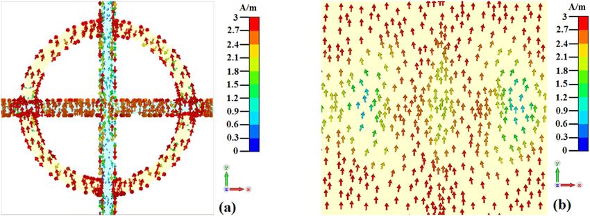
Electrically switchable wideband metamaterial absorber 461
wideband metamaterial absorber at P band is presented
and investigated in this paper. Our calculated results
show that its absorption is over 90% from 400 to
1,000 MHz with the Fermi level of graphene being at 0 eV
and the absorption band can be switched by adjusting the
Fermi level of graphene without changing its physical struc-
ture. Our work may provide a further step in the development
of switchable sensors and absorbers at low frequencies.
2 The tunable conductivity of
graphene
Graphene is a two-dimensional planar crystal that is
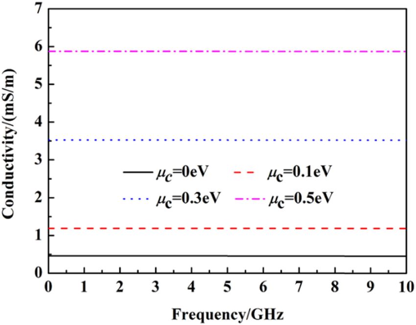
composed of single-layer carbon atoms. Graphene has Figure 1: The conductivity of graphene at different Fermi levels.
very high electron and hole mobility and its conductivity
can be adjusted by changing the bias voltage applied to it 3 Model design
[11]. Therefore, graphene is widely used to design switch-
able metamaterials [12–15]. The surface conductivity of The unit cell of our designed switchable wideband meta-
graphene can be expressed by the Kubo formula from material absorber based on graphene at P band is shown
microwave to visible light band [16] as follows: in Figure 2. The absorber is composed of three layers –
ie 2 (ω − 2i Γ) ⎧ 1 copper ring layer loaded with three thousand layers of
σ (ω , μ C ) = graphene, FR4 dielectric layer (εr = 4.3, tan δ = 0.025),
π ℏ2 ⎨
⎩ ( ω − 2i Γ)2
∞ and copper substrate (σ = 5.96 × 10⁷ S/m). In the simula-
× ∫ε⎡⎣ ∂f∂d ε(ε) −
∂fd ( −ε ) ⎤
∂ε ⎦
dε
(1)
tion process, the three thousand layers of graphene are set
0
as a resistor film with total thickness of 1 μm according to
∞ the calculated conductivity of graphene shown in Figure 2.
⎫
− ∫ (ω −fd (2−iΓε))2 −− f4d ((εε)/ℏ2) dε⎬, In addition, a narrow-band silver electrode is set at the
boundary between the graphene layer and the dielectric
0 ⎭
layer to apply bias voltage. Assuming that the incident
fd (ε ) = [exp(ε − μC ) / kBT + 1]−1 . (2)
In formulas (1) and (2), kB is the Boltzmann constant,
ℏ is the Dirac constant, fd (ε ) is the Fermi-Dirac distribu-
tion, ε is the energy, μC is the Fermi level of graphene, T is
the temperature, and Γ is carrier scattering rate [11].
According to formulas (1) and (2), the relationship of gra-
phene’s conductivity with its Fermi level is shown in
Figure 1 (T = 300 K , Γ = 12.2 meV ) [16].
We can see from Figure 1 that the graphene can be
regarded as a resistor film with tunable conductivity at
microwave band, and its conductivity increases with the
increase of Fermi level [12–15,17]. The relationship of gra-
phene’s Fermi level with the applied bias voltage can be
expressed as [17]:
∞
ε0π ℏ2vF2
e
Ebias = ∫ε[ fd(ε) − fd (ε + 2μC)]dε. (3)
0
Figure 2: The diagram of the switchable wideband metamaterial
In the formula (3), Ebias is the applied bias voltage, absorber based on graphene at P band: (a) perspective view,
vF = 106 m/s is the velocity of electrons [16]. (b) front view, and (c) side view.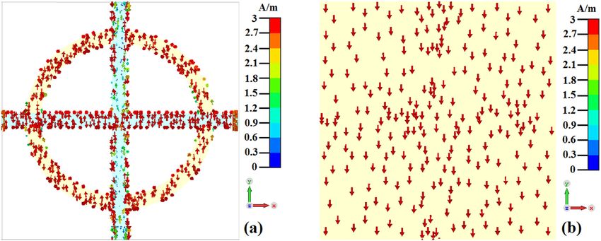
462 Liansheng Wang et al.
microwave is perpendicular to the surface of the meta-
material, the absorption of a metamaterial absorber can
be calculated by the formula A = 1 − ∣S11∣2 − ∣S21∣2 , where
S11 and S21 are the reflection and transmission of metama-
terial absorber, respectively. In order to prevent the break-
down of the dielectric layer by the applied bias voltage, the
Fermi level of graphene is limited to 0–0.5 eV in this work.
The related structure parameters are: a = b = 16 mm, r =
6 mm, c = d = 1 mm, t2 = 0.035 mm, t1 = 1 μm, t3 = 1 mm, t4 =
0.035 mm. The above parameters are the optimized para-
meters obtained during the model designing process based
on the best possible absorption spectra. The commercial soft-
ware CST Microwave studio is used for the full-wave simula-
tion of the designed metamaterial absorber. Throughout
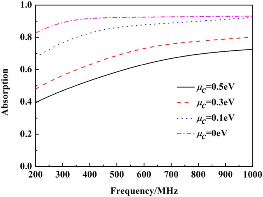
Figure 3: The absorption of metamaterial absorber at different Fermi
the simulation process, the boundary conditions for the x
levels of graphene. and y directions are set as unit cell and the z-direction is
Figure 4: The normalized input impedance of metamaterial absorber with free space: (a) real part and (b) imaginary part.
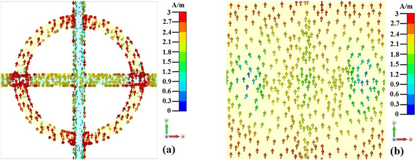
Figure 5: The surface current distribution of metamaterial absorber at 0.5 GHz with the Fermi level of graphene 0 eV: (a) the top metal copper
ring and (b) the metal substrate.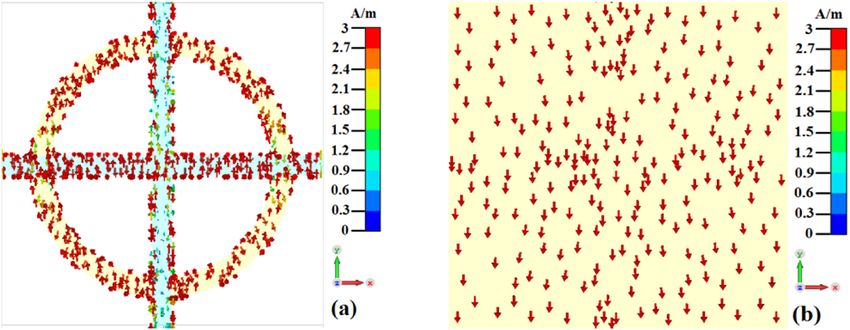
Electrically switchable wideband metamaterial absorber 463
Figure 6: The surface current distribution of metamaterial absorber at 0.8 GHz with the Fermi level of graphene 0 eV: (a) the top metal
copper ring and (b) the metal substrate.
set as open [11]. The All + Floquet ports are used to simulate graphene is 0 eV, and the absorption gradually decreases
the incoming and outgoing waves [11]. The electromagnetic when the Fermi level of graphene increases from 0 to
parameters are calculated by using frequency-domain electro- 0.5 eV, thereby realizing the switchable property of the
magnetic solver [11]. designed wideband metamaterial absorber. According to
the formula of modulation depth M = ∣Abias − Amax ∣ / Amax ,
the maximum modulation depth of the metamaterial
absorber reaches up to 41.7%.
4 Results and discussion The good impedance match between a metamaterial
and the free space is the most important condition to
The calculated absorptions of the metamaterial absorber realize any metamaterial absorber. According to the S11
at different Fermi levels of graphene are shown in Figure 3. and S21 parameters extracted from the simulation, we
We can see from Figure 3 that the absorption is greater calculate the normalized impedance (Z (ω)/ Z0) for the
than 90% from 400 MHz to 1 GHz when the Fermi level of Fermi level of graphene of 0 eV through the scattering
Figure 7: The surface current distribution of metamaterial absorber at 0.5 GHz with the Fermi level of graphene 0.5 eV: (a) the top metal
copper ring and (b) the metal substrate.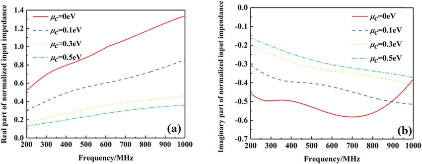
464 Liansheng Wang et al.
Figure 8: The surface current distribution of metamaterial absorber at 0.8 GHz with the Fermi level of graphene 0.5 eV: (a) the top metal
copper ring and (b) the metal substrate.
parameter method [18], as shown in Figure 4. It can be
seen from Figure 4 that the normalized impedance of the
metamaterial absorber with the free space from 400 MHz
to 1 GHz is close to one, which indicates that a well-
acceptable impedance match between the metamaterial
absorber and the free space is accomplished; as an out-
come, the absorption can be realized in this case.
In order to explore the mechanism of wideband
absorption, the surface currents of the absorber at 0.5
and 0.8 GHz with the Fermi level of graphene at 0 eV
are monitored. The results are shown in Figures 5 and 6.
It can be seen from Figures 5(a) and 6(a) that under
the action of electromagnetic wave, the surface currents
of the top copper ring and the metal substrate form an
Figure 9: The absorption of metamaterial absorber at different
antiparallel current, which forms a current loop; this
polarization states with the Fermi level of graphene 0 eV. leads to a strong magnetic response, and then produces
Figure 10: The absorption of metamaterial absorber at different incident angles with the Fermi level of graphene 0 eV: (a) TE mode and (b)
TM mode.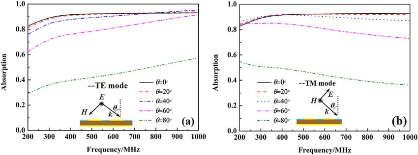
Electrically switchable wideband metamaterial absorber 465
Figures 7 and 8 that it does not produce magnetic reso-
nance and electric resonance under the action of the
incident electromagnetic wave; this leads to the lower
absorption of the metamaterial absorber.
In order to meet the practical applications, a meta-
material absorber needs to have high absorption at different
polarization states and wide-incident angles. Therefore, the
absorption of the metamaterial absorber at different polari-
zation states and different incident angles is calculated (the
Fermi level of graphene is 0 eV); the results are shown in
Figures 9 and 10. It can be seen from Figure 9 that the
absorption property of the metamaterial absorber is polari-
zation-independent. It can be seen from Figure 10 that the
absorber can still maintain high absorption in a wide range
of incident angles at TE mode and TM mode. This is very
Figure 11: The absorption of metamaterial absorber under different
important for practical applications.
structure size parameters c.
Figures 11 and 12 show the absorption of the meta-
material absorber with different structure size parameters
a strong magnetic resonance at the z-direction [19]. At the c and d. It can be seen from Figure 11 that the absorption
same time, the surface currents on the left and right side gradually decreases with the increasing of structure size
of the top copper ring are parallel, which leads to the parameter c. It can be seen from Figure 12 that the absorp-
alternating accumulation of current and the formation tion of the metamaterial absorber under different struc-
of electric dipole resonance. Both magnetic resonance ture size parameters d stays unaltered [11].
and electric resonance are simultaneously realized at
0.5 and 0.8 GHz, respectively, which is the precondition
of forming a metamaterial absorber. The superposition of 5 Summary
different resonant frequencies results in the wideband
absorption of the metamaterial absorber. Metamaterial absorber at P band has great military sig-
In order to explore the mechanism of switchable nificance for P-band radar. An electrically switchable wide-
absorption of the metamaterial absorber, the surface cur- band metamaterial absorber based on graphene at P band is
rents of the absorber at 0.5 and 0.8 GHz are monitored presented in this paper. The absorption of the metamaterial
when the Fermi level of graphene is at 0.5 eV [11]. The absorber is over 90% from 400 to 1,000 MHz with the Fermi
results are shown in Figures 7 and 8. It can be seen from level of graphene 0 eV and the absorption band can be
switched by adjusting the Fermi level of graphene. The
absorber offers the advantages of being based on a simple
structure, providing wideband absorption at low frequen-
cies, and being polarization-independent. It has great appli-
cation value as switchable sensors and absorbers at low
frequency.
Funding information: This work is supported by Hainan
Provincial Natural Science Foundation of China (Granted
number: 620MS062).
Conflict of interest: Authors state no conflict of interest.
Reference
Figure 12: The absorption of metamaterial absorber under different [1] Zhang XC. Terahertz wave imaging: horizons and hurdles. Phys
structure size parameters d. Med Biol. 2002;47(21):3667–77.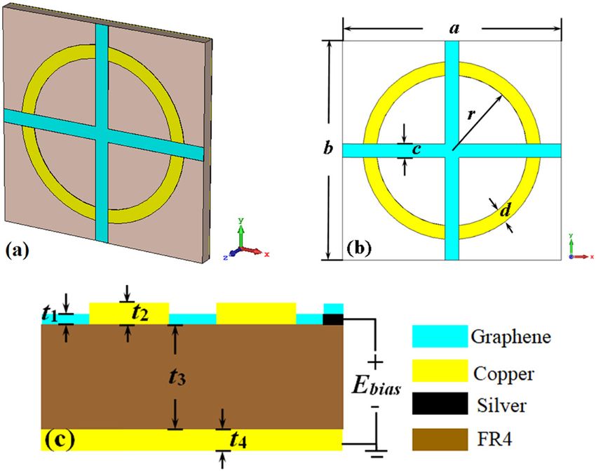
466 Liansheng Wang et al.
[2] Yahiaoui R, Guillet JP, Miollis FD, Mounaix P. Ultra-flexible [11] Wang LS, Xia DY, Fu QH, Ding XY, Wang Y. Graphene-based
multiband terahertz metamaterial absorber for conformal tunable wideband metamaterial absorber with polarization
geometry applications. Opt Lett. 2013;38(23):4988–90. insensitivity and wide incident angle. Front Phys.
[3] Alves F, Grbovic D, Kearney B, Lavrik NV, Karunasiri G. 2020;8:303.
Bi-material terahertz sensors using metamaterial structures. [12] Quader S, Zhang J, Akram MR, Zhu W. Graphene-based high-
Opt Express. 2013;21:13256–70. efficiency broadband tunable linear-to-circular polarization
[4] Gao HT, Wang JJ, Xu BC, Li Z, Liu JW. Research status and converter for Terahertz waves. IEEE J Sel Top Quantum
tendency of sandwich structured metamaterial absorber and Electron. 2020;26(5):4501008–8.
its design optimization. Mater Rep. 2017;31(3):15–20. [13] Zhang J, Wei X, Rukhlenko ID, Chen HT, Zhu W. Electrically
[5] Zhou ZH, Liu XL, Huang DQ, Kang FY. Design and preparation of tunable metasurface with independent frequency and ampli-
a low frequency absorber based on hollowed-out cross- tude modulations. ACS Photonics. 2020;7(1):265–71.
shaped meta-material structure. Acta Phys Sin. [14] Quader S, Akram MR, Xiao F, Zhu W. Graphene based ultra-
2014;63(18):184101. broadband terahertz metamaterial absorber with dual-band
[6] Huo TX, Qiao L, Li FS. High-frequency magnetic properties of tunability. J Opt. 2020;22:095104.
planar anisotropy carbonyl-iron particles. Acta Phys Sin. [15] Akram MR, Ding G, Chen K, Feng Y, Zhu W. Ultrathin single
2014;63(16):167503. layer metasurfaces with ultra‐wideband operation for both
[7] Liu XC, Zhang WW, Hu WX, Jia MQ, He XX, Ben D. High-per- transmission and reflection. Adv Mater. 2020;32:1907308.
formance metamaterial microwave absorber based on 2.5-D [16] Fallahi A, Perruisseau-Carrier J. Design of tunable biperiodic
miniaturization design in UHF band. J Nanjing Univ Aeronau graphene metasurfaces. Phys Rev B. 2012;86:195408.
Astronaut. 2019;51(6):864–9. [17] Wang Y, Wang L, Dong LH, Liu SR, Wang J, Leng YB, et al.
[8] Zuo QY, Yang Y, He XX. Hefei: 2015 National Conference on Design of multifunctional metamaterial absorber based on
Microwave and Millimeter Waves. Beiing of China: Publishing electro-optic properties of graphene. Sci Sin Phys Mech
House of Electronics Industry; 2015. Astron. 2018;48(4):047001.
[9] Buitung S, Khuyenbui V, Dungnguyen V, Yoo YJ, Wonkim K, [18] Smith DR, Schultz S. Determination of effective permittivity
Lamvu D, et al. Small-size metamaterial perfect absorber and permeability of metamaterials from reflection and trans-
operating at low frequency. Adv Nat Sci. 2014;5:045008. mission coefficients. Phys Rev B. 2002;65:195104.
[10] Nie Y, Cheng YZ, Guo RZ. A low-frequency wideband meta- [19] Zou TB, Hu FR, Xiao J, Zhang LH, Liu F, Chen T, et al. Design of a
material absorber based on a cave-disk resonator and resis- polarization-insensitive and broadband terahertz absorber
tive film. Chin Phys B. 2013;22(4):44102. using metamaterials. Acta Phys Sin. 2014;63(17):178103.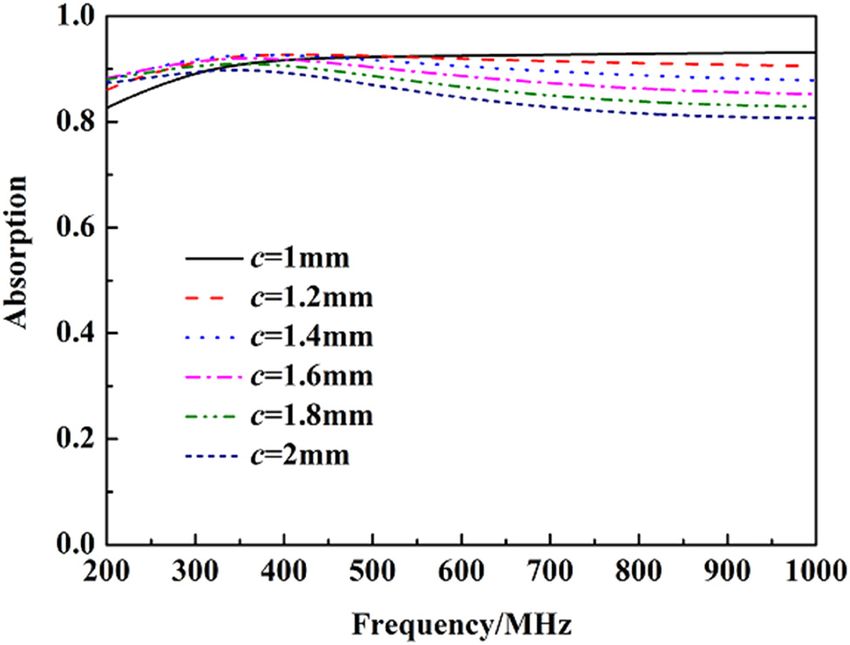
You can also read