An overall summary of my activities as a doctoral student
←
→
Page content transcription
If your browser does not render page correctly, please read the page content below
An overall summary of my activities as a doctoral
                   student

                            Patrick Asenov

                 Institute of Nuclear and Particle Physics
                            NCSR ”Demokritos”

                          October 9, 2020

                                                                                1/75
Patrick Asenov                  PhD Seminar                  October 9, 2020   1 / 75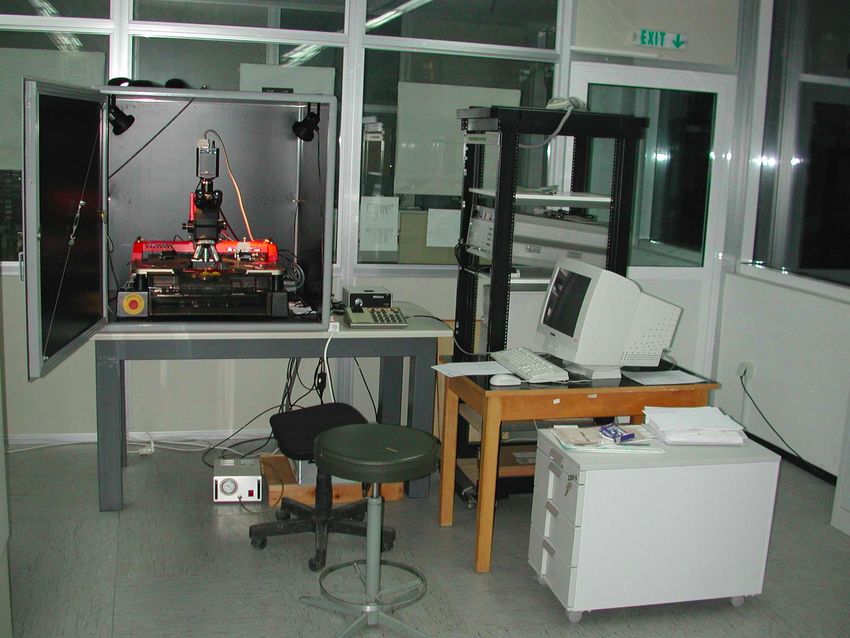
Outline

   The HL-LHC and CMS Phase-2 upgrades
   Silicon sensors
   High-rate particle telescopes

                                                                    2/75
     Patrick Asenov                PhD Seminar   October 9, 2020   2 / 75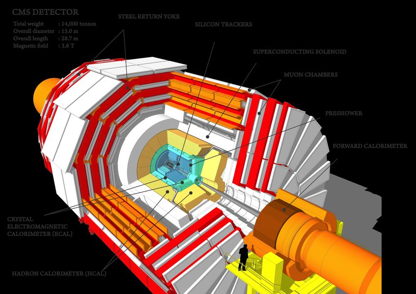
The Large Hadron Collider (LHC)

   The world’s largest and highest-energy
   particle accelerator
   The largest machine in the world
   A 27 km ring of superconducting
   magnets
   Accelerates protons, lead ions
   Two beams traveling in opposite
   directions → collisions
   Record energy of 13 TeV (6.5 TeV per
   beam) for protons; frequency: 40 MHz
   4 large experiments: ALICE, ATLAS,
   CMS, LHCb
                                                                 3/75
     Patrick Asenov             PhD Seminar   October 9, 2020   3 / 75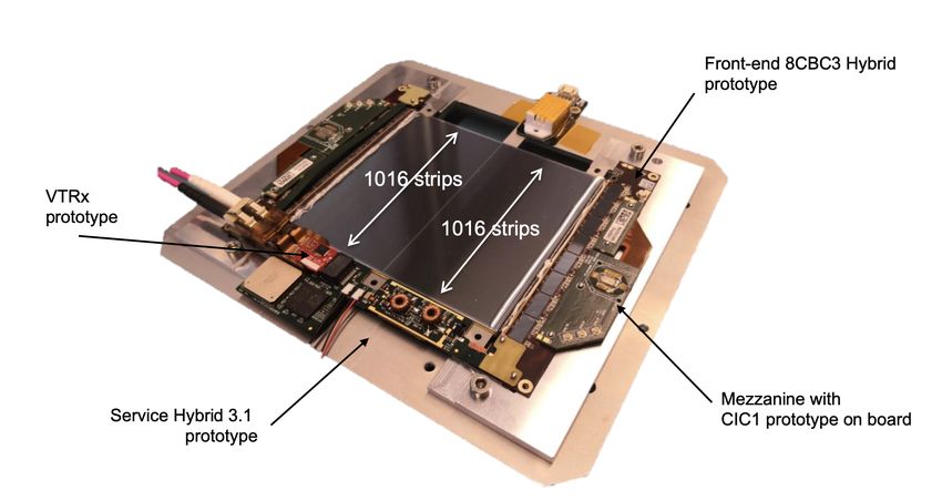
The physics goals of the LHC

   4 July 2012, CMS and ATLAS:
   Higgs boson (∼ 125 GeV)
   8 October 2013, Nobel prize in
   physics: F. Englert and P. Higgs
   Questions unanswered:
         nature of dark matter
         nature of datk energy
         what happened to the
         antimatter after BB
         different mass scale of
         quark/lepton generations
         mechanism through which
         neutrinos obtain their mass
         extra dimensions
         nature and properties of
         quark-gluon plasma                                         4/75
     Patrick Asenov                PhD Seminar   October 9, 2020   4 / 75
The High-Luminosity Upgrade

Objective: to increase the luminosity of LHC by a factor of 10 beyond its
initial design value (peak luminosity: 5 × 1034 cm−2 s−1 , total expected
integrated luminosity: 3000 fb−1 )

                                                                              5/75
      Patrick Asenov             PhD Seminar               October 9, 2020   5 / 75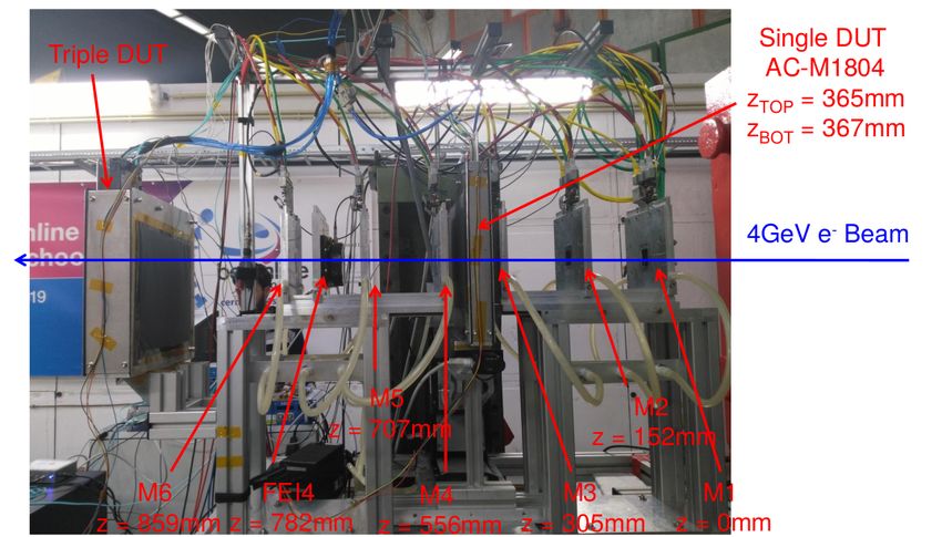
Novel technologies for the HL-LHC

   Cutting-edge 11-12 T superconducting magnets
   Compact superconducting crab cavities with ultra-precise phase
   control for beam rotation
   New technology for beam collimation
   High-power superconducting links with almost zero energy dissipation

                                                                           6/75
     Patrick Asenov            PhD Seminar              October 9, 2020   6 / 75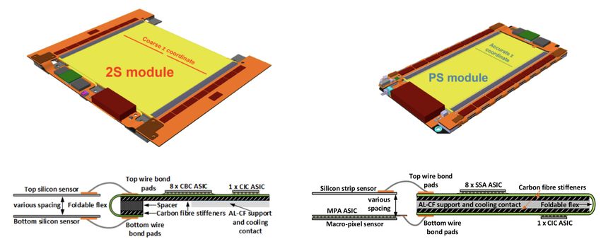
The CMS detector

                                                      7/75
    Patrick Asenov   PhD Seminar   October 9, 2020   7 / 75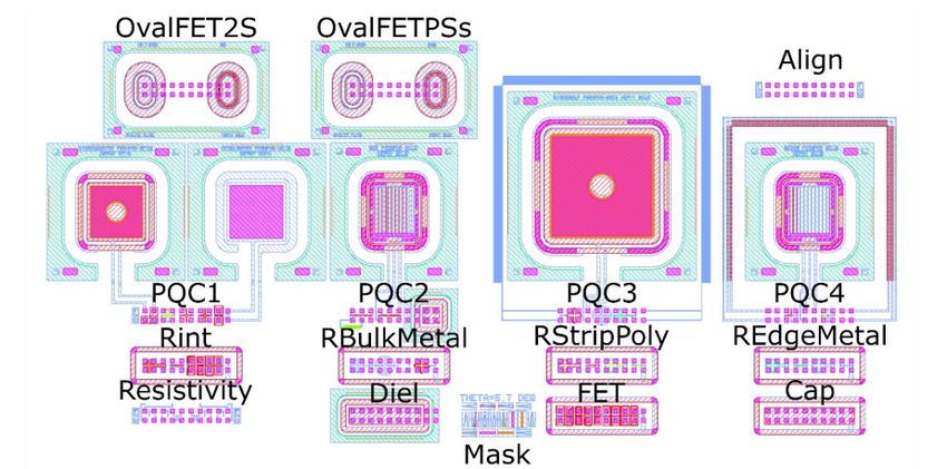
Specific particle interactions in the CMS detector

                                                                  8/75
     Patrick Asenov       PhD Seminar          October 9, 2020   8 / 75
The Phase-2 Upgrade of the CMS Tracker

   Inner Tracker                                Outer Tracker
        unprecedented radiation levels              increased radiation hardness,
        of 1.2 Grad and                             higher granularity and track
        2.3 × 10¹⁶ neq /cm2 and hit                 separation, compatibility with
        rate of 3.2 GHz/cm2                         higher data rates and a longer
        hybrid pixel modules: pixel                 trigger latency
        sensors (pixel size of 2500                 modules with two closely
        µm2 ) and a new 65 nm                       spaced sensors read out by a
        CMOS ASIC (RD53)                            single ASIC which will
        novel scheme of serial                      correlate data from both
        powering                                    sensors to form short track
        high bandwidth readout                      segments (stubs), to be used
        system                                      in tracking at Level-1 trigger
        lightweight mechanics based
        on carbon-fibre material
        two-phase CO2 cooling
                                                                                     9/75
    Patrick Asenov                PhD Seminar                     October 9, 2020   9 / 75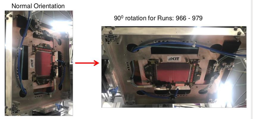
Tracker layout

                                                       10/75
     Patrick Asenov   PhD Seminar   October 9, 2020   10 / 75
The pT module concept
The basic unit of the OT is a pT
module
Endcap Disks and Barrel
region: 2S (outer regions,
above R≈60 cm) and PS
modules (radial range between
R≈20 cm and R≈60 cm)
two closely spaced silicon
sensors (2S: two sensors with
micro-strips; PS one sensor
with micro-strips and one
sensor with macro-pixels)
read out by common
front-end ASICs: correlating
the hits from the two sensors
reject signals with pT smaller
than a given threshold 11/75
Patrick Asenov PhD Seminar October 9, 2020 11 / 75Stubs in the pT module
Front-end ASIC: 1. receives the locations of hits in the transverse plane by
a pT -dependent angle, 2. measures the local distance, 3. compares it to a
predefined acceptance window to select candidates with high pT . A track
stub (a type of a local track segment and matching pair of hits in the two
sensors of a module within a given acceptance window) is formed and
subsequently pushed out to the L1 trigger system at every bunch crossing.
12/75
Patrick Asenov PhD Seminar October 9, 2020 12 / 75Principles of semiconductor devices
Images taken from: Zeghbroeck, Principles of Semiconductor Devices and
Heterojunctions, Prentice Hall; F. Hartmann, Evolution of Silicon Sensor
Technology in Particle Physics, Springer Tracts Mod.Phys. 275 (2017)
13/75
Patrick Asenov PhD Seminar October 9, 2020 13 / 75Particle-matter interaction
Images taken from: M. Tanabashi et al., Review of Particle Physics, Phys.
Rev. D 98, 030001
14/75
Patrick Asenov PhD Seminar October 9, 2020 14 / 75Hamamatsu Photonics K.K. wafers with 2S sensors and
test structures
15/75
Patrick Asenov PhD Seminar October 9, 2020 15 / 75The Tracker quality control process
Vendor Quality Control (VQC), Sensor Quality Control (SQC), Process
Quality Control (PQC), Irradiation Tests (IT)
Structures set for automated PQC
are located on wafers containing
sensors for 2S modules (images from
PQC spec. doc.)
16/75
Patrick Asenov PhD Seminar October 9, 2020 16 / 75The Detector Instrumentation Laboratory (DIL) at NCSR
”Demokritos”
Area of 120 m2 under temperature and humidity control
Meaco 20L Low Energy Dehumidifier
High dry air quality through an Atlas Copco oil-free air compressor
Electrical characterization performed using a Carl Suss PA 150
automatic probe station and supplementary equipment (impedance
analyzer for CV measurements, electrometer/high resistance meter
and SourceMeter for IV measurements, switching matrix and Matrix
Card for switching between IV and CV measurements)
Operation through LabVIEW virtual instruments (VIs)
Environmental simulations with regard to extreme temperature and
humidity performed with a climate test chamber Weiss WKS
3-180/40/5
17/75
Patrick Asenov PhD Seminar October 9, 2020 17 / 75The automatic probe station at DIL
18/75
Patrick Asenov PhD Seminar October 9, 2020 18 / 755 mm sized (full) diodes: IV measurements
2S sensor: ∼ 10 cm × 10 cm
(Active area of a 2S sensor)/(Active area of a full diode) ≈ 400
Left: Measurements of diodes at NCSR ”Demokritos”
Right: Measurements of sensors at UoR
19/75
Patrick Asenov PhD Seminar October 9, 2020 19 / 75MOS capacitors: CV measurements
MOS capacitor: |VFB | must be smaller than 5 V
|VFB | can be evaluated from the CV curve of the MOS capacitor using its
inflection point (a point on a continuous plane curve at which the curve
changes from being concave to convex, or vice versa → where the second
derivative is 0)
20/75
Patrick Asenov PhD Seminar October 9, 2020 20 / 751.25 mm sized (quarter) diode: climate tests
V = −350 V, room temperature, different values of RH
21/75
Patrick Asenov PhD Seminar October 9, 2020 21 / 7560
Irradiation campaign with a Co source
HPK float-zone oxygenated silicon n-in-p test structures (thinned at 240
µm), containing MOS capacitors and diodes, were irradiated at the
secondary standard ionizing radiation laboratory of the Greek Atomic
Energy Commission (GAEC)
22/75
Patrick Asenov PhD Seminar October 9, 2020 22 / 75Equipment for the irradiation campaign
Charged particle equilibrium (CPE) → box of 2 mm-thick Pb and 0.8 mm
of inner lining Al sheet → for the absorption of low energy photons and
secondary electrons (ESCC Basic Specification No. 22900)
Calculated dose rate (in air) at
irradiation point (40 cm from
the source): 0.96 kGy/h using
FC65-P Ionization Chambers
from IBA Dosymetry
Peltier element/thermoelectric
cooler with glue protection to
withstand radiation, fan,
microcontroller for stabilization
of temperature, power supplies
23/75
Patrick Asenov PhD Seminar October 9, 2020 23 / 7560
Co energy spectrum
Taken 4 m away from the cobalt-60
source and after 5.2 cm of Pb (a
5 cm thick Pb block was placed
between the source and the CPE box
and the Pb thickness of the CPE box
was 0.2 cm), as measured inside the
charged particle equilibrium (CPE)
box
Left peak: a backscatter peak at
approximately 200 keV which
emerges when γ-rays enter the
material around the detector and are
scattered back into the detector
Right peaks: corresponding to the
gamma-ray decay modes. 24/75
Patrick Asenov PhD Seminar October 9, 2020 24 / 75Irradiation protocol
Irradiation procedure was split in slots of 6-16 hours of irradiation
During irradiation temperature kept below 20.0 ◦ C
After every irradiation slot:
annealing in the climate test chamber at 60 ◦ C for 10 min
(corresponding to 4 days of annealing at room temperature)
electrical tests after annealing performed using our experimental setup
electrical measurements: 1) Oscillation level = 250 mV; 2) Various
frequencies: 100 Hz, 1 kHz, 10 kHz, 100 kHz, 1 MHz
Between irradiation slots: samples stored in freezer at -28 ◦ C
25/75
Patrick Asenov PhD Seminar October 9, 2020 25 / 75MOS capacitor: CV measurements
Clear evidence of positive charge
induced in the oxide of the MOS
structures after exposure to
γ-photons
Initial shift of the flat band
voltage (VFB ), i.e. the voltage
where the MOS behavior
changes from accumulation to
depletion, to higher absolute
values
26/75
Patrick Asenov PhD Seminar October 9, 2020 26 / 75MOS features from CV (1)
MOS
accumulation
capacitance
variation <
4%
MOS
inversion
capacitance
variation <
10%
Oxide thickness not affected because it is a geometric
characteristic of the device (tox = Coxox ), Cox → from
accumulation region
27/75
Patrick Asenov PhD Seminar October 9, 2020 27 / 75MOS features from CV (2)
Flatband
capacitance
increases after
initial irradiation
but remains
almost stable
afterwards
CFB = 1 1 LD
Cox
+ s
where LD is the
Debye length
28/75
Patrick Asenov PhD Seminar October 9, 2020 28 / 752.5 mm sized (half) diode: IV measurements
Scaling to 20 ◦ C:
gE 1 1
293 K 2 − 2kB ( 293 K − T )
I (20 ◦ C ) = I (T )
T e , Eg = 1.21 eV (RD50 TN
2011-01)
29/75
Patrick Asenov PhD Seminar October 9, 2020 29 / 75Annealing
Time lapses between two consecutive irradiation slots: ∼ 11 h - 15 h →
the samples were stored at −28 ◦ C
When measuring the IV after each
period of storage in the freezer, Annealing process was also observed
annealing was observed every time after storage of the samples in a
bottle of liquid N2
30/75
Patrick Asenov PhD Seminar October 9, 2020 30 / 75Summary of the irradiation campaign
Irradiation using 60 Co source of 11 TBq
Total dose ∼86 kGy
Irradiation of the MOS capacitor shows significant change in the
flatband voltage, threshold voltage and depletion region slope (related
to the charge concentration
Diode CV measurements showed stable depletion voltage with dose as
expected for oxygenated structures
Diode IV measurements showed no breakdown behavior
Annealing phenomena observed when using freezer at −28 ◦ C to store
sample between irradiation slots
Phenomenon persisting also at −196 ◦ C (liquid N2 )
31/75
Patrick Asenov PhD Seminar October 9, 2020 31 / 75The need for high-rate telescopes
Extensive beam tests of the 2S modules are necessary (for channel
efficiency, cluster size, cross talk between adjacent channels etc.)
Existing telescopes used by CMS use a Monolithic Active Pixel Sensor
chip with an integration time of 115.2 µs or 8.68 kHz readout
frequency; integration time in Phase-2 Tracker modules (and other
HL-LHC sensors) is 25 ns → 40 MHz (× 4600 the today’s CMS
telescopes readout frequency)
We cannot test Phase-2 modules at nominal rates with the old
telescopes used by CMS →; that’s why new high-rate telescopes are
being developed, e.g. CHROMIE at CERN and CHROMini at
IPHC-Strasbourg
For CHROMIE see P. Asenov, Commissioning and simulation of
CHROMIE, a high-rate test beam telescope, JINST 15 (2020) 02,
C02003 and my dissertation
32/75
Patrick Asenov PhD Seminar October 9, 2020 32 / 75Description of the telescopes
CHROMIE: particle rates up to 200 MHz/cm2 (the highest rate of a
Phase-2 Outer Tracker DUT: 50 MHz/cm2 ); resolution of the order
of 10-20 µm; pixel size: 100 × 150 µm2 ; 8 layers, each containing
two CMS Phase-1 BPIX modules (Grade C, active area of 2 × 16.2 ×
64.8 mm2 ) in a frame, 4 layers in front of the DUT, and 4 layers
behind it; 20◦ tilt angle about x-axis; 30◦ skew angle about y -axis for
all layers → to allow charge sharing between pixels; a block mounted
on a carriage that can slide over rails holds each layer; auxiliary
electronics mounted close to the modules, on the rails; 4 scintillators
for triggering mounted on the rails; two in front of the layers, two
behind it; actuators for DUT, translation in X/Y, rotation about X;
CMS-standard readout system → SPS, 120 GeV π+ , 40 MHz
CHROMini: very similar, but with only two planes and without any
rotations of the planes → CYRCé, 25 MeV protons, 85 MHz time
structure (can be made half with a kicker)
33/75
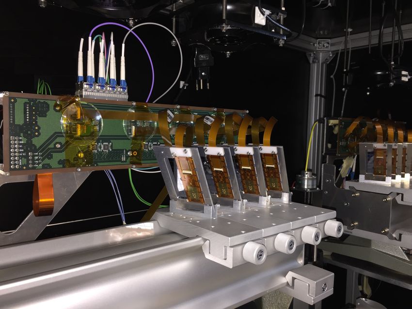
Patrick Asenov PhD Seminar October 9, 2020 33 / 75Visualization of the high-rate telescopes
The CHROMini telescope (top:
The CMS High Rate telescOpe photo from IPHC)
MachInE (CHROMIE)
34/75
Patrick Asenov PhD Seminar October 9, 2020 34 / 75Activities related to telescopes
Pre-calibration of Phase-1 BPIX
modules for CHROMIE with
pXar
Development of a standalone
Geant4 simulation program for
the operation of CHROMIE and
CHROMini under beam
Tracking/alignment algorithm
for CHROMIE (CMSSW
CalDel (delay of the pulse) versus
framework)
VThrComp (global ROC threshold)
Comparison between test beam → ”Tornado plot”
data and simulation output
35/75
Patrick Asenov PhD Seminar October 9, 2020 35 / 75The Geant4 standalone simulation programs
Useful tools for the prediction of a pixel telescope behavior under
beam
In the case of CHROMIE → to give an indication of unknown beam
parameters through comparison of its output with plots from real
data where some magnitudes were unknown (e.g. beam size)
In the case of CHROMini → during the design phase:
to show that the CHROMini project is feasible and can be used for
tracking
to determine the optimal materials, thicknesses and pixel sizes, for
various distances from the DUT, through different simulation runs
to estimate the DUT and telescope module residuals, as well as the
angular straggling (for multiple scattering)
These simulation programs could work as a potential basis for the
study of pixel telescopes or experiments with similar strip/pixel
modules
36/75
Patrick Asenov PhD Seminar October 9, 2020 36 / 75Simulation characteristics for CHROMini (1)
2S module DUT: 2 Si sensors (102700 µm × 94108 µm × 320 µm),
with spacing between the sensors: ∼ 2 mm; strip pitch: 90 µm;
active depth: 290 µm
2 pixel layer consisting of two Phase-1 BPIX modules each, one in
front and one behind the DUT; BPIX module: 66.6 mm × 25 mm ×
460 µm, 2 rows × 8 ROCs; pixel size: 150 µm × 100 µm
A 50 µm thick Al foil at the beam line exit to separate the vacuum
from the air
A PVT (C9 H10 ) scintillator of 2 mm thickness in front of the DUT
and one similar scintillator behind the pixel layer, for triggering
25 MeV proton beam in z-direction
Two scintillators, one before the first pixel ayer (along the way of the
beam) and one behind the second pixel layer, used for triggering
37/75
Patrick Asenov PhD Seminar October 9, 2020 37 / 75Simulation characteristics for CHROMini (2)
z0 = −23.5 cm (the World boundary) → the z-positions of the
centroids of each physical volume are: z0 + 7.6 cm for the first
scintillator, z0 + 11.7 cm for the first pixel layer, z0 + 13.5 cm for the
2S DUT, z0 + 15.3 cm for the second pixel layer and z0 + 16.7 cm for
the second scintillator
20000 events for all plots presented below, except where mentioned
otherwise
Similar plots have been produced for CHROMIE
38/75
Patrick Asenov PhD Seminar October 9, 2020 38 / 75Physics processes
Ionization
Bremsstrahlung
Pair production
Annihilation
Photoelectric effect
γ-production
Compton scattering
Rayleigh scattering
Klein-Nishina model for the differential cross section
General Particle Source (GPS) used instead of a particle gun (since it
allows the specifications of the spectral, spatial and angular distribution of
the primary source particles): position adjusted to the center of the beam
from the data of a real run; only one pixel module hit
Circular beam: σr = 2.123 mm 39/75
Patrick Asenov PhD Seminar October 9, 2020 39 / 75Energy deposition per pixel/strip
40/75
Patrick Asenov PhD Seminar October 9, 2020 40 / 75Detector resolution
Determination of impact points:
Npixels Nstrips
1 X 1 X
Rpixel = wpi Ppi Rstrip = ws Psi (1)
Npixels Nstrips
i=1 i=1
where Npixels is the total number of pixels that have counted a hit in the
current module, the weight
charge collected in the i−th pixel with a hit
wpi = total charge collected in all hit pixels in the current module and Ppi the
geometrical center of the front surface (along the way of the beam) of the
i-th pixel that has counted a hit in the current event; Nstrips is the total
number of strips that have counted a hit in the current sensor, the weight
ws = number of hit strips1in the current sensor and Psi the geometrical center of
the front surface (along the way of the beam) of the i-th strip that has
counted a hit
41/75
Patrick Asenov PhD Seminar October 9, 2020 41 / 75Detector residuals: Calculation
Calculation of residuals:
~rAD = ~rD − ~rA = (xAD , yAD , zAD ) (2)
x − xA y − yA z − zA
= = (3)
xAD yAD zAD
zB 0 = zB , zC 0 = zC (4)
zB − zA zC − zA
xB 0 = xAD + xA , xC 0 = xAD + xA (5)
zAD zAD
zB − zA zC − zA
yB 0 = yAD + yA , yC 0 = yAD + yA (6)
zAD zAD
s1x = xB − xB 0 , s1y = yB − yB 0 , s2x = xC − xC 0 , s2y = yC − yC 0 (7)
42/75
Patrick Asenov PhD Seminar October 9, 2020 42 / 75Residuals and deflection angle
Deflection angle:
uA · u~D )
θd = arccos (~
Y-residuals for the first 2S sensor
0
(B By ) and the second 2S sensor
0
(C Cy ) along the way of the beam 43/75
Patrick Asenov PhD Seminar October 9, 2020 43 / 75Energy deposited in the various volumes of the geometry
44/75
Patrick Asenov PhD Seminar October 9, 2020 44 / 75Kinetic energy of a primary proton vs. z for a single event
45/75
Patrick Asenov PhD Seminar October 9, 2020 45 / 75Other output of the simulation
Total energy lost by the primary
protons in the 2S sensors
Projected hit maps along columns
and along rows for the hit module of
the 2nd pixel layer along the way of
the beam 46/75
Patrick Asenov PhD Seminar October 9, 2020 46 / 75Hit map: comparison with test beam data from IPHC
Hit occupancy per column per row for the hit module of the second pixel
layer; the module is operated at a depletion voltage of −100 V
47/75
Patrick Asenov PhD Seminar October 9, 2020 47 / 75CHROMIE: hit positions (Layer 2)
Hit positions per column per row for the left module of Layer 2 for a
120 GeV π+ beam (beam diameter = 15 mm and σE = 100 keV)
48/75
Patrick Asenov PhD Seminar October 9, 2020 48 / 75Test beam characterization of a 2S module
TB21, DESY, October-November 2019; 4 GeV electrons; 2S modules
as DUT produced at KIT, RWTH-Aachen, Brown University
DATURA telescope
EUDET-type
6 pixel detector planes equipped with MIMOSA 26
pixels sized 18.4 µm × 18.4 µm, arranged in 1152 columns and 576
rows
sensors thinned down to a thickness of about 50 µm and together with
50 µm of thin protective lightproof Kapton foil (25 µm on each side of
a sensor)
Goals: verification of the uniformity of efficiencies; check for
inefficiencies or hit/stub duplications in the center of a 2S; check stub
finding inefficiency for tracks inclined along the strips; measurement
of efficiency and noise hit rate versus the threshold...
49/75
Patrick Asenov PhD Seminar October 9, 2020 49 / 75The initial configuration
50/75
Patrick Asenov PhD Seminar October 9, 2020 50 / 75Data analysis
Data analysis performed either within the scope2s framework (developed
mostly by DESY members) or within the EUTelescope framework
(developed mostly by KIT members)
Goal of our group: to calculate the stub efficiency for various
configurations
Event selection:
1 Reconstruct clusters in the six DATURA planes
2 Fit a track with the fist three DATURA planes
3 Fit a track with all the six DATURA planes
4 If a track that fulfills the above conditions is found then:
1 Reconstruct cluster in both DUT planes
2 Declare a cluster-track match if |∆xcluster−track | < 0.1 mm
3 Check if a stub exists, and if it does declare a stub-track match if
|∆xstub−track | < 0.2 mm
51/75
Patrick Asenov PhD Seminar October 9, 2020 51 / 75Stub efficiency for an angular scan (scope2s)
After the end of each run, the number of cluster-track matches Q1 and the
number of stub-track matches Q2 are printed out → the stub efficiency is
defined as Q2 /Q1
scope2s used for the analysis
Rotations about the y -axis pT [GeV ] = 0.57 · R[m]
sin(α) , R = 0.6 m
Vbias = −300V
Fit performed using a generic FCN
function 52/75
Patrick Asenov PhD Seminar October 9, 2020 52 / 75Tracks inclined along the strips (scope2s)
Before, the length of the strips was
along the y -axis (vertical axis), here
it was along the x-axis (horizontal
axis)
Steady x = 114.662 mm and
y = 47.278 mm and rotations about
the y -axis
53/75
Patrick Asenov PhD Seminar October 9, 2020 53 / 75Summary
Irradiation campaign with 60 Co γ-photons and subsequent electrical
characterization showed that a few hours of annealing are enough to
decrease the leakage current of the sensors; leakage current of the
order of 100 nA even after ∼ 90 kGy of irradiation; proven suitability
of the devices for high-luminosity applications
Standalone simulation programs for pixel telescope operation under
various types of beam → can be used for the design of future pixel
telescopes or tracker systems
Stub efficiency of a 2S module determined for a classic angular scan
and an angular scan along the strips
54/75
Patrick Asenov PhD Seminar October 9, 2020 54 / 75References (1)
P. Asenov, Commissioning and simulation of CHROMIE, a high-rate test
beam telescope, JINST 15 (2020) 02, C02003.
P. Asenov, P. Assiouras et al., Cobalt-60 gamma irradiation of silicon test
structures for high-luminosity collider experiments, PoS Vertex2019 (2020)
061.
P. Assiouras, P. Asenov et al., A program for fast calculation of
capacitances, in planar pixel and strip silicon sensors, PoS Vertex2019
(2020) 059.
CMS collaboration, The phase-2 upgrade of the CMS tracker, CERN,
Geneva, Switzerland, Rep. CERN-LHCC-2017-009.
W Adam et al., P-type silicon strip sensors for the new CMS Tracker at
HL-LHC, JINST 12 (2017) 06, P06018.
W Adam et al., Characterisation of irradiated thin silicon sensors for the
CMS phase II pixel upgrade, Eur.Phys.J.C 77 (2017) 8, 567.
55/75
Patrick Asenov PhD Seminar October 9, 2020 55 / 75References (2)
W Adam et al., Beam test performance of prototype silicon detectors for
the Outer Tracker for the Phase-2 Upgrade of CMS, JINST 15 (2020) 03,
P03014.
P. Asenov, Test beam facility at CYRCé for high particle rate studies with
a CMS upgrade module: design and simulation, 7th Beam Telescopes and
Test Beams Workshop, 14-18 January 2019, CERN.
P. Asenov, Contribution of INPP to the CMS Phase-2 Upgrade, HEP 2019
- Conference on Recent Developments in High Energy Physics and
Cosmology 17-20 April 2019, NCSR ”DEMOKRITOS”, Athens, Greece.
P. Asenov, Performance of a simple 2-plane telescope (CHROMini) and a
CMS 2S module in a 25 MeV proton beam: Comparison between data and
Geant4 simulation, 8th Beam Telescopes and Test Beams Workshop,
27-31 January 2020, Tbilisi State University.
56/75
Patrick Asenov PhD Seminar October 9, 2020 56 / 75Backup
57/75
Patrick Asenov PhD Seminar October 9, 2020 57 / 75Properties of silicon
1
f (E ) = E −EF (8)
e kB T
+1
EC −EF
−
n = NC e kB T
(9)
EF −EV
−
p = N V e kB T (10)
3
2πme∗ kB T 2
NC = 2 (11)
h2
3
2πmh∗ kB T 2
NV = 2 (12)
h2
√ p E
− G
ni = np = n = p = NC NV e 2kB T (13)
58/75
Patrick Asenov PhD Seminar October 9, 2020 58 / 75p-n diode (1)
Jp = Jp, Drift + Jp, Diffusion = qµp pE − qDp ∇p (14)
Jn = Jn, Drift + Jn, Diffusion = qµn nE + qDn ∇n (15)
J = Jp + Jn (16)
ND N A
Vbi = VT ln (17)
ni
V = Va − Vbi (18)
xd = xn + xp (19)
Qn = qND xn (20)
Qp = −qNA xp (21)
59/75
Patrick Asenov PhD Seminar October 9, 2020 59 / 75p-n diode (2)
s
2s 1 1
xd = + (Vbi − Va ) (22)
q NA ND
s
2s NA 1
xn = (Vbi − Va ) (23)
q N D NA + N D
s
2s ND 1
xp = (Vbi − Va ) (24)
q NA NA + N D
r
qs NA ND s
Cj = , Cj = (25)
2(Vbi − Va ) NA + ND xd
1
ρ= (26)
q(nµn + pµp )
60/75
Patrick Asenov PhD Seminar October 9, 2020 60 / 75MOS capacitor
Z tox
Qi 1
VFB = ΦMS − − ρox (z)zdz (27)
Cox ox 0
Qd = −qNA xd (28)
qNA xd
Es = (29)
s
√
4s qNA φF
VT = VFB + 2φF + (30)
Cox
1
CFB = 1 LD
(31)
Cox + s
s
s VT
LD = (32)
qNA
61/75
Patrick Asenov PhD Seminar October 9, 2020 61 / 75Particle-matter interaction
2me c 2 β 2 γ 2 Wmax
dE 2Z
1 1 2 δ(βγ)
− = Kz ln −β − (33)
dx A β2 2 I2 2
2me c 2 β 2 γ 2
Wmax = (34)
me 2
1 + 2γ m
M +
e
M
∆Ivol
= αΦ (35)
V
62/75
Patrick Asenov PhD Seminar October 9, 2020 62 / 75Silicon sensors as particle detectors
i = qvEv (36)
q
ENC = ENCC2d + ENCI2L + ENCR2P + ENCR2S (37)
2mc 2 β 2 γ 2
ξ 2
∆p = ξ ln + ln + j − β − δ(βγ) (38)
I I
where ξ = (K /2) hZ /Ai z 2 (x/β 2 ) and j = 0.2
p
x=√ (39)
12
63/75
Patrick Asenov PhD Seminar October 9, 2020 63 / 75VFB - Noxide relation
VFB can be expressed as a sum of: the difference between work functions
of metal and semiconductor (which remains stable), the voltage across the
oxide due to the charge at the oxide-semiconductor interface and a third
term which is due to Noxide
64/75
Patrick Asenov PhD Seminar October 9, 2020 64 / 752.5 mm sized (half) diode: CV measurements
Gunnar Lindström, Radiation
Damage in Silicon Detectors, Nucl.
Instr. and Meth. A.
65/75
Patrick Asenov PhD Seminar October 9, 2020 65 / 75The Phase-1 BPIX sensor geometry
66/75
Patrick Asenov PhD Seminar October 9, 2020 66 / 75CHROMIE: Tracking
Tracking strategy:
Removing noisy channels
Applying a coarse alignment (demanding that all tracks should be
parallel to the beam axis)
Seeding
Pattern recognition
Seeding: a search (conducted using global coordinates) for 2 points,
one in Seeding Layer 1 and one in Seeding Layer 2, with ∆x < 0.1 cm
and ∆y < 0.1 cm (corrected for misalignment: translation on x-axis +
50 cm → a new (0, 0, 0) point); loop on the clusters of the seeding
modules
First check L1-L2, then L2-L3, then L3-L4, until a seed is found. (The
layers on the arm of CHROMIE behind the DUT, on the way of the
beam, weren’t used because two dead and one noisy modules are
located there.)
67/75
Patrick Asenov PhD Seminar October 9, 2020 67 / 75CHROMIE: analysis results
Pattern recognition: look for the cluster with the smallest 2D distance
from the track within the telescope layer → fit the track including the
new cluster in the list, minimizing the 2D distance in the telescope
layer
Short tracks (that not hit at least 4 modules) are not considered valid
tracks
Seeding efficiency: 78.7%. Note: In our run analysis:
(Number of events with at least 4 layers with at least one cluster and 0
seeds)/(Number of events with at least 4 layers with at least one
cluster) = 6082/28551 = 21.3%
Number of events with 0 layers with at least 1 cluster = 1015 →
1015/32536 = 3.12% of the total events → upper limit for efficiency is
96.88%
68/75
Patrick Asenov PhD Seminar October 9, 2020 68 / 75CHROMIE residuals (Layer 3)
69/75
Patrick Asenov PhD Seminar October 9, 2020 69 / 75CHROMIE: cluster size
70/75
Patrick Asenov PhD Seminar October 9, 2020 70 / 75CHROMini: kinetic energy of a primary proton vs. z
71/75
Patrick Asenov PhD Seminar October 9, 2020 71 / 75Basic difference between EUTelescope and scope2s
frameworks regarding the stub efficiency
EUTelescope compares a track directly to the stub, without any
selection based on the hits, and thus examines the efficiency of the
full 2S module to produce a stub for a given incident track
scope2s uses only tracks that are matched to hits in each of the
sensors of the 2S module, and thus checks that the CBC stub
correlation logic is working as expected
When the DUT is rotated, the displacement between the hits in the two
sensors of the 2S module becomes larger, and at a certain angle the
number of stubs is expected to decrease → in case that a hit is lost by one
of the sensors and no stub is created, in the EUTelescope approach this
would be counted as an inefficient event, while in the scope2s approach it
would not be counted at all and the event wouldn’t be included in the
analysis
72/75
Patrick Asenov PhD Seminar October 9, 2020 72 / 75DATURA alignment
Each sensor plane defines a local coordinate systems for its hits (columns
and rows for pixels; rows for strips). The second telescope plane defines
the global xy reference system. The beam is along the z-axis, and the
tracks of the primary particles are straight since there is no magnetic field
present in the telescope system. The alignment is hierarchical: the 1st and
3rd telescope planes are aligned relatively to the 2nd (x- and y -shifts and
rotation), the 4th and 6th telescope planes are aligned relatively to the 5th
(x- and y -shifts and rotation), and the downstream triplet is aligned
relatively to the upstream triplet (x, y - and z-shifts). While for the
telescope alignment the coordinates of the hits are changed (active
transformations), for the DUT the coordinates of the reference frame are
changed instead (passive transformations) and all corrections are applied
only to the track. The intersection of the telescope tracks with the tilted
DUT is calculated and transformed into DUT coordinates to allow detailed
DUT studies.
73/75
Patrick Asenov PhD Seminar October 9, 2020 73 / 752S module alignment
The alignment of the DUT itself is primarily based on profile plots and
projections and for its implementation it is assumed that the 2S sensors
are planar. The alignment consists of a set of shifts of axes, rotations
around the beam axis and adjustments of the tilt angle and the skew
angle. The method converges after a few iterations.
74/75
Patrick Asenov PhD Seminar October 9, 2020 74 / 75Tracks inclined along the strips (EUTelescope)
Before, the length of the strips was
along the y -axis (vertical axis), here
it was along the x-axis (horizontal
axis)
Steady x = 114.662 mm and
y = 47.278 mm and rotations about
the y -axis
75/75
Patrick Asenov PhD Seminar October 9, 2020 75 / 75You can also read