Charge-Density-Wave-Induced Peak-Dip-Hump Structure and Flat Band in the Kagome
←
→
Page content transcription
If your browser does not render page correctly, please read the page content below
Charge-Density-Wave-Induced Peak-Dip-Hump Structure and Flat Band in the Kagome
                                                                                       Superconductor CsV3 Sb5

                                                                  Rui Lou,1, 2, 3, ∗ Alexander Fedorov,2, 3, † Qiangwei Yin,4 Andrii Kuibarov,2 Zhijun Tu,4 Chunsheng
                                                                      Gong,4 Eike F. Schwier,5, 6 Bernd Büchner,2, 7 Hechang Lei,4, ‡ and Sergey Borisenko2, §
                                                                               1
                                                                                 School of Physical Science and Technology, Lanzhou University, Lanzhou 730000, China
                                                                       2
                                                                           Leibniz Institute for Solid State and Materials Research, IFW Dresden, 01069 Dresden, Germany
                                                                                                   3
                                                                                                     Helmholtz-Zentrum Berlin für Materialien und Energie,
                                                                                                   Elektronenspeicherring BESSY II, 12489 Berlin, Germany
                                                                                     4
                                                                                       Department of Physics and Beijing Key Laboratory of Opto-electronic Functional
                                                                                  Materials & Micro-nano Devices, Renmin University of China, Beijing 100872, China
arXiv:2106.06497v2 [cond-mat.supr-con] 2 Jul 2021

                                                                             5
                                                                               Experimentelle Physik VII, Universität Würzburg, Am Hubland, 97074 Würzburg, Germany
                                                                                                 6
                                                                                                   Würzburg-Dresden Cluster of Excellence ct.qmat, Germany
                                                                                 7
                                                                                   Institute for Solid State and Materials Physics, TU Dresden, 01062 Dresden, Germany
                                                                     The entanglement of charge density wave (CDW), superconductivity, and topologically nontrivial electronic
                                                                  structure has recently been discovered in the kagome metal AV3 Sb5 (A = K, Rb, Cs) family. With high-resolution
                                                                  angle-resolved photoemission spectroscopy, we study the electronic properties of CsV3 Sb5 deep in the CDW
                                                                  state. The spectra around K̄ is found to exhibit a peak-dip-hump structure associated with two separate branches
                                                                  of dispersion, demonstrating the isotropic CDW gap opening. The peak-dip-hump lineshape is contributed by
                                                                  linearly dispersive Dirac bands in the lower branch and a dispersionless flat band close to EF in the upper branch.
                                                                  The Fermi surface nesting scenario can account for these CDW-related features. The high density of states at
                                                                  EF associated with the flat band could play an essential role in the onset of superconductivity.

                                                       Recently, exploring the mutual interactions of different cor-          the softening of acoustic phonon is absent near the CDW vec-
                                                    related states, magnetism, and non-trivial band topology be-              tor [33], and no CDW amplitude mode is identified in an ul-
                                                    came of great scientific interest, where novel quantum phe-               trafast pump-probe reflectivity experiment [44], pointing to
                                                    nomena such as quantum anomalous Hall effect [1–3], topo-                 an unconventional mechanism. Another STM measurement
                                                    logical superconductivity [4–8], pair density wave [9, 10],               further suggests the presence of topological 2 × 2 CDW in
                                                    and topological Chern magnetism [11, 12] have been inten-                 KV3 Sb5 [25], which energetically favors a chiral flux phase
                                                    sively studied both in experiment and theory. A peak-dip-                 [45, 46] and may explain the observed large anomalous Hall
                                                    hump lineshape induced by symmetry breaking or bosonic                    effect [22, 26].
                                                    mode coupling with the fermionic quasiparticle usually arises                Several angle-resolved photoemission spectroscopy
                                                    in the single-particle spectrum of the correlated electron sys-           (ARPES) studies have been carried out to understand the
                                                    tems such as actinides [13], cuprates [14, 15], iron chalco-              fascinating CDW state [47–50]. Temperature-induced band
                                                    genides [16], and colossal magnetoresistive manganites [17,               renormalizations and van Hove singularities have been
                                                    18]. Comprehensive knowledge of the renormalized elec-                    observed in RbV3 Sb5 and CsV3 Sb5 [50–52]. Meanwhile,
                                                    tronic states and the redistribution of spectral weight inside            many efforts have been devoted to resolving the CDW
                                                    the peak-dip-hump structure is essential for uncovering the               gap in CsV3 Sb5 . Nevertheless, two helium-lamp-based
                                                    microscopic mechanism of the intertwined correlated phases.               measurements report strong anisotropy of CDW gap opening
                                                                                                                              around K̄ [47, 48], in sharp contrast to the nearly isotropic
                                                       The kagome lattice, composed of two-dimensional (2D)
                                                                                                                              gap behavior around K̄ from another synchrotron-based study
                                                    network of corner-sharing triangles, is characterized by the
                                                                                                                              [49]. In order to clarify the discrepancy and gain insight
                                                    coexistence of topologically protected Dirac bands and non-
                                                                                                                              into the underlying scenario of CDW order, further ARPES
                                                    dispersing or flat bands, offering a fertile playground to study
                                                                                                                              measurements are desired.
                                                    the interplay of electron correlations and non-trivial band
                                                    topology [19]. Recently, the vanadium-based kagome metal                     In this work, we perform a high-resolution ARPES study
                                                    AV3 Sb5 (A = K, Rb, Cs) family with a non-zero Z2 topolog-                on CsV3 Sb5 . Deep in the CDW phase, we reveal a peak-dip-
                                                    ical invariant has been discovered to host both charge den-               hump feature around K̄ contributed by two separate branches
                                                    sity wave (CDW) and superconductivity, arousing numerous                  of dispersion, showing the isotropic CDW gap opening. Lin-
                                                    interests in the community [20–42]. Scanning tunneling mi-                early dispersive Dirac bands characterize the hump structure
                                                    croscopy (STM) [32] and x-ray scattering measurements [33]                at higher binding energy, and the peak structure exhibits a flat
                                                    have demonstrated a three-dimensional (3D) charge modula-                 band close to EF . The origin of these features can be well ex-
                                                    tion with a 2 × 2 × 2 superstructure, which associates with               plained by the FS nesting scenario. The high density of states
                                                    the CDW formation at 80–110 K [20, 21, 23, 24, 39]. Inter-                (DOS) at EF associated with the flat band could promote the
                                                    estingly, an optical spectroscopy study suggests the CDW is               onset of superconductivity.
                                                    driven by the Peierls instability related to Fermi surface (FS)              High-quality single crystals of CsV3 Sb5 were grown by the
                                                    nesting [36], in favor of the theoretical calculations [43], but          self-flux method [39]. Detailed experimental methods can be
2
intensity plots and corresponding second derivative plots are
shown in Fig. 2. The overall band structure agrees with previ-
ous ARPES studies [49, 50] and theoretical calculations [43].
As presented in Figs. 2(a) and 2(b), multiple linear band dis-
persions exist around K̄, we denote them by α, κ, and γ as
that in Figs. 1(d)-1(f). The intensity of κ and γ bands near
EF is weak in the first BZ, consistent with the FS mapping
result in Fig. 1(d). By extrapolating the branch of κ band at
higher binding energies and tracing the γ band in the second
BZ, we can expect three Dirac-like crossings around K̄, which
is further demonstrated by the band structure in the second BZ
studied in Fig. 3. The α and κ bands cross at ∼-0.20 eV, the
κ and γ bands could be degenerate near EF , and the cross-
ing of two branches of γ band locates at ∼-0.30 eV. When
changing the energy from 0 to -0.10 eV, the κ and γ bands
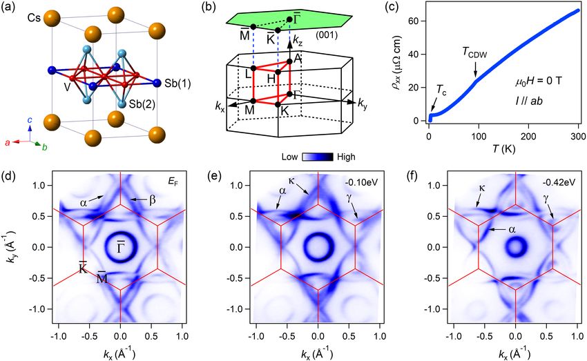
FIG. 1: Single crystal and FS topology of CsV3 Sb5 (T = 1.4 K).
(a) Schematic crystal structure of CsV3 Sb5 in the pristine phase. (b) are non-degenerate, then define the middle and inner constant-
Bulk BZ and corresponding 2D BZ projected on (001) surface in the energy sheets around K̄, respectively [Fig. 1(e)]. After further
pristine phase. The high-symmetry points are indicated. (c) Temper- decreasing the energy to -0.42 eV, which corresponds to the
ature dependence of the resistivity ρ xx at µ0 H = 0 T, where the onsets lower branches of the Dirac-cone structures, the α and κ bands
of CDW transition (T CDW ) and superconducting transition (T c ) are evolve into the middle and outer contours, respectively, while
observed. (d)-(f) Constant-energy ARPES intensity plots obtained the γ band still describes the inner pocket around K̄ [Fig. 1(f)].
by integrating the photoemission intensity within EF ± 20 meV at
As suggested by the theoretical calculations in the CDW
binding energies of 0, -0.10, and -0.42 eV, respectively. The pho-
ton energy for measurement is 95 eV. The red solid lines indicate the phase, which is found to favor the inverse Star of David dis-
pristine BZs. tortion energetically, the band structure is strongly modified
around K̄ as compared to that in the pristine phase [43]. The
most prominent reconstruction is a large gap opening at the
found in the Supplemental Material [53]. As shown in Fig. Dirac-like crossing located above EF along the Γ̄-K̄ direction.
1(a), the pristine phase of CsV3 Sb5 crystallizes in a layered By comparing our experimental data with the calculations, the
hexagonal structure with space group P6/mmm (No. 191) crossing corresponds to the one between the κ and γ bands. To
[20, 21, 23, 24, 39], which consists of an alternative stacking study the CDW-related gap opening along the Γ̄-K̄ direction,
of Cs layer and V-Sb slab along the c axis. The 2D kagome we use the photon energy of 50 eV, for the balance between
lattice is formed by V atoms coordinated by Sb atoms, which
can be further categorized into two kinds of Sb sites: in-plane
Sb(1) sites occupy the centers of the V hexagons, and out-
of-plane Sb(2) sites locate below and above the centers of V
triangles. The schematic 3D Brillouin zone (BZ) of pristine
phase and 2D projected one on the (001) surface are presented
in Fig. 1(b). According to previous ARPES studies with vari-
able photon energies, the electronic structure of AV3 Sb5 fam-
ily shows quasi-2D nature [50, 51], we hereafter use the deno-
tation of high-symmetry points in 2D BZ for convenience. In
Fig. 1(c), the zero-field resistivity exhibits metallic behavior
above the superconducting transition temperature (T c ∼ 2.5 K)
except a distinct kink at ∼92 K, indicating the onset of CDW
transition [39].
The constant-energy ARPES images at binding energies of
0, -0.10, and -0.42 eV are displayed in Figs. 1(d)-1(f), respec-
tively, exhibiting the hexagonal symmetry and network topol-
ogy with corner-sharing triangles expected from the kagome
lattice. Focusing on the FS around K̄, with monotonically
decreasing the energy, the two Fermi contours (α and β) grad-
ually evolve into three sheets (α, κ, and γ). The evolution be- FIG. 2: Overall band structure of CsV3 Sb5 (T = 1.4 K). (a),(b) Pho-
havior indicates that there are three bands dispersing around toemission intensity plot and corresponding second derivative plot
K̄, and two of them (κ and γ) could be degenerate near EF . along the Γ̄-K̄- M̄ direction taken with 95-eV photons, respectively.
The three linearly dispersive bands around K̄ are denoted as α, κ, and
To further unravel the underlying band structure, we record
γ, respectively, indicated by the blue dashed lines. (c),(d) Same as
the ARPES spectra along the Γ̄-K̄- M̄ and Γ̄- M̄ directions. The (a),(b) recorded along the Γ̄- M̄ direction.3
FIG. 3: CDW-induced peak-dip-hump structure and flat band in
CsV3 Sb5 . (a) ARPES intensity plot (T = 1.4 K) measured along
cut #1 (Γ̄-K̄ direction), which is illustrated by the white arrow in the
inset, with 50-eV photons. Besides the α, κ, and γ bands, a flat band
close to EF is denoted as β, where the black dots are determined FIG. 4: FS nesting scenario of the CDW in CsV3 Sb5 . (a),(b) Sketches
from the EDCs in (b). Inset: Sketches of the inner FS around K̄ with of the FSs (thick solid curves) above and below T CDW together with
pristine BZ. (b)-(d) EDC plots of (a) taken at T = 1.4, 5, and 23 K, the folded ones (thin dashed curves) by the in-plane 2 × 2 charge
respectively. (e)-(h) Same as (a)-(d) recorded along cut #2, which is ordering wave vector, respectively. (c)-(e) Cartoon of the band struc-
illustrated by the white arrow in the inset of (e). ture along the Γ̄-K̄ direction above [(c),(d)] and below T CDW [(e)],
respectively. The α*, κ*, and γ* bands (grey and green solid lines)
high energy resolution and scan area in momentum space, to represent the original band structure in the pristine phase, and the α’,
κ’, and γ’ bands (grey and green dashed lines) are the corresponding
record the intensity in the second BZ. As shown in Fig. 3(a), folded band structure with respect to the momentum cut, where the
the κ and γ bands are clearly observed near EF in contrast to vertical dashed line locates in (d), connecting adjacent M̄ points.
that measured in the first BZ [Figs. 2(a) and 2(b)]. Further,
we reveal that the κ and γ bands cross below EF and there
is an almost flat feature close to EF (denoted as β) separated spectral weight in the dip structure gradually increases. The
by depletion of intensity, pointing to a possible gap opening. redistribution of spectral weight upon temperature may be due
In order to quantitatively examine the band structure and gap to the thermal peak broadening, showing that the peak-dip-
opening, the corresponding energy distribution curve (EDC) hump structure is temperature sensitive and only visible deep
plot is presented in Fig. 3(b). By tracing the peak positions in the CDW state.
of EDCs, we can determine the detailed band dispersions. In- The origin of the peak-dip-hump feature and flat band close
dicated by the black curve, a distinct energy gap of ∼30 meV to EF can be well accounted for by the FS nesting scenario.
is resolved between the β band (∼0.02 eV below EF ) and the From a Peierls perspective, the electronic susceptibility would
κ/γ band, where the degeneracy occurs at ∼0.05 eV below EF . develop a logarithmic divergence singularity at some well
Intriguingly, we observe a peak-dip-hump feature around the nested FS sheets, hence results in a CDW transition [54]. In
energy gap, and the lineshape is contributed by the dispersion- this picture, the in-plane 2 × 2 charge ordering wave vector
less β band close to EF (peak) and the linearly dispersive κ/γ qCDW = (π, 0) of CsV3 Sb5 can connect the electronic states
band at higher binding energy (hump). at neighboring M̄ points, then the inter-band scattering would
To further determine how the energy gap and the peak-dip- cause CDW [43]. To examine the nesting property of the over-
hump structure distribute in momentum space, we perform a all FS topology, we sketch the FS above T CDW and fold it by
similar measurement along cut #2, illustrated by the white ar- two representative qCDW as shown in Fig. 4(a). One can ob-
row in the inset of Fig. 3(e). The gap opening of ∼30 meV and tain that nearly perfect nestings exist between the original γ*
the peak-dip-hump lineshape exhibit little change, as shown in and folded α’ as well as the original α* and folded γ’. Con-
Figs. 3(e) and 3(f). Consequently, these CDW-related features sequently, upon entering the CDW phase, the interactions be-
are uniformly distributed around K̄ (momentum cuts along tween nested bands result in gap opening and reconstructed
other directions around K̄ show similar behaviors, not shown FS in the CDW BZ as schematically shown in Fig. 4(b).
here). Then we carry out the temperature-dependent study of However, since the modulation potential of CDW is weak in
the band structure along cuts #1 [Figs. 3(b)-3(d)] and #2 [Figs. CsV3 Sb5 [44], such reconstructions in the small CDW BZs
3(f)-3(h)]. As the temperature is increased from 1.4 K to 23 K, are not observed [thin dashed curves in Fig. 4(b)]. The pris-
one can obtain that the energy gap remains unchanged, while tine and CDW phases host similar FS topologies [thick solid
the peak structure close to EF becomes less prominent and the curves in Figs. 4(a) and 4(b)], this is further supported by the4
similar FS in the pristine phase reported in Ref. [50]. Thus, the flat band feature close to EF . The occurrence of this CDW-
the charge compensation in the pristine phase is little affected related flat band is also energetically favorable as illustrated in
by the band folding effect associated with CDW due to the Fig. S3 [53]. As is the case for most known superconductors,
sizes of original FS components do not change significantly. the near-EF DOS boosted by a saddle point or an extended flat
Since the band folding by qCDW is equivalent to that along region of the dispersion could play an important role in the
the Γ̄-K̄ direction with respect to the momentum cut connect- superconductivity [56, 57]. We believe that the onset of su-
ing neighboring M̄ points, we show the band structure car- perconductivity in CsV3 Sb5 is closely related to the enhanced
toons along the Γ̄-K̄ direction to clarify the detailed mech- DOS associated with the flat band, which defines majority of
anism. We reconstruct the band structure (α*, κ*, and γ*) the FS in the CDW state.
above T CDW in Fig. 4(c) and plot them in Fig. 4(d) together In summary, we demonstrate a peak-dip-hump lineshape re-
with the folded bands (α’, κ’, and γ’) expected to emerge due lated to the isotropic CDW gap opening around K̄ deep in the
to CDW order. It is seen that α’ will interact with γ* just CDW state of CsV3 Sb5 . We observe that linearly dispersive
below EF , resulting in the CDW gap opening which leads to Dirac bands contribute to the hump structure, and the peak
the flat band β and peak-dip-hump lineshape. The κ* band structure corresponds to a dispersionless flat band close to EF .
does not have a “partner” to interact with in the CDW state These spectral features arise from the nearly perfect FS nest-
and therefore remains as is, smearing out the peak-dip-hump ings and the flat band provides high DOS promoting the onset
lineshape at lower momentum values. Thus, the κ feature in of superconductivity. Our results put strong constraints on the
Fig. 4(e) actually represents a superposition of κ* and α’. theoretical model for solving the origin of CDW and super-
Analogous peak-dip-hump structure is not resolved at equiv- conductivity in AV3 Sb5 compounds.
alent momentum [∼0.4 Å−1 in Figs. 3(a) and 3(e)] where α* This work was in part supported by the Deutsche
should interact with γ’, because the intensity of the former Forschungsgemeinschaft under Grants SFB 1143 (project
is very strong and the latter, being folded of γ*, is vanish- C04). R.L. was supported by National Natural Science Foun-
ingly weak. Most of the folded bands are hardly observed in dation of China (Grant No. 11904144). A.K., B.B., and S.B.
CsV3 Sb5 because strongest features (e.g. α’) nearly overlap acknowledge the support from BMBF via project UKRATOP.
with already existing ones (e.g. κ*) and the modulation po- H.C.L. was supported by National Natural Science Founda-
tential appears to be weak [44]. The formation of the CDW tion of China (Grants No. 11822412 and No. 11774423),
gap can explain the band reconstructions reported in a recent Ministry of Science and Technology of China (Grants No.
ARPES study on CsV3 Sb5 [50]. The gap size of ∼30 meV is 2018YFE0202600 and No. 2016YFA0300504), and Beijing
comparable with that in previous STM [25] and ARPES stud- Natural Science Foundation (Grant No. Z200005). E.S. was
ies [49], but smaller than that determined by an optical spec- support by the Würzburg-Dresden Cluster of Excellence on
troscopy measurement [36]. Note that theory predicts also a Complexity and Topology in Quantum Matter–ct.qmat (EXC
spin-orbit coupling (SOC) induced gap at the crossing of κ* 2147, project-id 390858490).
and γ* in the pristine phase [43]. Existing ARPES data imply R.L., A.F., and Q.W.Y. contributed equally to this work.
that this SOC gap is centered only slightly above EF at T >
T CDW [50]. As schematically illustrated in Fig. S1 [53], the
β feature appears to be flattened by both gaps – from SOC
gap above and from CDW gap below. However, since weaker
∗
features are not clearly resolved in our spectra, we leave only lourui@lzu.edu.cn
†
a.fedorov@ifw-dresden.de
most pronounced of them in Fig. 4(e). Our data, together with ‡
hlei@ruc.edu.cn
earlier observations [25, 49, 50], suggest that the theory may §
s.borisenko@ifw-dresden.de
overestimate both the energy position of SOC gap and the size [1] Y. Deng, Y. Yu, M. Shi, Z. Guo, Z. Xu, J. Wang, X. Chen, and
of CDW gap. Y. Zhang, Science 367, 895 (2020).
Before closing, we discuss the implication of our results [2] M. Serlin, C. L. Tschirhart, H. Polshyn, Y. Zhang, J. Zhu, K.
on the underlying superconductivity. Our observation of the Watanabe, T. Taniguchi, L. Balents, and A. F. Young, Science
367, 900 (2020).
CDW gap opening below T c demonstrates the coexistence of
[3] C. Liu, S.-C. Zhang, and X.-L. Qi, Annu. Rev. Condens. Matter
CDW and superconductivity in CsV3 Sb5 . We further make an Phys. 7, 301 (2016).
attempt to detect the superconducting gap in the small CDW [4] P. Zhang, K. Yaji, T. Hashimoto, Y. Ota1, T. Kondo, K.
BZ. As presented in Fig. S2 [53], a leading edge shift of ∼0.3- Okazaki, Z. Wang, J. Wen, G. D. Gu, H. Ding, and S. Shin,
0.4 meV is observed on the electron FS at BZ center when go- Science 360, 182 (2018).
ing across T c , showing the signature of superconducting gap [5] D. Wang, L. Kong, P. Fan, H. Chen, S. Zhu, W. Liu, L. Cao,
opening. The gap size is consistent with that in recent STM Y. J. Sun, S. Du, J. Schneeloch, R. Zhong, G. D. Gu, L. Fu, H.
Ding, and H.-J. Gao, Science 362, 333 (2018).
studies [34, 42]. In a Bilbro-McMillan partial gaping scenario,
[6] C. Chen, Q. Liu, T. Z. Zhang, D. Li, P. P. Shen, X. L. Dong,
the CDW would strongly compete with superconductivity for Z.-X. Zhao, T. Zhang, and D. L. Feng, Chin. Phys. Lett. 36,
the FS [55]. However, the electronic states at EF are not de- 057403 (2019).
pleted by the CDW order here. Instead, the formation of CDW [7] S. Zhu, L. Kong, L. Cao, H. Chen, M. Papaj, S. Du, Y. Xing, W.
seems to prepare the system for superconductivity by creating Liu, D. Wang, C. Shen, F. Yang, J. Schneeloch, R. Zhong, G.5
D. Gu, L. Fu, Y. Zhang, H. Ding, and H.-J. Gao, Science 367, F. Guo, X. F. Yang, and S. Y. Li, arXiv:2102.08356 (2021).
189 (2020). [28] H. Zhao, H. Li, B. R. Ortiz, S. M. L. Teicher, T. Park, M.
[8] G. Xu, B. Lian, P. Tang, X.-L. Qi, and S.-C. Zhang, Phys. Rev. Ye, Z. Wang, L. Balents, S. D. Wilson, and I. Zeljkovic,
Lett. 117, 047001 (2016). arXiv:2103.03118 (2021).
[9] W. Ruan, X. Li, C. Hu, Z. Hao, H. Li, P. Cai, X. J. Zhou, D.-H. [29] W. Duan, Z. Nie, S. Luo, F. Yu, B. R. Ortiz, L. Yin, H. Su, F.
Lee, and Y. Wang, Nat. Phys. 14, 1178 (2018). Du, A. Wang, Y. Chen, X. Lu, J. Ying, S. D. Wilson, X. Chen,
[10] D. F. Agterberg, J. C. S. Davis, S. D. Edkins, E. Fradkin, D. Y. Song, and H. Yuan, arXiv:2103.11796 (2021).
Harlingen, S. A. Kivelson, P. A. Lee, L. Radzihovsky, J. M. [30] X. Chen, X. Zhan, X. Wang, J. Deng, X. Liu, X. Chen, J. Guo,
Tranquada, and Y. Wang, Annu. Rev. Condens. Matter Phys. and X. L. Chen, Chin. Phys. Lett. 38, 057402 (2021).
11, 231 (2020). [31] Z. Zhang, Z. Chen, Y. Zhou, Y. Yuan, S. Wang, J. Wang, H.
[11] J. Yin, W. Ma, T. A. Cochran, X. Xu, S. S. Zhang, H.-J. Tien, Yang, C. An, L. Zhang, X. Zhu, Y. Zhou, X. Chen, J. Zhou, and
N. Shumiya, G. Cheng, K. Jiang, B. Lian, Z. Song, G. Chang, Z. Yang, arXiv:2103.12507 (2021).
I. Belopolski, D. Multer, M. Litskevich, Z. Cheng, X. P. Yang, [32] Z. Liang, X. Hou, W. Ma, F. Zhang, P. Wu, Z. Zhang, F.
B. Swidler, H. Zhou, H. Lin, T. Neupert, Z. Wang, N. Yao, T.- Yu, J.-J. Ying, K. Jiang, L. Shan, Z. Wang, and X.-H. Chen,
R. Chang, S. Jia, and M. Z. Hasan, Nature (London) 583, 533 arXiv:2103.04760 (2021).
(2020). [33] H. X. Li, T. T. Zhang, Y. Y. Pai, C. Marvinney, A. Said, T.
[12] Q. Wang, K. J. Neubauer, C. Duan, Q. Yin, S. Fujitsu, H. Yilmaz, Q. Yin, C. Gong, Z. Tu, E. Vescovo, R. G. Moore,
Hosono, F. Ye, R. Zhang, S. Chi, K. Krycka, H. C. Lei, and S. Murakami, H. C. Lei, H. N. Lee, B. Lawrie, and H. Miao,
P. C. Dai, Phys. Rev. B 103, 014416 (2021). arXiv:2103.09769 (2021).
[13] T. Das, J.-X. Zhu, and M. J. Graf, Phys. Rev. Lett. 108, 017001 [34] H. Chen, H. Yang, B. Hu, Z. Zhao, J. Yuan, Y. Xing, G. Qian,
(2012). Z. Huang, G. Li, Y. Ye, Q. Yin, C. Gong, Z. Tu, H. Lei, S. Ma,
[14] A. A. Kordyuk, S. V. Borisenko, T. K. Kim, K. A. Nenkov, M. H. Zhang, S. Ni, H. Tan, C. Shen, X. Dong, B. Yan, Z. Wang,
Knupfer, J. Fink, M. S. Golden, H. Berger, and R. Follath, Phys. and H.-J. Gao, arXiv:2103.09188 (2021).
Rev. Lett. 89, 077003 (2002). [35] S. Ni, S. Ma, Y. Zhang, J. Yuan, H. Yang, Z. Lu, N. Wang,
[15] A. Damascelli and Z.-X. Shen, Rev. Mod. Phys. 75, 473 (2003). J. Sun, Z. Zhao, D. Li, S. Liu, H. Zhang, H. Chen, K. Jin, J.
[16] Z. K. Liu, R.-H. He, D. H. Lu, M. Yi, Y. L. Chen, M. Cheng, L. Yu, F. Zhou, X. Dong, J. Hu, H.-J. Gao, and Z.-X.
Hashimoto, R. G. Moore, S.-K. Mo, E. A. Nowadnick, J. Hu, T. Zhao, Chin. Phys. Lett. 38, 057403 (2021).
J. Liu, Z. Q. Mao, T. P. Devereaux, Z. Hussain, and Z.-X. Shen, [36] X. Zhou, Y. Li, X. Fan, J. Hao, Y. Dai, Z. Wang, Y. Yao, and
Phys. Rev. Lett. 110, 037003 (2013). H.-H. Wen, arXiv:2104.01015 (2021).
[17] N. Mannella, W. L. Yang, X. J. Zhou, H. Zheng, J. F. Mitchell, [37] Y. Xiang, Q. Li, Y. Li, W. Xie, H. Yang, Z. Wang, Y. Yao, and
J. Zaanen, T. P. Devereaux, N. Nagaosa, Z. Hussain, and Z.-X. H.-H. Wen, arXiv:2104.06909 (2021).
Shen, Nature (London) 438, 474 (2005). [38] C. Mu, Q. W. Yin, Z. Tu, C. Gong, H. C. Lei, Z. Li, and J.-L.
[18] N. Mannella, W. L. Yang, K. Tanaka, X. J. Zhou, H. Zheng, J. F. Luo, arXiv:2104.06698 (2021).
Mitchell, J. Zaanen, T. P. Devereaux, N. Nagaosa, Z. Hussain, [39] Y. Fu, N. Zhao, Z. Chen, Q. Yin, Z. Tu, C. Gong, C. Xi, X. Zhu,
and Z.-X. Shen, Phys. Rev. B 76, 233102 (2007). Y. Sun, K. Liu, and H. C. Lei, arXiv:2104.08193 (2021).
[19] L. Ye, M. Kang, J. Liu, F. Cube, C. R. Wicker, T. Suzuki, [40] D. W. Song, L. X. Zheng, F. H. Yu, J. Li, L. P. Nie, M. Shan, D.
C. Jozwiak, A. Bostwick, E. Rotenberg, D. C. Bell, L. Fu, Zhao, S. J. Li, B. L. Kang, Z. M. Wu, Y. B. Zhou, K. L. Sun, K.
R. Comin, and J. G. Checkelsky, Nature (London) 555, 638 Liu, X. G. Luo, Z. Y. Wang, J. J. Ying, X. G. Wan, T. Wu, and
(2018). X.-H. Chen, arXiv:2104.09173 (2021).
[20] B. R. Ortiz, L. C. Gomes, J. R. Morey, M. Winiarski, M. Bor- [41] C. C. Zhu, X. F. Yang, W. Xia, Q. W. Yin, L. S. Wang, C. C.
delon, J. S. Mangum, I. W. H. Oswald, J. A. Rodriguez-Rivera, Zhao, D. Z. Dai, C. P. Tu, B. Q. Song, Z. C. Tao, Z. J. Tu, C.
J. R. Neilson, S. D. Wilson, E. Ertekin, T. M. McQueen, and E. S. Gong, H. C. Lei, Y. F. Guo, and S. Y. Li, arXiv:2104.14487
S. Toberer, Phys. Rev. Materials 3, 094407 (2019). (2021).
[21] B. R. Ortiz, S. M. L. Teicher, Y. Hu, J. L. Zuo, P. M. Sarte, E. [42] H. Xu, Y. Yan, R. Yin, W. Xia, S. Fang, Z. Chen, Y. Li, W.
C. Schueller et al., Phys. Rev. Lett. 125, 247002 (2020). Yang, Y. Guo, and D. L. Feng, arXiv:2104.08810 (2021).
[22] S.-Y. Yang, Y. Wang, B. R. Ortiz, D. Liu, J. Gayles, E. [43] H. X. Tan, Y. Liu, Z. Wang, and B. H. Yan, arXiv:2103.06325
Derunova, R. Gonzalez-Hernandez, L. Šmejkal, Y. Chen, S. S. (2021).
P. Parkin, S. D. Wilson, E. S. Toberer, T. McQueen, and M. N. [44] Z. X. Wang, Q. Wu, Q. W. Yin, Z. J. Tu, C. S. Gong, T. Lin, Q.
Ali, Sci. Adv. 6, eabb6003 (2020). M. Liu, L. Y. Shi, S. J. Zhang, D. Wu, H. C. Lei, T. Dong, and
[23] Q. Yin, Z. Tu, C. Gong, Y. Fu, S. Yan, and H. C. Lei, Chin. N. L. Wang, arXiv:2105.11393 (2021).
Phys. Lett. 38, 037403 (2021). [45] X. L. Feng, K. Jiang, Z. Wang, and J. P. Hu, arXiv:2103.07097
[24] B. R. Ortiz, P. M. Sarte, E. M. Kenney, M. J. Graf, S. M. L. (2021).
Teicher, R. Seshadri, and S. D. Wilson, Phys. Rev. Materials 5, [46] M. M. Denner, R. Thomale, and T. Neupert, arXiv:2103.14045
034801 (2021). (2021).
[25] Y. Jiang, J. Yin, M. Denner, N. Shumiya, B. R. Ortiz, G. Xu, Z. [47] K. Nakayama, Y. Li, M. Liu, Z. Wang, T. Takahashi, Y. Yao,
Guguchia, J. He, M. Hossain, X. Liu, J. Ruff, L. Kautzsch, S. and T. Sato, arXiv:2104.08042 (2021).
S. Zhang, G. Chang, I. Belopolski, Q. Zhang, T. A. Cochran, [48] Z. G. Wang, S. Ma, Y. Zhang, H. Yang, Z. Zhao, Y. Ou, Y. Zhu,
D. Multer, M. Litskevich, Z. Cheng, X. P. Yang, Z. Wang, S. Ni, Z. Lu, H. Chen, K. Jiang, L. Yu, Y. Zhang, X. Dong, J.
R. Thomale, T. Neupert, S. D. Wilson, and M. Z. Hasan, Hu, H.-J. Gao, and Z.-X. Zhao, arXiv:2104.05556 (2021).
arXiv:2012.15709 (2020). [49] M. Kang, S. Fang, J.-K. Kim, B. R. Ortiz, J. Yoo, B.-G. Park, S.
[26] F. H. Yu, T. Wu, Z. Y. Wang, B. Lei, W. Z. Zhuo, J. J. Ying, and D. Wilson, J.-H. Park, and R. Comin, arXiv:2105.01689 (2021).
X. H. Chen, arXiv:2102.10987 (2021). [50] Y. Hu, S. M. L. Teicher, B. R. Ortiz, Y. Luo, S. Peng, L. Huai,
[27] C. C. Zhao, L. S. Wang, W. Xia, Q. W. Yin, J. M. Ni, Y. Y. J. Z. Ma, N. C. Plumb, S. D. Wilson, J.-F. He, and M. Shi,
Huang, C. P. Tu, Z. C. Tao, Z. J. Tu, C. S. Gong, H. C. Lei, Y. arXiv:2104.12725 (2021).6
[51] Z. Liu, N. Zhao, Q. Yin, C. Gong, Z. Tu, M. Li, W. Song, Z. [54] G. Grüner, Density Waves in Solids (Addison-Wesley, Reading,
Liu, D. Shen, Y. Huang, K. Liu, H. C. Lei, and S.-C. Wang, MA, 1994).
arXiv:2104.01125 (2021). [55] G. Bilbro and W. L. McMillan, Phys. Rev. B 14, 1887 (1976).
[52] S. Cho, H. Ma, W. Xia, Y. Yang, Z. Liu, Z. Huang, Z. Jiang, [56] S. V. Borisenko, V. B. Zabolotnyy, D. V. Evtushinsky, T. K.
X. Lu, J. Liu, Z. Liu, J. Jia, Y. Guo, J. Liu, and D. W. Shen, Kim, I. V. Morozov, A. N. Yaresko, A. A. Kordyuk, G. Behr,
arXiv:2105.05117 (2021). A. Vasiliev, R. Follath, and B. Büchner, Phys. Rev. Lett. 105,
[53] See Supplemental Material for detailed experimental methods 067002 (2010).
of crystal growth and ARPES measurements, origin of the flat [57] S. Borisenko, Nat. Mater. 12, 600 (2013).
band feature close to EF , signature of superconducting gap
opening, and energy gain of the occurrence of CDW.You can also read


