Comparison of measured and simulated spin-wave mode spectra of magnetic nanostructures
←
→
Page content transcription
If your browser does not render page correctly, please read the page content below

Comparison of measured and simulated
spin-wave mode spectra of magnetic
nanostructures
Cite as: Appl. Phys. Lett. 118, 012408 (2021); https://doi.org/10.1063/5.0039188
Submitted: 30 November 2020 . Accepted: 20 December 2020 . Published Online: 06 January 2021

  H. T. Nembach,      R. D. McMichael, M. L. Schneider, J. M. Shaw, and   T. J. Silva

ARTICLES YOU MAY BE INTERESTED IN

Beyond the gyrotropic motion: Dynamic C-state in vortex spin torque oscillators
Applied Physics Letters 118, 012404 (2021); https://doi.org/10.1063/5.0029083

Bias-field-free high frequency microwave emission of spin-transfer nano-oscillator with
magnetizations all in-plane
Applied Physics Letters 118, 012405 (2021); https://doi.org/10.1063/5.0031507

Signal detection based on the chaotic motion of an antiferromagnetic domain wall
Applied Physics Letters 118, 012402 (2021); https://doi.org/10.1063/5.0034997

Appl. Phys. Lett. 118, 012408 (2021); https://doi.org/10.1063/5.0039188                  118, 012408

© 2021 Author(s).
Applied Physics Letters                                                                            ARTICLE            scitation.org/journal/apl

    Comparison of measured and simulated spin-wave
    mode spectra of magnetic nanostructures
    Cite as: Appl. Phys. Lett. 118, 012408 (2021); doi: 10.1063/5.0039188
    Submitted: 30 November 2020 . Accepted: 20 December 2020 .
    Published Online: 6 January 2021

    H. T. Nembach,1,2,a)             R. D. McMichael,3         M. L. Schneider,2 J. M. Shaw,2 and T. J. Silva2

    AFFILIATIONS
    1
        JILA, University of Colorado, Boulder, Colorado 80309, USA
    2
        Quantum Electromagnetics Division, National Institute of Standards and Technology, Boulder, Colorado 80305, USA
    3
        Nanoscale Device Characterization Division, National Institute of Standards and Technology, Gaithersburg, Maryland 20899, USA

    a)
         Author to whom correspondence should be addressed: hans.nembach@nist.gov

    ABSTRACT
    Motivated by the importance of magnetization dynamics in nanomagnets for the development and optimization of magnetic devices and
    sensors, we measured and modeled spin wave spectra in patterned elliptical nanomagnets. Ferromagnetic resonance spectra for multiple
    nanomagnets of Ni80Fe20, fabricated by electron-beam lithography to have nominal short-axes of 200 nm or 100 nm, were measured by use
    of heterodyne magneto-optical microwave microscopy. Scanning electron microscope images taken of the same nanomagnets were used to
    define element shapes for micromagnetic simulations. The measured spectra show significant differences between nominally identical nano-
    magnets, which could be only partially attributed to uncontrolled shape variations in the patterning process, as evidenced by the limited
    agreement between the measured and simulated spectra. Agreement between measurements and simulations was improved by including a
    zone of reduced magnetization and exchange at the edges of the nanomagnets in the simulations. Our results show that the reduction of
    shape variations between individual magnetic random-access memory elements can potentially improve their performance. However, unam-
    biguous determination of materials parameters in nanomagnets based on analysis and modeling of spin wave spectra remains problematic.
    Published under license by AIP Publishing. https://doi.org/10.1063/5.0039188

          Nanomagnets are the building blocks of hard disk drive read                   We investigate the role of shape imperfections on the mode
    heads1 and magnetic random access memory (MRAM)2–4 and have                   dynamics in single nanomagnets. As is known, shape imperfections
    promise for emerging applications in probabilistic5–7 and neuromor-           give rise to spatially varying demagnetizing fields. Such local variations
    phic computing.8–10 These applications all require the understanding          in the demagnetization fields can lead to nucleation sites for the
    and exploitation of high-speed dynamics within the nanomagnets.               switching.12 It has been demonstrated that higher write error rates
    MRAM has been used in specialized hardware for several years but is           are correlated with the existence of more resonances in spin-torque
    poised to enter a much broader range of applications as embedded              ferromagnetic resonance (ST-FMR) measurements of devices.13 These
    MRAM. Some of the critical parameters for MRAM devices include                additional resonances can be the result of deviations from the ideal
    write error rate and thermal stability. The write error rate is the rate of   shape of the device.
    failed switching events for a given number of attempts. High write                  In addition to shape imperfections, non-uniformity in materials
    error rates require more computation overhead with respect to error           parameters across a device can also be introduced during the pattern-
    correction, which will tend to drive up the overall cost. Thermal stabil-     ing process. For example, transmission electron microscopy images
    ity determines the data retention time and is proportional to the             have found a ring of about 12 nm–20 nm of altered contrast at the
    energy barrier, which prevents undesired thermal fluctuations between          edges of (Co/Pd)n multilayer nanomagnets,14 which indicates redepo-
    the two magnetic states. A high energy barrier provides high thermal          sition and intermixing as a result of the lithography. The width and
    stability though typically at the expense of larger currents required for     the severity of the non-uniformities at the edges depend on the details
    write operations.4 A detailed understanding of the switching process is       of the patterning process. It has also been shown that the stiffness
    critical to guide the design of MRAM.11 The switching process                 fields and, consequently, the resonance fields for localized spin-wave
    depends on the physical switching mechanism in conjunction with               modes in Ni80Fe20 stripes depend on the sidewall angle.15 This sug-
    both the material parameters and the shape of the MRAM cell.                  gests that the details of spin-wave modes near patterned edges are

Appl. Phys. Lett. 118, 012408 (2021); doi: 10.1063/5.0039188                                                                                    118, 012408-1
Published under license by AIP Publishing
Applied Physics Letters                                                                          ARTICLE              scitation.org/journal/apl

    highly susceptible to both edge damage and unintended shape varia-        by a 300 eV Ar ion mill. Finally, the remaining DLC was removed by a
    tions. Nembach et al. demonstrated that the number of localized           second O2 plasma etch. The ellipses were imaged with an SEM as
    modes could be increased by intentionally distorting the elliptical       shown in the insets in the left columns of Figs. 2 and 3. Images of addi-
    shape when measuring large ensembles of nanomagnets by use of             tional nanomagnets are shown in the supplementary material.
    low-resolution Brillouin light scattering spectroscopy.16 However,              The spin wave mode spectra of the magnetization dynamics were
    ensemble measurements are prone to interpretation difficulties when        measured with a heterodyne magneto-optical microwave microscope
    nanomagnet variations cause significant line broadening.17                 (H-MOMM); see Fig. 1 for a simplified sketch of the setup.18 The
    Measurements of individual nanomagnets are required to fully under-       H-MOMM employs two frequency tunable single frequency lasers
    stand how much variation in the localized spin-wave spectra for nomi-     operating at 532 nm. Part of both laser beams is split-off and focused
    nally identical structures actually exists.                               onto a high-speed photodiode, where they generate microwaves at the
          A heterodyne magneto-optical Kerr effect microscope (H-             difference frequency of both laser beams. The microwaves are ampli-
    MOMM) is an optical tool for the study of spin-wave spectra of            fied and fed into a coplanar waveguide, with the sample located on
    well-spaced individual nanomagnets.18 Other methods to measure            top. One of the laser beams is focused with an objective lens with a
    magnetization dynamics in sub-micron magnetic elements and                NA ¼ 0.9 onto the sample. When the external magnetic field meets
    devices are scanning transmission x-ray microscopy (STXM),19,20           the resonance condition, the precessing magnetization modulates the
    Brillouin Light Scattering microscopy,21 ST-FMR and noise mea-            polarization of the back-reflected light due to the magneto-optical
    surements on devices,22,23 magnetic-resonance force microscopy            Kerr effect. The back-reflected light is then mixed with the other laser
    (MRFM),24,25 and the time-resolved magneto-optical Kerr effect            beam at a beam splitter cube. The two out-going beams are finally
    (TR-MOKE).26 The H-MOMM was previously used to investigate                focused onto a differential detector. As a result of the demodulation of
    damping enhancement in patterned nanomagnets as small as                  the AC signal achieved by remixing the two laser beams, the measured
    100 nm, where the spatial curvature of a given spin-wave mode had         DC signal on the differential detector is proportional to the amplitude
    a direct impact on the frequency dependence of the measured line-         of the Kerr rotation generated by the precessing magnetization of the
    width.27 In the present study, we apply the H-MOMM to survey the          back-reflected laser beam. The H-MOMM allows us to measure nano-
    spin-wave spectra of nominally identically nanomagnets in sparse          magnets fabricated from individual magnetic layers, which are the
    patterned arrays. The spectra are surprisingly variable, given the tol-   building blocks of magnetic logic and memory devise. This is in con-
    erances of the lithographic processing employed. It appears as if         trast to electrical measurements, which can be, for example, based on
    each nanomagnet has its own spectroscopic fingerprint that makes           ST-FMR.22,28 These measurements require at least two magnetic
    it uniquely identifiable in spite of the process control. To understand    layers, the reference and the free layer. In general, ST-FMR measure-
    how the spin-wave spectra can vary so much, we used scanning              ments probe the performance of the complete device and, as such,
    electron microscopy (SEM) as a dimensioning tool to image the             provide complementary information to H-MOMM measurements on
    same nanomagnets that were used for the H-MOMM measure-                   the building blocks. The impact of process-induced edge damage on
    ments, and the dimensions obtained were then input to micromag-           spin-wave modes has been successfully measured with ST-FMR.13,29
    netic simulations. We obtained only qualitative agreement between               Representative spectra for the 200 nm and 100 nm nanomagnets
    the H-MOMM measurements and micromagnetics simulations,                   are shown in Figs. 2 and 3, respectively. The magnetic field was applied
    which implies that more subtle details associated with edge structure     along the long axis of the nanomagnets and the excitation frequency
    strongly affect the boundary conditions for the localized spin-wave       was 8:2 GHz. Most of the spectra for the 200 nm nanomagnets
    modes. As an example of such an edge detail that would not be             include one intense peak and two weaker peaks. Two peaks are visible
    apparent in SEM micrographs, we investigate how a simple grada-           in most of the 100 nm nanomagnets’ spectra. The nanomagnets within
    tion of magnetization near the edges of the nanomagnets can signifi-       each of these sets all have nominally the same dimensions. Spectra for
    cantly alter the simulated spectra. Our results confirm qualitatively
    that such gradients, in conjunction with shape variations, are suffi-
    cient to cause the variations in the spectra. This highlights the need
    for additional metrological tools to address how lithographic pat-
    terning affects the internal energetic landscape of patterned
    nanomagnets.
          In this work, we prepared two sets of Ni80Fe20 elliptical nano-
    magnets with nominal long axis lengths of 240 nm and 120 nm and
    short axes of 200 nm and 100 nm: thin-film layers of 3 nm Ta/10 nm
    Ni80Fe20/5 nm Si3N4 were dc-magnetron sputtered onto a sapphire
    substrate before a 15 nm diamond-like carbon (DLC) layer was depos-
    ited via ion-beam deposition in a separate vacuum chamber. Electron
    beam lithography was then used to expose a 100-nm-thick polymethyl
    methacrylate layer, which was developed in a methyl isobutyl ketone:
    isopropanol solution. A 5 nm Cr layer was then deposited and lifted
                                                                              FIG. 1. Sketch of the H-MOMM setup. The beams from the two single frequency
    off via ion beam deposition. The pattern was transferred to the DLC       lasers are combined at beam splitter 1 to generate the microwaves. The backre-
    layer via an O2 plasma etch before the Cr was removed with a wet          flected laser beam from the sample is mixed with laser 2 at beam splitter 2, before
    etch. The final pattern transfer to the Ni80Fe20 layer was accomplished    they are focused onto the differential detector.

Appl. Phys. Lett. 118, 012408 (2021); doi: 10.1063/5.0039188                                                                                        118, 012408-2
Published under license by AIP Publishing
Applied Physics Letters ARTICLE scitation.org/journal/apl
a ¼ 0:0074, and a uniform exchange length lex ¼ 5:69 nm, which cor-
responds to exchange stiffness A ¼ 13 pJ/m in full-magnetization cells.
The cell size was 1.92 1.92 10 nm3. To determine the shape for
modeled nanomagnets, grayscale SEM images of the nanomagnets
were converted into binary images using a thresholding algorithm.
The original SEM images, see insets of Figs. 2(a) and 2(c) and 3(a)
and 3(c), were given a Gaussian blur over 2.8 nm (6 pixels), and a
threshold value was determined using Otsu’s method.31 The resulting
sample boundaries for the respective nanomagnets are shown in the
insets of Figs. 2(b) and 2(d) and 3(b) and 3(d).
The simulated spectra were extracted from impulse response cal-
culations made at an array of applied field values in the experimental
range. The modeling also provides the spatial profile of the spin wave
modes; see the insets of Figs. 2(b) and 2(d) and 3(b) and 3(d). The spa-
tial profiles show that the strongest peak for the larger nanomagnet is
mainly localized in the center of the nanomagnet (center-mode),
whereas the two weaker modes are localized at the ends of the nano-
magnet (end-modes). For the smaller nanomagnets, only end-modes
are visible in the experimental range, but the model also produces a
FIG. 2. Spectra of two 200 nm nanomagnets measured at 8.2 GHz with the mag- center-mode at higher frequencies. The micromagnetic code does not
netic field applied along the long axis are shown in (a) and (c) together with SEM include any curvature dependent damping term, which would be
images of the respective nanomagnets. The corresponding spectra obtained from
micromagnetic simulations are shown in (b) and (d), where insets show the mod- necessary to accurately reproduce the experimental linewidth.27,32
eled mode profiles at the resonance peaks. The strongest peak corresponds to a In the larger nanomagnets one of the most striking differences
center-mode, and the two weaker peaks correspond to end-modes. The scale bars between measured and modeled spectra is that the resonance field
are 100 nm. The image outlines show the modeled sample shape as determined difference between the center- and the end-modes is much larger in
from the SEM images. the simulations. We ran additional simulations to check the impact of
edge damage, which can include angled sidewalls and reduced satura-
other nominally identical nanomagnets are provided in the supple- tion magnetization as a result of that intermixing may be responsible
mentary material. for these differences.15,33 In order to model damage as a zone of
We carried out micromagnetic simulations using the Object reduced magnetization at the edges, we started out with ideal ellipses
Oriented MicroMagnetic Framework (OommF).30 We used with dimensions of 262 nm 190 nm and 126 nm 90 nm, which
Ms ¼ 800 kA/m for the saturation magnetization, damping value were subdivided into 2 2 10 nm3 cells. We then reduced the mag-
netization at the edge by averaging the magnetization for each cell
over a disk with a set radius r, where r ranged from 2 nm to 8 nm. We
held the exchange length constant for the area of reduced magnetiza-
tion, which is equivalent to assuming that the exchange stiffness A
scales as Ms2 .
The results of these modified-edge simulations are shown in
Fig. 4. Panels (a) and (b) show spectra calculated for larger and smaller
ellipse sizes, respectively, with increasing edge damage from top to
bottom as indicated in the center images. In Fig. 4(a), the effect of
the reduced magnetization and exchange at the edges can be seen in
the simulated spectra as a slight increase in the resonance field for the
center-mode and a more pronounced decrease for the end-modes. A
higher sensitivity to the reduced magnetization at the edges is expected
for the end-modes because they are more strongly localized in the area
where the magnetization is reduced. The effect of reduced magnetiza-
tion for the end-modes in the smaller nanomagnets is similar; see
Fig. 4(b). The difference between the experimental spectra and the
simulated spectra can be reduced by introducing this small spatial var-
iation in the magnetization and exchange at the edges of the nanomag-
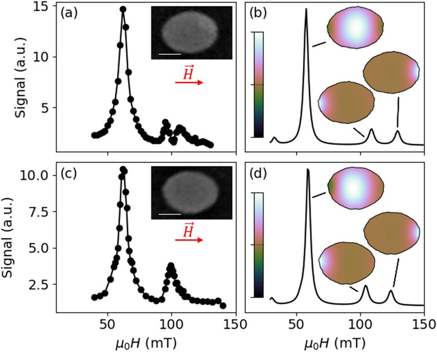
FIG. 3. Spectra of two 100 nm nanomagnets measured at 8.2 GHz with the mag- nets. The influence of the modified edges on the spatial profiles of the
netic field applied along the long axis are shown in (a) and (c) together with SEM center- and end-modes can be seen in the supplementary material.
images of the respective nanomagnets. The corresponding spectra obtained from
We are careful not to identify reduced edge magnetization as the
micromagnetic simulations are shown in (b) and (d), where insets show the mod-
eled mode profiles at the resonance peaks. The peaks observed at this frequency cause of differences between measured and simulated spectra, as
are end-modes. Scale bars are 100 nm, and the image outlines show the modeled other physical phenomena may produce similar effects. Edge modes
sample shape as determined from the SEM images. in transversely magnetized stripes share characteristics with the
Appl. Phys. Lett. 118, 012408 (2021); doi: 10.1063/5.0039188 118, 012408-3
Published under license by AIP Publishing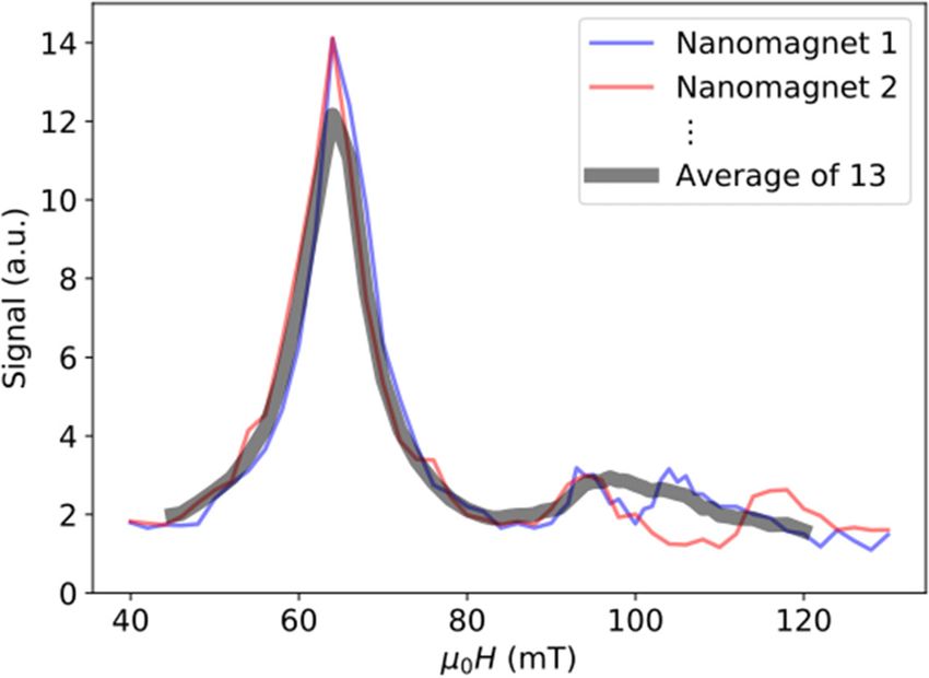
Applied Physics Letters                                                                                     ARTICLE               scitation.org/journal/apl

                                                                                         FIG. 5. The thick gray line is the average spectra of 13 different nanomagnets. The
                                                                                         red and blue traces represent two different spectra of individual nanomagnets.
     FIG. 4. Simulated spectra showing the effects of reduced magnetization at the
     edges. Spectra for symmetric, 262 nm 190 nm ellipses are plotted in (a) and for    when spatial variations of the magnetization and the exchange are
     126 nm  90 nm ellipses in (b). Only end-modes are visible for the smaller nano-    included in the simulations. However, without prior knowledge of the
     magnets. Due to the symmetry of the nanomagnets, the resonance fields of both
                                                                                         details of such spatial variations, it is challenging to extract materials
     end-modes are identical. Tapered magnetization profiles were created from ellipse
     images with moving averages over disks of radius r. The center images show the      parameters by matching experiment to simulations. Finally, this survey
     tapered Ms as red bar lengths and as grayscale. As magnetization near the edge      of nominally identical nanomagnets shows how measurements of the
     becomes diluted, center-modes [strong peaks in (a)] are largely unaffected, while   building blocks of MRAM devices can provide important insight into
     the edge modes (all other peaks) shift to lower fields.                              device performance. For example, it is difficult to achieve quantitative
                                                                                         matching of the measured dynamics to the simulations, while even the
    end-modes observed here, and the edge modes have been shown to be                    best process will have variations at the edges. At the same time, it is
    sensitive sidewall angles, edge surface anisotropy, and film thickness in             known that edge roughness increases the nucleation field distribution
    addition to magnetization reduction.34                                               in nanomagnets.35 As such, the variation of the localized magnetic
          A comparison of the experimental and simulated spectra shows                   fields, which is demonstrated by the large range of resonance fields of
    qualitative agreement with respect to the relative intensity and number              the edge modes, makes it likely that a coherent rotation mechanism
    of resonances for most cases. However, quantitative agreement                        will have a better bit-to-bit variation than those which switch by
    between experiment and simulations is limited. Moreover, as can be                   domain wall propagation, which is mediated by a nucleation process.
    seen in the supplementary material, two SEM images from the same
    nanomagnet result in two different simulated spectra. This demon-                         See the supplementary material for validation of the model used
    strates that not only details of the nanomagnet shape but also the                   for the micromagnetic simulations with respect to the cell size, the
    image used to define the shape of the nanomagnet for the simulations                  edge correction implementation, and additional experimental mode
    can affect the simulated spectra.                                                    spectra together with the corresponding simulations.
          The effect on measurements of nanomagnet arrays due to the                     DATA AVAILABILITY
    variations in the resonance fields for the individual nanomagnets can
    also be seen in Fig. 5, where we averaged the spectra of 13 of the larger                The data that support the findings of this study are available
    nanomagnets and overlaid two spectra of individual nanomagnets.                      from the corresponding author upon reasonable request.
    The linewidth of the averaged center-mode is only slightly increased
    but the two individual end-modes cannot be resolved and only one                     REFERENCES
                                                                                          1
    broad peak is visible. This demonstrates again that the center-mode is                 R. Wood, “Future hard disk drive systems,” J. Magn. Magn. Mater. 321, 555
    less sensitive to nanomagnet to nanomagnet variations and agreement                    (2009).
                                                                                          2
    between simulations and experiment can be achieved. This averaged                       B. N. Engel, J. Akerman, B. Butcher, R. W. Dave, M. DeHerrera, M. Durlam,
                                                                                            G. Grynkewich, J. Janesky, S. V. Pietambaram, N. D. Rizzo, J. M. Slaughter, K.
    spectrum also underlines the strength of measurements of individual                     Smith, J. J. Sun, and S. Tehrani, “A 4-Mb toggle MRAM based on a novel bit
    nanomagnets compared to larger arrays. The individual end-modes                         and switching method,” IEEE Trans. Magn. 41, 132 (2005).
                                                                                          3
    would not be resolved, and the linewidth would be determined by a                       W. J. Gallagher and S. S. P. Parkin, “Development of the magnetic tunnel junc-
    convolution of the distribution of the resonance fields of the end-                      tion MRAM at IBM: From first junctions to a 16-Mb MRAM demonstrator
    modes and their relaxation rate.                                                        chip,” IBM J. Res. Dev. 50, 5 (2006).
                                                                                          4
                                                                                            N. D. Rizzo, D. Houssameddine, J. Janesky, R. Whig, F. B. Mancoff, M. L.
          In conclusion, our comparison between experiment and micro-
                                                                                            Schneider, M. DeHerrera, J. J. Sun, K. Nagel, S. Deshpande, H.-J. Chia, S. M.
    magnetic simulations demonstrates that only qualitative agreement of                    Alam, T. Andre, S. Aggarwal, and J. M. Slaughter, “A fully functional 64 Mb
    the spectra can be achieved even when the actual shape of nanomag-                      DDR3 ST-MRAM built on 90 nm CMOS technology,” IEEE Trans. Magn. 49,
    nets is included in the simulations. The agreement can be improved,                     4441 (2013).

Appl. Phys. Lett. 118, 012408 (2021); doi: 10.1063/5.0039188                                                                                                    118, 012408-4
Published under license by AIP Publishing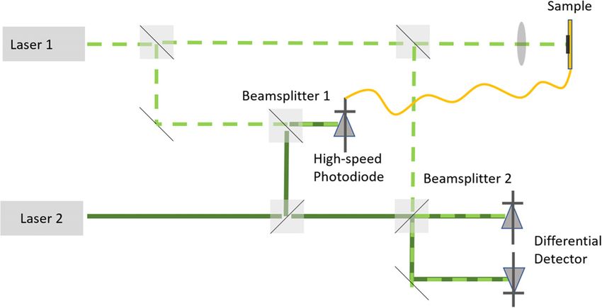
Applied Physics Letters                                                                                             ARTICLE               scitation.org/journal/apl

      5                                                                                         21
        K. Y. Camsari, R. Faria, B. M. Sutton, and S. Datta, “Stochastic p-bits for               T. Sebastian, K. Schultheiss, B. Obry, B. Hillebrands, and H. Schultheiss,
        invertible logic,” Phys. Rev. X 7, 031014 (2017).                                         “Micro-Focused Brillouin light scattering: imaging spin waves at the nano-
      6
        W. A. Borders, A. Z. Pervaiz, S. Fukami, K. Y. Camsari, H. Ohno, and S. Datta,            scale,” Front. Phys. 3, 35 (2015).
                                                                                                22
        “Integer factorization using stochastic magnetic tunnel junctions,” Nature 573,            J. C. Sankey, P. M. Braganca, A. G. F. Garcia, I. N. Krivorotov, R. A. Buhrman,
        390 (2019).                                                                                and D. C. Ralph, “Spin-transfer-driven ferromagnetic resonance of individual
      7
        M. W. Daniels, A. Madhavan, P. Talatchian, A. Mizrahi, and M. D. Stiles,                   nanomagnets,” Phys. Rev. Lett. 96, 227601 (2006).
                                                                                                23
        “Energy-efficient stochastic computing with superparamagnetic tunnel                        D. Herranz, A. Gomez-Ibarlucea, M. Sch€afers, A. Lara, G. Reiss, and F. G.
        junctions,” Phys. Rev. Appl. 13, 034016 (2020).                                            Aliev, “Low frequency noise due to magnetic inhomogeneities in submicron
      8
        M. Sharad, D. Fan, and K. Roy, “Spin-neurons: A possible path to energy-                   FeCoB/MgO/FeCoB magnetic tunnel junctions,” Appl. Phys. Lett. 99, 062511
        efficient neuromorphic computers,” J. Appl. Phys. 114, 234906 (2013).                       (2011).
      9                                                                                         24
        N. Hassan, X. Hu, L. Jiang-Wei, W. H. Brigner, O. G. Akinola, F. Garcia-                   Z. Zhang, P. C. Hammel, and P. E. Wigen, “Observation of ferromagnetic reso-
        Sanchez, M. Pasquale, C. H. Bennett, J. A. C. Incorvia, and J. S. Friedman,                nance in a microscopic sample using magnetic resonance force microscopy,”
        “Magnetic domain wall neuron with lateral inhibition,” J. Appl. Phys. 124,                 Appl. Phys. Lett. 68, 2005 (1996).
                                                                                                25
        152127 (2018).                                                                             O. Klein, G. de Loubens, V. V. Naletov, F. Boust, T. Guillet, H. Hurdequint, A.
    10
       J. Grollier, D. Querlioz, K. Y. Camsari, K. Everschor-Sitte, S. Fukami, and M.              Leksikov, A. N. Slavin, V. S. Tiberkevich, and N. Vukadinovic, “Ferromagnetic
       D. Stiles, “Neuromorphic Spintronics,” Nat. Electron. 3, 360 (2020).                        resonance force spectroscopy of individual submicron-size samples,” Phys.
    11
      C. Safranski and J. Z. Sun, “Interface moment dynamics and its contribution to               Rev. B 78, 144410 (2008).
                                                                                                26
      spin-transfer torque switching process in magnetic tunnel junctions,” Phys. Rev.             Y. Acremann, C. H. Back, M. Buess, O. Portmann, A. Vaterlaus, D. Pescia, and
      B 100, 014435 (2019).                                                                        H. Melchior, “Imaging precessional motion of the magnetization vector,”
    12
       T. Devolder, J. V. Kim, J. Swerts, S. Couet, S. Rao, W. Kim, S. Mertens, G. Kar,            Science 290, 492 (2000).
                                                                                                27
       and V. Nikitin, “Material developments and domain wall based nanosecond-                    H. T. Nembach, J. M. Shaw, C. T. Boone, and T. J. Silva, “Mode- and size-
       scale switching process in perpendicularly magnetized STT-MRAM cells                        dependent Landau-Lifshitz damping in magnetic nanostructures: evidence for
       (invited),” IEEE Trans. Magn. 54, 3400109 (2018).                                           nonlocal damping,” Phys. Rev. Lett. 110, 117201 (2013).
    13                                                                                          28
       E. R. Evarts, R. Heindl, W. H. Rippard, and M. R. Pufall, “Correlation of anom-             A. A. Tulapurkar, Y. Suzuki, A. Fukushima, H. Kubota, H. Maehara, K.
       alous write error rates and ferromagnetic resonance spectrum in spin-transfer-              Tsunekawa, D. D. Djayaprawira, N. Watanabe, and S. Yuasa, “Spin-torque
       torque-magnetic-random-access-memory devices containing in-plane free                       diode effect in magnetic tunnel junctions,” Nature 438, 339 (2005).
                                                                                                29
       layers,” Appl. Phys. Lett. 104, 212402 (2014).                                              L. Thomas, G. Jan, S. Le, S. Serrano-Guisan, Y.-J. Lee, H. Liu, J. Zhu, J. Iwata-
    14
       J. W. Lau, X. Liu, R. C. Boling, and J. M. Shaw, “Decoupling nucleation and                 Harms, R.-Y. Tong, S. Patel, V. Sundar, D. Shen, Y. Yang, R. He, J. Haq, Z.
       domain-wall propagation regimes in (Co/Pd)n multilayer nanostructures,”                     Teng, V. Lam, P. Liu, Y.-J. Wang, T. Zhong, and P.-K. Wang, “Probing mag-
       Phys. Rev. B 84, 214427 (2011).                                                             netic properties of STT-MRAM devices down to sub-20 nm using spin-torque
    15
       B. B. Maranville, R. D. McMichael, and D. W. Abraham, “Variation of thin film                FMR,” in IEEE International Electron Devices Meeting (IEDM) (2017), pp.
       edge magnetic properties with patterning process conditions in Ni80Fe20                     38.4.1–38.4.4.
                                                                                                30
       stripes,” Appl. Phys. Lett. 90, 232504 (2007).                                              M. Donahue, “OOMMF user’s guide, version 1.0,” Interagency Report No.
    16
       H. T. Nembach, J. M. Shaw, T. J. Silva, W. L. Johnson, S. A. Kim, R. D.                     NISTIR 6376 (National Institute of Standards and Technology, Gaithersburg,
       McMichael, and P. Kabos, “Effects of shape distortions and imperfections on                 MD, 1999).
                                                                                                31
       mode frequencies and collective linewidths in nanomagnets,” Phys. Rev. B 83,               N. Otsu, “A threshold selection method from gray-level histograms,” IEEE
       094427 (2011).                                                                             Trans. Syst. Man Cybern. 9, 62 (1979).
    17                                                                                          32
       M. L. Schneider, J. M. Shaw, A. B. Kos, T. Gerrits, T. J. Silva, and R. D. McMichael,       M. Dvornik, A. Vansteenkiste, and B. Van Waeyenberge, “Micromagnetic
       “Spin dynamics and damping in nanomagnets measured directly by frequency-                   modeling of anisotropic damping in magnetic nanoelements,” Phys. Rev. B 88,
       resolved magneto-optic Kerr effect,” J. Appl. Phys. 102, 103909 (2007).                     054427 (2013).
    18                                                                                          33
       Z. Ma, D. G. Seiler, and D. G. Seiler, Metrology and Diagnostic Techniques for              S. Cornelissen, L. Bianchini, A. Helmer, T. Devolder, J.-V. Kim, M. Op de
       Nanoelectronics (Jenny Stanford Publishing, 2017).                                          Beeck, W. Van Roy, L. Lagae, and C. Chappert, “Effect of patterning on the sat-
    19
       M. Kammerer, M. Weigand, M. Curcic, M. Noske, M. Sproll, A. Vansteenkiste,                  uration magnetization in MgO based nanopillars,” J. Appl. Phys. 105, 07B903
       B. Van Waeyenberge, H. Stoll, G. Woltersdorf, C. H. Back, and G. Schuetz,                   (2009).
                                                                                                34
       “Magnetic vortex core reversal by excitation of spin waves,” Nat. Commun. 2,                R. D. McMichael and B. B. Maranville, “Edge saturation fields and dynamic
       279 (2011).                                                                                 edge modes in ideal and nonideal magnetic film edges,” Phys. Rev. B 74,
    20
        S. Bonetti, R. Kukreja, Z. Chen, D. Spoddig, K. Ollefs, C. Sch€           oppner, R.       024424 (2006).
                                                                                                35
        Meckenstock, A. Ney, J. Pinto, R. Houanche, J. Frisch, J. St€ohr, H. A. D€urr, and H.      J. W. Lau, R. D. McMichael, M. A. Schofield, and Y. Zhu, “Correlation of edge
        Ohldag, “Microwave soft x-ray microscopy for nanoscale magnetization dynamics              roughness to nucleation field and nucleation field distribution in patterned per-
        in the 5–10 GHz frequency range,” Rev. Sci. Instrum. 86, 093703 (2015).                    malloy elements,” J. Appl. Phys. 102, 023916 (2007).

Appl. Phys. Lett. 118, 012408 (2021); doi: 10.1063/5.0039188                                                                                                           118, 012408-5
Published under license by AIP Publishing
You can also read