Design and Implementation of NIOS II System for Audio Application
←
→
Page content transcription
If your browser does not render page correctly, please read the page content below
IACSIT International Journal of Engineering and Technology, Vol. 5, No. 5, October 2013

      Design and Implementation of NIOS II System for Audio
                          Application
                                               S. Moslehpour, K. Jenab, and E. H. Siliveri

                                                                                    custom peripherals.
   Abstract—This project deals with the NIOS II system, which                          In SOPC Builder, the system components are routed in a
reads wave files from an SD card in real time and produces                          GUI (Graphical User Interface). The GUI is exclusive in
sound output through speakers while providing user interaction                      configuring the soft-hardware components. It is a
such as pause music, fast forward and rewind. The Altera DE2
board supports communication through the SD card. It also
                                                                                    general-purpose tool for creating systems that includes a soft
features sound recording for 10 seconds by giving a microphone                      processor apart from the Nios II processor. It also contributes
to the LINE-IN provided on the DE2 board and speakers to the                        to writing software and system simulation.
LINE-OUT. These features are realized using Altera SOPC
builder in the Altera Quartus 9.1 environment. The overall goal                       A. Core Functionalities of SOPC Builder
of this project is to explore various applications that are                                 • Describes the hardware of the system.
possible with Altera’s DE2 Board.                                                           • Performs the system generation.
                                                                                            • Performs memory mapping for initiating the
  Index Terms— DE2 board, NIOS II processor, SOPC builder,
SD card, LCD, Cyclone II 2C35 FPGA.
                                                                                               software development
                                                                                            • Produces test bench to simulate the design.
                                                                                      B. Architecture and Design of SOPC Builder
                          I. INTRODUCTION
                                                                                       Designs using SOPC Builder are generated to develop a
   Audio devices these days come in many forms of                                   top level HDL (hardware description language) file by
embedded systems and they are widely used all over the                              connecting various modules together. These various modules
world due to their compactness and ease of use. This                                are considered the building blocks for the SOPC Builder
popularity of such devices was the inspiring factor behind                          system [9]. For the connection of multiple components in the
this project [6]-[8]. There are myriad applications of these                        system, the modules use Avalon (Avalon switch interconnect)
devices such as mobile phones, portable video games etc.                            interfaces, such as memory-mapped, streaming and IRQ
   This article discusses in detail, the implementation of the                      (interrupt request).
audio application using SOPC builder, NIOS II processor
and Altera DE2 board. Given the toolset, it was a challenging                         C. SOPC Components
and a rewarding experience to have implemented this project.                           The components in SOPC Builder are referred as hardware
                                                                                    blocks of the system. They contain HDL descriptions of the
                                                                                    hardware of the components and interfaces used for the
II. SOPC (SYSTEM-ON-A-PROGRAMMABLE-CHIP) BUILDER                                    hardware. They also contain the description of the parameters
   SOPC builder is a powerful system development tools for                          that determine the operation of the components (Fig. 1).
creating systems based on processors, peripherals, interfaces                          The SOPC components are connected to the system
and memories. SOPC Builder is implemented for the purpose                           interconnect fabric using the Avalon Memory-Mapped
of generating a complete system-on-a-programmable-chip                              interface (Avalon MM) or the Avalon streaming interface
(SOPC) by consuming less time than the accustomed                                   (Avalon-ST) [4].
integration methods [4].
   Altera has SOPC Builder functionality built in Quartus II,
which accordingly connects the soft-hardware components to
construct a complete computer system that can be controlled
on any of the FPGA chips and is also capable of producing
interconnect logic automatically. It is outfitted with a library
of built-in components such as a Nios II soft processor,
memory controllers, interfaces, standard peripherals and

    Manuscript received May 28, 2013, revised June 25, 2013.
    S. Moslehpour is with the College of Engineering, Technology, and
Architecture at Hartford University, Hartford, CT, USA (e-mail:
moslehpou@hartford.edu).
    K. Jenab is with the Society of Reliability Engineering-Ottawa Chapter,
Ottawa, Ontario, Canada (e-mail: jenab@ieee.org).
    E. H. Siliveri was with the College of Engineering, Technology, and             Fig. 1. SOPC Builder with system components inside and outside the system
Architecture at Hartford University, Hartford, CT, USA (e-mail:                                                      module
siliveri@hartford.edu).

DOI: 10.7763/IJET.2013.V5.631                                                 627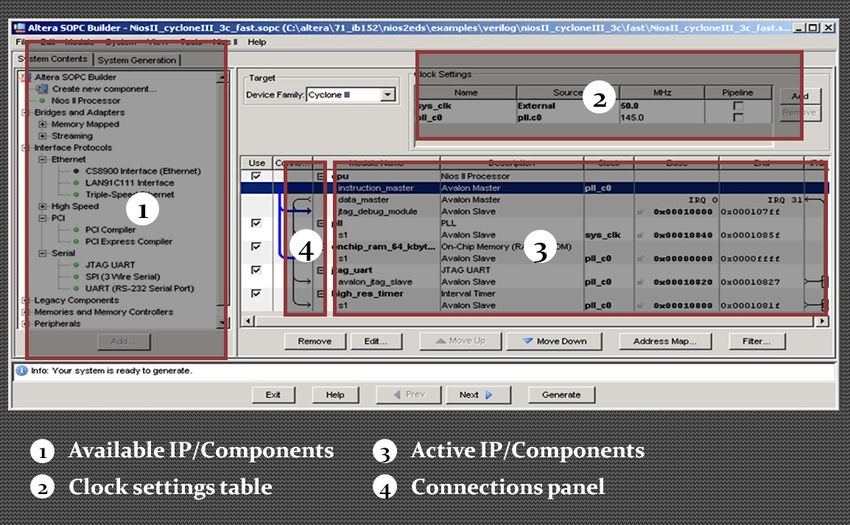
IACSIT International Journal of Engineering and Technology, Vol. 5, No. 5, October 2013

  D. Types of SOPC Components                                             F. Avalon Switch Interconnect
   SOPC Builder’s inbuilt components are                                   The Avalon Memory-Mapped (Avalon-MM) interface has
   a. Static HDL Components                                             a bandwidth of steep structure generally used for interfacing
   b. Generated HDL Components                                          the components of the system. The Avalon switch
   c. Composed HDL Components                                           interconnects uses less logic but supplies absolute flexibility.
   d. Custom Components                                                 This interconnect is a cross-connect fabric used for the
   e. Third-Party Components                                            purpose of switching and multiplexing.
   (a) Static Components: These are the components that                    The Avalon switch interconnect fabric is a combination of
accept the VHDL parameters.                                             interconnect and logic resources. It is used for stocking the
   Examples: Address widths, Data widths and FIFO depths.               Avalon memory mapped master and slaves on the
   (b) Generated Components: These are the components
                                                                        components. It is referred to a device having information
whose hardware description language file is generated based
                                                                        about connections of the entire system and its components. It
on the value of its specified parameters.
                                                                        assures that connections between the master and slaves are
   Example: A parameter that controls the number of
                                                                        routed precisely. This meets the requirements of the
interfaces.
   (c) Composed Components: These are the components                    components.
that are constructed from combinations of other components.                The interconnect fabric permits the connection of an
   (d) Custom Components: The design flow used to merge                 unlimited count of master components and slave components.
the custom components into the SOPC Builder is as follows:              These master and slave components can have a one-to-one
   1. Determine the interfaces required by the custom                   connection, a one-to-many connection, a many-to-one
components.                                                             connection, or a many-to-many connection. The system
   2. Write the logic for each custom component.                        interconnect fabric is used to support the interfaces for the
   3. Develop the custom components with the hardware                   on-chip components of the system and interfaces for the
description language files by using the component editor.               off-chip devices of the system. In this interconnect fabric,
   4. Represent the custom component in the system by an                master components and slave components with altered data
instance.                                                               widths are supported.
   (e) Third-Party Components: These components are built                  The system interconnect fabric also serves as a platform
by third parties. Components external to the SOPC Builder:              for the master and slave components running with several
For the components that interfere to external logic or off-chip         clock domains. It also supports master and slave components
devices with Avalon- compatible signals outside the SOPC                with several memory mapped ports.
Builder system, the component files describe only the                      The system implementation fabric for the Avalon-MM
interface to the external logic. The connection of signals at
                                                                        interfaces acts as a partial crossbar interconnects structure.
the top-level of SOPC Builder to pins or logic defined outside
                                                                        The partial crossbar interconnect structure is a matrix with
the system is done manually.
                                                                        multiple inputs and multiple outputs. This interconnect
  E. SOPC Design Flow                                                   structure arranges simultaneous paths between the master
   The design flow of SOPC Builder is as follows (Fig. 2)               and slave components. In the Cyclone II FPGA, routing
a. Add components by Component Editor.                                  resources and synchronous logic constitute the system
b. Initiate Simulation of the system.                                   interconnect fabric.
c. Develop the system design by adding components, IRQs
and addresses.                                                           G. Functionalities of System Interconnect Fabric
d. Start the system generation.                                            a. Decoding Address
e. Conduct system level simulation.                                        b. Multiplexing Datapath
f. Compile the system design.                                              c. Insertion of Wait State
g. Download .sof file to an Altera FPGA.                                   d. Pipelined Read Transfers
h. Perform Testing.                                                        e. Multi-master System Arbitration
                                                                           f. Burst Adapters
                                                                           g. Interrupts
                                                                           h. Reset Distribution

                                                                          H. Automated System Generation
                                                                           SOPC Builder system integration tools automatically
                                                                        perform the process of configuration of the processor
                                                                        features, hence the hardware of the design is produced that is
                                                                        used to program an Altera device. The graphical user
                                                                        interfaces (GUI) help in structuring of Nios II systems with
                                                                        multiple peripherals and memory interfaces (Fig. 3).
                                                                           After system generation, you can download the design
                    Fig. 2. SOPC Design Flow                            onto a board, and debug the software executing on the board.

                                                                  628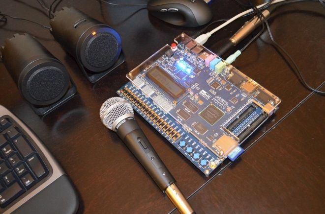
IACSIT International Journal of Engineering and Technology, Vol. 5, No. 5, October 2013

                                                                                     a. Functional units of the Nios II architecture
                                                                                     b. Fundamentals of the hardware implementation

                                                                                     B. Fundamentals of the hardware implementation
                                                                                      The hardware implementation of Nios II architecture
                                                                                   explains an instruction set. Any functional unit whose
                                                                                   hardware is implemented can be programmed in software.
                                                                                   Every hardware implementation has different objectives, for
                                                                                   example, that the size of the core should be small and must
                                                                                   yield high performance (Fig. 5). These features help the Nios
                                                                                   II architecture adjust to many different applications.
Fig. 3. SOPC Builder graphical user interfaces (GUI) of the system used in            Implementation of the processor core specifically requires
                               the project                                         any of three trade-offs: more performance or less
                                                                                   performance of a feature; inclusion of a feature in the core or
                                                                                   exclusion of a feature; and implementation of the hardware
      III. NIOS II SYSTEM ON ALTERA’S DE2 BOARD                                    and software programming of the features included in the
   The Nios II processor and many other components such as                         core.
standard peripherals and custom peripherals are used for the
formation of a total system that can be integrated into a Nios
II system on Altera’s DE2 board [3]. The process of
interfacing the Nios II processor and peripherals to the DE2
board chips is enabled on the Cyclone II FPGA chip. The
interconnection network connecting these components in the
FPGA chip is called the Avalon Switch Fabric (Fig. 4).

                                                                                                Fig. 5. Nios II Processor Core Block Diagram

            Fig. 4. Nios II system implemented on the DE2 board
                                                                                    C. Nios II Processor Core Architecture
                                                                                     The architecture of Nios II processor core consists of [3]
   The memory blocks available in the Cyclone II FPGA chip                           a. Register file
serve as the on-chip memory for the Nios II processor. These                         b. Arithmetic logic unit (ALU)
memory blocks can be connected to the Nios II processor                              c. Interface to custom instruction logic
directly with the help of the Avalon network. The Input /                            d. Exception controller
Output interfaces are used for connecting I/O devices. A                             e. Interrupt controller
JTAG UART interface is used for the purpose of providing a                           f. Instruction bus
Universal Serial Bus link between the Altera’s DE2 board                             g. Data bus
and the host computer to which the board is connected. This                          h. Memory management unit (MMU)
Universal Serial Bus link is called the USB-Blaster. The                             i. Memory protection unit (MPU)
JTAG Debug module is used by the host computer to control                            j. Cache memories
the Nios II processor, downloading programs into the                                 k. Tightly-coupled memory interfaces for instructions and
memory, starting and stopping execution. The memory chips                          data
such as SRAM and SDRAM can be connected by applicable                                l. JTAG debug module
interfaces. A hardware description language is used to define
all the Nios II system components on the Cyclone II FPGA                             D. Customizing Nios II Processor
chip.                                                                                 Altera FPGAs offer to add new features in order to
                                                                                   increase the performance of the Nios II processor. The
  A. Nios II Processor                                                             advantage of customization is elimination of unnecessary
  The Nios II processor is a configurable RISC processor                           processor features and peripherals to suite the hardware
[10]. Hardware structure includes:                                                 design in a smaller and lower-cost device.

                                                                             629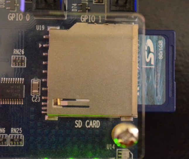
IACSIT International Journal of Engineering and Technology, Vol. 5, No. 5, October 2013
The following are the possibilities to program customized IV. SOPC BUILDER IP CORES
pins and logic resources available on the Altera DE2 board
[1]: A. Secure Data Card IP Core
a. Rearrangement of the pins on the chip is the best way to An SD card (Secure Data Card) is a data storage device [2].
reduce the design of the board. For example, address and data It is often used in digital appliances such as cameras,
pins can be moved for external SDRAM memory to cut the camcorders, MP3 players etc. It is very handy and it allows
traces of the board in short. the data stored on it to be transferred across multiple devices.
b. The use of extra pins and logic resources on the chip is The Altera DE2 board contains an SD card port. We can
independent of the processor. Extra resources supply a few connect an SD card to the FPGA-based board, and it allows
more extra gates and registers for the purpose of designing access large amount of data.
the board (Fig. 6). Also, these extra resources affect the The SD Card IP Core is a hardware circuit on the DE2
complete system. Using extra pins and logic resources on the board. It facilitates the use of an SD card. When it is included
chip, the additional peripherals for the Nios II processor can in a design and connected to the SD card port, the core detects
be implemented. We can easily access the additional an SD card when plugged into the port. This lets the circuit
peripherals from the library of SOPC Builder, which are used easily access any data stored on it.
for connecting the Nios II processor [3].
B. Functionality of SD card IP core
This IP core acts as an interface between the system and
the SD card. In the SD card IP core the signals on the left side
map to the Avalon interconnect. The Avalon interconnect
receives read and write requests from the Avalon Interface
Finite State Machine (FSM) and interprets them as command
or data requests. The SD card is configured by the commands
received, and the commands could reference various sections
of the SD card as required. The raw data stored on the SD
card is accessed by data requests. Once the finite state
machine confirms the request issued, the SD card interface
module is activated. This module communicates with the SD
card to process the request by using serial communication
protocol, and the result of the finite state machine is returned.
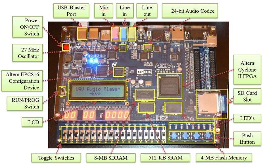
Fig. 6. Altera DE2 Board (Cyclone II 2C35 FPGA) Components and
interfaces Once the operation is complete, the result of the request is
sent by the Avalon Interface FSM through its interconnect.
E. Features of DE2 Board (Altera Cyclone II 2C35 C. Instantiating the Core in SOPC Builder
FPGA)
To be able to add the SD Card IP Core in a SOPC design, it
Following is the list of features available on the DE2 is necessary to create an instance of the core in the design. On
Board [4]: including this IP core in the SOPC design, it is very important
a. USB Blaster is inbuilt on the board mainly for to connect the card’s ports to their corresponding pins on
programming purposes and for controlling API DE2 board [2]. This can be done through the pin assignment
b. JTAG Mode and AS Mode are supported tool in the SOPC builder.
c. 8 MB (1M × 4 × 16) SDRAM
d. 1 MB Flash Memory TABLE I: PIN ASSIGNMENTS FOR SD CARD PORT ON DE1, DE2, DE3
e. SD Card Port BOARDS
f. 4 Push-buttons Pin Name DE1 DE2 DE3
g. 18 DPDT (Double Pole Double Throw) switches b_SD_cmd PIN_Y20 PIN_Y21 PIN_R10
h. 9 Green User LEDs b_SD_dat PIN_W20 PIN_AD24 PIN_P7
i. 18 Red User LEDs b_SD_dat3 PIN_U20 PIN_AC23 ‘Z’
j. 50 MHz Oscillator
o_SD_clock PIN_V20 PIN_AD25 PIN_P8
k. 27 MHz Oscillator
l. 24-bit Audio CODEC including line-in/out, and mic-in
jacks On instantiating the SD card IP core in the design, the
m.VGA DAC Avalon Interface, the reset signals are automatically
n. VGA out connector connected to the synchronous and asynchronous reset signals.
o. TV Decoder The clock input can either be set to 50 MHz or connected to
p. TV-in connector an external clock source.
q. Ethernet Controller D. Software Programming Model
r. USB Controller as Host and Slave We can build software programs to communicate with the
s. RS-232 Transceiver and 9-pin connector SD card directly. This can be done with the help of
t. Mouse and keyboard connectors (PS/2) memory-mapped registers and a memory-mapped buffer, or
u. IrDA transceiver using HAL drivers.
v. 2 x 40-pin Expansion Headers
630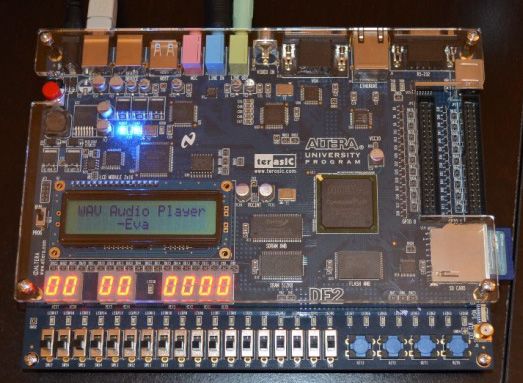
IACSIT International Journal of Engineering and Technology, Vol. 5, No. 5, October 2013

  E. Direct SD Card Communication using                                 table marking showing the position of files in the system (Fig.
  Memory-Mapped Registers                                               8). This system partitions the whole memory into blocks of
   Using the memory-mapped registers, information can be                data, each block consisting of 512 bytes and the smallest
exchanged between the SD card and the SOPC system. The                  possible data is 16 bit long [5].
SD card interface status can be read programmatically
through these registers. Read/Write commands can also be
sent using the same mechanism. This allows reading, writing
and erasing blocks of data available on the SD card.
  F. Hardware Abstraction Layer Device Driver
   HAL device drivers facilitates convenient access to all the
data store on the SD card. HAL drivers can act as a FAT (File
Allocation Table) reader and FAT writer and thus make it
possible to access SD card data. This requires the data on the
SD card to be saved in FAT16 format. Other file systems
such as FAT12, FAT32 and NTFS are not compatible with
the DE2 board.
  G. Formatting the SD Card in FAT16 format
   Data is stored in several clusters. These clusters are
identified by an ID that ranges from 2 through 65520. Files                           Fig. 8. SD card Controller on DE2 Board
stored on the SD card, in the FAT16 format, occupy several
clusters depending on the size of the file. The SD card IP core           B. Serial Peripheral Interface (SPI) mode of
we use works only with FAT16 because it requires at least                 communication
4087 clusters and at most 65520 clusters so that they can be               SPI is a synchronous serial data link that functions with a
represented by 16-bit IDs.                                              single master and multiple slaves (at least one). In this design
                                                                        we use the SPI mode of communication to access the SD card
                                                                        (Fig. 9). Data transfers are carried out using one bit. This
               V. PROJECT IMPLEMENTATION                                allows for an easy and simple interface design [1].
  This project deals with a NIOS II system that reads the
wave files from the SD card in real time and produces sound
output through speakers while providing user interaction
such as pause music, fast forward and rewind. For
implementing this system, the following are required:
    a. SD card Controller
    b. SPI mode of communication
    c. Audio codec
    d. SOPC Builder
    e. Nios II processor

  A. SD card Controller
  DE2 board comes with an SD card port which can be
                                                                                               Fig. 9. SPI Interface
connected to an SD card (Fig. 7). An SD card is one of the
memories used in this project.                                            The pins used in SPI are
                                                                           a. SD_CLK
                                                                           b. SD_DATA
                                                                           c. SD_CMD

                                                                        SD_CLK: Used to control the SD card clock speed
                                                                        SD_CMD: Used to send commands to the SD card. CMD
                                                                        constitutes standard SD card commands, and ACMD
                                                                        constitutes specific commands.
                                                                        SD_DATA: Used for data transfer.

                                                                          C. Audio Codec (Wolfson Wm8731)
                         Fig. 7. SD card
                                                                          An audio codec is nothing but a device that performs
  For the SD card to be detected, it should be formatted with           encoding of analog audio signal to a digital signal. It also
FAT 16 file format. The FAT (File Allocation Table) is a                decodes a digital signal to an analog audio signal. It
                                                                        constitutes an ADC and DAC, which are clocked by the same

                                                                  631
IACSIT International Journal of Engineering and Technology, Vol. 5, No. 5, October 2013

clock input. In order to generate sound using the board, the                c. Nios II / e: This is an "economy" version that needs
audio data is transferred from the SD card to the analog line                   least possible FPGA resources. This limits the
out port of the DE2 board. In this project, we use a 24-bit                     feature set to bare minimum functionality (Fig. 11).
sigma-delta audio codec called as Wolfson WM8731 [3].
Modules used in the Audio Codec system are:
    a. FIFO module
    b. I2C interface unit
    c. PPL module

   FIFO module is nothing but a buffer with a width of
256x16 bits. It connects the Nios and Digital to Analog
Converter (DAC). The data flow of the codec is controlled by
the I2C interface unit. PPL module produces an 18.4 MHz
clock frequency. The .wav file is sampled at 48 KHz.
                                                                                        Fig. 11. NIOS II core configurations
  D. SOPC Builder
  All the components used in this project are connected                   F. Nios II Code Flow
using the SOPC builder. The SPI interface pins are the PIO’s
                                                                           The Nios II processor looks for the SD card if it is inserted
used for communication with the DE2 board (Fig. 10).
                                                                        into its slot when the board is switched on. The SD card is
                                                                        initialized as soon as it is inserted and the files are detected
                                                                        and the file directories are listed using FAT 16 (Fig. 12). FAT
                                                                        16 is used to search any media content available on the card
                                                                        which is inserted in the SD card slot. The media files are
                                                                        stored as file type: .WAV. The file names are then printed on
                                                                        the LCD character display of the DE2 board, and the user can
                                                                        select the desired song. Once the user selects a song, he can
                                                                        play the selected song from the beginning. Songs are played
                                                                        continuously when the SW[0] switch is turned on.

                     Fig. 10. SOPC Builder

  E. Nios II Processor
   The Nios II processor is used to implement all the
functions of this project. The Nios II processor is based on a
Reduced Instruction Set Computer (RISC) architecture. The
                                                                                          Fig 12 NIOS II Code Flow Chart
general purpose register’s operands are used to perform
arithmetic and logic operations.
                                                                           To browse through the available songs in the playlist,
   In the Nios II architecture, we have two separate buses for
                                                                        key-2 and key-3 of the board are used and a specific song can
sending instructions and transferring data. This architecture
                                                                        be selected. The name of the current song is displayed on the
is also popularly known as Harvard architecture. It has 32-bit
                                                                        LCD screen for browsing and for selecting the song. Once
registers and 32-bit word length as well.
                                                                        browsing through the playlist is done by the user from the
There are three available configurations in which the Nios II
                                                                        directory and a particular song is selected, Key-1 is pressed to
processor can be implemented. They are as follows:
                                                                        select the song, which is indicated on the LCD screen. Once
    a. Nios II / f: This is a "fast" version optimized for high         the song is selected, the digital data is read from the card and
        performance.                                                    sent to the FIFO buffer. Switch SW-4 is used to fast-forward,
    b. Nios II / s: This is a "standard" version that                   reverse play is enabled using SW-5, and the song can be
        optimizes the resources available in the FPGA                   paused with SW-6. On completion of the song, the LCD
        device. This trades off resource optimization with              displays the main menu on the board. SW-17 is used to reset
        performance.                                                    the board.

                                                                  632
IACSIT International Journal of Engineering and Technology, Vol. 5, No. 5, October 2013

                  VI. RESULTS AND DISCUSSION
   This project reads the wave files from the SD card and
produces sound output through speakers while providing
user interaction such as play, pause, and reverse play at
various speeds as shown in Fig. 13. The SD card is primarily
used as the source of music files in this project. It also
features sound recording by giving the microphone to the
LINE-IN provided on the DE2 board and speakers to the                                                              Paused audio
LINE-OUT. Once the sound is recorded, there are several
playback options such as pause, fast forward and rewind.
These features are achieved using SOPC Builder tool
provided by Altera, and programming of the DE2 board is
done by Nios II Eclipse.

                                                                                                             Reverse playback of audio
                                                                                          Fig. 13. Demonstration of NIOS II System on DE2 Board for Audio
                                                                                                                     Application

                                                                                                                  REFERENCES
                                                                                    [1]  Altera Audio/Video Configuration Core for DE2-Series Boards. (July
                                                                                         2010).                       [Online].                       Available:
                                                                                         ftp://ftp.altera.com/up/pub/Altera_Material/10.1/Universiy_Program_I
                                                                                         P_Cores/Audio_Video/Audio_and_Video_Config.pdf
                                                                                    [2] SD card IP Core. Altera University Program Secure Data Card IP Core.
                                                                                         (March               2009).             [Online].            Available:
The project setup includes speakers, mic and the DE2 board connected to the              ftp://ftp.altera.com/up/pub/University_Program_IP_Cores/90/SD_Car
                                 computer                                                d_Interface_for_SOPC_Builder.pdf (accessed September 19 -2012)
                                                                                    [3] Wolfson Electronics. (2004, April). Portable Internet Audio CODEC
                                                                                         with Headphone Driver and Programmable Sample Rates. (WM8731
                                                                                         Rev3.4). [Online]. Available: https://instruct1.cit.cornell.edu/courses
                                                                                         /ece576/DE2_Datasheets/Audio%20CODEC/WM8731_WM8731L.p
                                                                                         df (accessed October 22-2012)
                                                                                    [4] Altera SOPC Builder User Guide. (2010, December). [Online].
                                                                                         Available: http://www.altera.com/literature/ug/ug_SOPC_builder.pdf
                                                                                    [5] Altera Embedded Peripherals IP Guide. (2011, June). [Online].
                                                                                         Available: http://www.altera.com/literature/ug/ug_embedded_ip.pdf
                                                                                    [6] S. Moslehpour, K. Jenab and B.S. Pabla, “Implementing a soft core
                                                                                         NIOS II processor for VGA application,” International Journal of
                                                                                         Engineering Research and Innovation. vol.4, no.2, pp. 12-26, 2012.
                                                                                    [7] S. Moslehpour, K. Jenab and S. Valiveti, “GPS time reception using
                                                                                         Altera SOPC builder and Nios II: Application in train positioning,”
                                                                                         International Journal of Industrial Engineering and Production
                                                                                         Research, vol.23, no.1, pp. 13-21, 2012.
                                                                                    [8] S. Moslehpour, K. Jenab and B. K. Matcha, Design of the Nios II
                                                                                         System for the Playing of Wave Files on an Altera DE2 Board, 2012.
                                                                                    [9] J. O. Hamblen and T. S. Hall, “Using system on a programmable chip
                 Start screen of the project on DE2 board                                technology to design embedded systems,” IJCA, vol.13, no.3, pp. 1-11,
                                                                                         2006.
                                                                                    [10] My First NIOS II Software, Altera Corporation based on Altera
                                                                                         Complete Design Suite Vrsion9.1,. January 2010. [Online]. Available:
                                                                                         http://www.altera.com/literature/tt/tt_my_first_nios_sw.pdf

                   Recording audio through microphone                                                     Saeid Moslehpour is an associate professor and
                                                                                                          department chair in the Electrical and Computer
                                                                                                          Engineering Department in the College of
                                                                                                          Engineering, Technology, and Architecture at the
                                                                                                          University of Hartford. He holds Ph.D. (1993) from
                                                                                                          Iowa State University and Bachelor of Science
                                                                                                          (1989) and Master of Science (1990) degrees from
                                                                                                          University of Central Missouri. His research
                                                                                                          interests include logic design, CPLDs, FPGAs,
                                                                                    Embedded electronic system testing and distance learning.
    Playing at 1x speed. 4x and 8x playback speeds are also supported

                                                                              633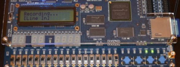
IACSIT International Journal of Engineering and Technology, Vol. 5, No. 5, October 2013

                       Kouroush Jenab is a senior member of IEEE who                      Evangeline Harica Siliveri received the bachelor
                       received the B.Sc. degree from the IE Department at                degree of engineering in electronics and
                       Isfahan University of Technology (1989), the M.Sc.                 communications from JNTU College of Engineering,
                       degree from the IE Department at Tehran Polytechnic                India, in May 2009. She received her Master’s degree in
                       (1992), and the Ph.D. degree from the Department of                Electrical Engineering at the University of Hartford in
                       Mechanical Engineering at the University of Ottawa                 2013.
                       (2005). He served as a senior engineer/manager in
                       auto, and high-tech industries for 18 years. He joined
                       the National Research Council Canada as a research
officer where he participated in several international research projects. In
2006, he joined the Department of Mechanical and Industrial Engineering at
Ryerson University, Toronto, as an assistant professor. Currently, Dr. Jenab
is education chair of the Society of Reliability Engineering (SRE)-Ottawa
Chapter. He has published over 81 papers in international scientific journals
and conferences, edited a special issue on Applied Computational
Techniques in Engineering and Technology for the International Journal of
Industrial Engineering Computations, and produced over 29 technical
reports.

                                                                                634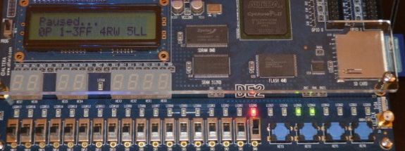

You can also read