Embedded system for GNU/Taler - Designing an embedded system for cashless payment on a vending machine
←
→
Page content transcription
If your browser does not render page correctly, please read the page content below
Embedded system for GNU/Taler
 Designing an embedded system for cashless payment on a
                   vending machine

                                          Bachelor’s Thesis

Field of Studies:   Mikro- und Medizintechnik
Course:             Embedded systems
Author:             Dominik Wenger
Supervisors:        Prof. Andreas Habegger, Prof. Dr. Christian Grothoff
Expert:             Rico Zoss
Date:               July 28, 2020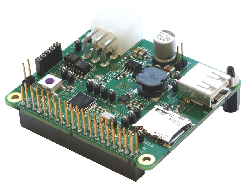
Berner Fachhochschule                                   0                              Mikro- und Medizintechnik

ABSTRACT

Digital wallet payment services are expected to account for 47 % of all E-Commerce and 28 % of all point of sale
payment methods by 2022 [1]. Unfortunately, some people have concerns about their privacy by using such digital
wallet applications, since most of the providers are big tech companies with unclear intentions.

A new participant in this global market will be GNU/Taler. It is a digital wallet service, that wants to provide a
fast and easy payment system which ensures the user’s privacy.

During this thesis, an embedded system shall be developed to allow the use of GNU/Taler for mobile payments
in vending machines.

The fundamental knowledge about vending machines has been gathered and a hardware specification book was
written. After the elaboration of different concepts, it was decided to develop a vending machine interface gateway
for a Raspberry Pi and as a further step an embedded platform, where the system shall become more tailored
and thus more compact. The gateway board was designed, manufactured and tested. Up to a few design issues,
the gateway fulfills the desired requirements. The further developed embedded platform is not manufactured yet.
The schematics have been developed and the components are selected. An outstanding process is the final board
design.

After this thesis, the development of the platform will be continued. During the next year, all coffee-vending
machines at the Berner Fachhochschule shall be equipped with the embedded platform to enable GNU/Taler
payments.

Author: Dominik Wenger                     Last change: July 28, 2020                                  Page i of ii
Berner Fachhochschule                                                          0                                                                   Mikro- und Medizintechnik

TABLE OF CONTENTS

I.    Preliminary Study                                                                                                                                                                            1
1. Introduction                                                                                                                                                                                     2
   1.1. About GNU/Taler . . . . . . . . . . . . . . . . . . . . . . . . . . . . . . . . . . . . . . . . . . .                                                                                       3
   1.2. About vending machines . . . . . . . . . . . . . . . . . . . . . . . . . . . . . . . . . . . . . . .                                                                                        4

2. Conceptioning                                                                                               10
   2.1. MDB/ICP converter module . . . . . . . . . . . . . . . . . . . . . . . . . . . . . . . . . . . . . 11
   2.2. Taler application module . . . . . . . . . . . . . . . . . . . . . . . . . . . . . . . . . . . . . . . 17

3. Prototyping                                                                                                20
   3.1. STM32 software validation . . . . . . . . . . . . . . . . . . . . . . . . . . . . . . . . . . . . . . 21

II. Thesis                                                                                                                                                                                         25
4. Introduction                                                                                                                                                                                    26

5. MDB/ICP Gateway                                                                                                                                                                                 27
   5.1. Specification Sheet . .    .   .   .   .   .   .   .   .   .   .   .   .   .   .   .   .   .   .   .   .   .   .   .   .   .   .   .   .   .   .   .   .   .   .   .   .   .   .   .   .   28
   5.2. Hardware Development       .   .   .   .   .   .   .   .   .   .   .   .   .   .   .   .   .   .   .   .   .   .   .   .   .   .   .   .   .   .   .   .   .   .   .   .   .   .   .   .   29
   5.3. Hardware Testing . . .     .   .   .   .   .   .   .   .   .   .   .   .   .   .   .   .   .   .   .   .   .   .   .   .   .   .   .   .   .   .   .   .   .   .   .   .   .   .   .   .   40
   5.4. Conclusion . . . . . . .   .   .   .   .   .   .   .   .   .   .   .   .   .   .   .   .   .   .   .   .   .   .   .   .   .   .   .   .   .   .   .   .   .   .   .   .   .   .   .   .   48

6. Embedded Platform                                                                                             49
   6.1. Specification Sheet . . . . . . . . . . . . . . . . . . . . . . . . . . . . . . . . . . . . . . . . . . 50
   6.2. Hardware development . . . . . . . . . . . . . . . . . . . . . . . . . . . . . . . . . . . . . . . . 51
   6.3. Conclusion . . . . . . . . . . . . . . . . . . . . . . . . . . . . . . . . . . . . . . . . . . . . . . . 66

7. Conclusion                                                                                                                                                                                      67

Bibliography                                                                                                                                                                                       68

Appendix                                                                                                                                                                                            1
     A.   Declaration of Autorship . . . . . .                 . . . . . .             .   .   .   .   .   .   .   .   .   .   .   .   .   .   .   .   .   .   .   .   .   .   .   .   .   .   .    1
     B.   Working journal . . . . . . . . . . .                . . . . . .             .   .   .   .   .   .   .   .   .   .   .   .   .   .   .   .   .   .   .   .   .   .   .   .   .   .   .    1
     C.   MDB/ICP Gateway Schematic . . .                      . . . . . .             .   .   .   .   .   .   .   .   .   .   .   .   .   .   .   .   .   .   .   .   .   .   .   .   .   .   .    1
     D.   Embedded Taler MDB/ICP Platform                      Schematic               .   .   .   .   .   .   .   .   .   .   .   .   .   .   .   .   .   .   .   .   .   .   .   .   .   .   .    1

Author: Dominik Wenger                                 Last change: July 28, 2020                                                                                                  Page ii of ii
Berner Fachhochschule 0 Mikro- und Medizintechnik
Part I.
Preliminary Study
Author: Dominik Wenger Last change: July 28, 2020 Page 1 of 70Berner Fachhochschule 1 Mikro- und Medizintechnik 1. Introduction In an increasingly digitized society, money in form of notes and coins is becoming less and less important. The role of cash got degraded by credit- and debit cards in the last few decades. But these cards were only forerunners to prepare the society for the future. A completely cashless world. In the past decade, smartphones became a very central device in most peoples lifes. Mobile banking and mobile payment applications have become very popular and payment systems like Apple pay, Android pay, Samsung pay, Amazon pay, Paypal, Alipay, Libra have generated a lot of attention. The advantages of such mobile payment applications seem obvious. In modern civilizations with comprehensive mobile internet there is simply no need for cash anymore. But there are concerns about mobile payment applications. If all my transactions are handled by an application on my smartphone, what will happen with the gathered information about my consumer behavior? If you look closely at the above listed payment applications, you can see that they are all founded by tech giants. Cashless payment generate a lot of detailed data about a users’ consumer behavior what can be of high interest for some parties. By allowing big tech companies to act as payment providers, the economic sovereignty is in danger and every users privacy too [2]. Unfortunately, there is currently no payment system on the market which guarantees privacy to its users. But there is one to come and it is named Taler. Taler was founded in 2014 and is part of the GNU-Project, which is engaged to provide free software1 to society. Taler is currently only available for demo usage in online transactions. But this will change. As part of this thesis, an embedded system for a vending machine shall be designed which enables the use of Taler in such devices. In advance to this thesis, a prototype based on a Raspberry Pi was developed by Dominik Hofer and Marco Boss. This prototype was presented at the famous 36C3 [5] and was even shown at the WEF in 2020. The now further developed system shall fulfill industry standards and should be able to be produced in higher quantities. Additionally, it is a personal goal to use mostly free software (or at least open-source) tools for the development of this system to mesh with the GNU philosophy. 1 Software that respects the users’ freedom. Official definition Author: Dominik Wenger Last change: July 28, 2020 Page 2 of 70
Berner Fachhochschule                     1 1.1. ABOUT GNU/TALER                       Mikro- und Medizintechnik

1.1. About GNU/Taler

Taler stands for Taxable Anonymous Libre Economic Reserves and is a free software based microtransaction
payment software. The project is led by Christian Grothoff and Florian Dold [6].

The goal of the software is to provide a payment system that makes privacy-friendly online transactions fast and
easy [3]. It is set up in such way that everybody can make a Taler account by simply registering himself with a
username and a password. There is no proof of identity necessary. This means that literally everybody is able to
participate the monetary system.

                                wire transfer                     wire transfer

                                                         make/
                                                        wire transfers

                               Figure 1.1.: Simplified Taler system architecture [7]

After the registration, the Taler user is able to advise his bank to send money to his Taler wallet. This transfer
is made trough the Taler exchange, which anonymizes the cash flow. The money that the user receives can be
found in the wallet. It has the same currency as specified in the bank transfer.

From now on, the user can perform payments and acts thereby fully anonymous to its merchants or to its bank.
Since the amount of money in this wallet is anonymized, there is consequently also no way of refunding the money
in case of theft or loss of user data.

If a payment is made, the merchant receives the money coming directly from the user’s wallet. An automatic
system becomes active and informs the government, that a transaction has been observed. There is a minimal
amount of information gathered about this transaction to ensure that the merchant cannot evade taxes.

Through the Taler exchange, the merchant can transfer its earned money back to its preferred bank.

This example is very simplified. For a more detailed insight into the Taler project, it is recommended to visit the
website 2 .

 2 www.taler.net

Author: Dominik Wenger                     Last change: July 28, 2020                                Page 3 of 70
Berner Fachhochschule 1 1.2. ABOUT VENDING MACHINES Mikro- und Medizintechnik
1.2. About vending machines
In order to design an embedded system, which shall interact with a vending machine, it is very important to get
familiar with the vending machine’s structure and communication interface.
Fortunately, every vending machine’s communication protocol is standardized by a consortium of the NAMA
(National Automatic Merchandising Association), the EVA (European Vending Association) and the EVMMA
(European Vending Machine Manufacturers Association). This protocol standard is called MDB/ICP, which
stands for Multi Drop Bus / Internal Communication Protocol [8].
NOTE: The following remarks about the MDB/ICP protocol shall be interpreted as an introduction into the thematic to the reader.
The most important conceptual compositions about the interface are explained in order to get the necessary understanding about
cashless devices in vending machines. However, some details are not (or not fully) covered.
A vending machine across this standard consists of a Vending Machine Controller (VMC) which is connected to up
to 32 slaves. Every slave represents a physical device such as coin changers, coin validators and of course cashless
devices. Each peripheral type has its defined address, its own instruction set and a specified state machine. The
peripherals are connected in serial with the VMC and are using a multidrop-bus interface.
Generally, the master (VMC) checks every slave periodically for activity. This periodical check is called polling
and will happen every 25 −200 ms. A peripheral has three different possibilities about how to answer to a master
poll. They can either answer with an acknowledge signal (ACK) or they can answer with specific process data in
order to initiate an interaction with the VMC. If the master’s message integrity is not validated, the slave can
also answer with an non-acknowledge signal (NAK). When the peripheral does not respond in a particular time,
the VMC will automatically interpret this silence as a NAK. Every communication will be initiated by the VMC.
The peripheral is not allowed to start an interaction by itself. This must always be done subsequently to a poll
command.
If the peripheral sends data to the VMC, it will receive an ACK/NAK in return. The master also has a third option,
the retransmit signal (RET). This option will force an immediate retransmission of the slave’s previous sent data.
1.2.1. Communication
On the lowest layer, the communication is done by using a 9 bit UART interface with eight data bits, one mode
bit and one stop bit:
Figure 1.2.: UART-Frame of an MDB/ICP message byte
The maximum message length in MDB/ICP amounts 36 of such frames (including a checksum- and address byte).
This means that there can be up to 34 bytes of effective data in one message block. The MODE bit is introduced
to distinguish between different types of data. This is urgently necessary since all bus participants are connected
in serial with one single transmit- and receive-line. Hence, this special bit is used for two different purposes.
I Master to slave transmission: The master has the ability to send data to a specific slave. This is done by
sending the address of this slave in the first message frame. By setting the MODE bit to ’1’, he empowers
Author: Dominik Wenger Last change: July 28, 2020 Page 4 of 70Berner Fachhochschule 1 1.2. ABOUT VENDING MACHINES Mikro- und Medizintechnik
the slaves to interpret the data in this specific frame as an address. From this point on, only the addressed
slave has to listen actively to the following data.
I Slave to master transmission: Slaves do not need to send the address-byte, since they are only able to
talk to the master. Even if all other slaves could technically read this information too, it is not intended
to allow such communications 3 . In this case, the MODE bit is used to signalize the last message frame
of an outgoing communication. This end-token is necessary because there can be a lot of traffic on the
master-receive-line, since all slaves are communicating through this single wire.
At the end of each message block, a checksum-byte is added to protect against transmission-errors. However,
there are three cases where no checksum-byte has to be calculated:
I The master/slave sends an ACK signal
I The master/slave sends a NAK signal
I The master sends a RET signal
The data for the checksum-byte is obtained by a simple addition of all message bytes (except of the checksum
itself, naturally). If the calculated checksum is too big to get stored in one byte, it is truncated. The device,
which receives the message, will do the same calculations. If the checksum differs from the received one, there is
probably a transmission error. The device should signalize this error by answering with NAK.
NOTE:This is only a fictitious example. There is no such slave and consequently no such slave data specified in the standard.
The following example shows a minimal master to slave message block:
Figure 1.3.: Minimal master to slave MDB/ICP message block
In the figure above, it should be clearly visible how the MODE bit is used to address the slave, which listens to
0x01. The following data byte contains specific instructions to this slave which are specified in the standard.
There could, as previously mentioned, even be more data bytes in the message block. At the end of the transmit,
the master calculates the checksum by adding both data values (0x01 + 0x96 = 0x97). If the checksum
increases to a number bigger than representable in one byte, it gets truncated. As an example, a checksum of
0x2F6 gets truncated to 0xF6.
Since there is no unique end-token specified to signalize the end of a master message, the slave has to detect it
through a timeout measurement. Actually, there are a few time constraints specified to ensure safe communication.
This will be discussed later.
3 Thereis a File Transport Layer (FTL), which allows communications between peripherals. The VMC will act as a network manager
to enable the communication between the two participants. However, this feature is intended for i.e. Loading system parameters
and not for standard communication. The FTL will therefore not be covered furthermore in this document.
Author: Dominik Wenger Last change: July 28, 2020 Page 5 of 70Berner Fachhochschule 1 1.2. ABOUT VENDING MACHINES Mikro- und Medizintechnik
A possible answer of the slave could look like this:
Figure 1.4.: Minimal slave to master MDB/ICP message block
Note that the slave’s idle voltage level is at 5 V, whereas the master’s is at 0 V. In contrast to the master, the
slave does not have to set the VMC’s address in order to send a message, since the VMC is the only participant
which actually listens on this wire. The MODE bit is set by the slave at the last transmitted message frame, in this
case the checksum byte. There is also the potential to send more data in one message block as specified by the
maximal block length. If the slave has no data to send, it could answer the master’s request with the ACK signal.
The checksum byte could therefore be omitted. When the checksum validation of the master request fails, the
slave will answer with a NAK signal.
As already mentioned, there are a few time constraints specified by the standard. Such time specifications are very
important and must be followed strictly by every developer. The specified constraints are presented graphically
to get a clear view.
Figure 1.5.: MDB/ICP timing constraints
Such timing properties have to be specified in every bus protocol, in order to allow a proper communication.
Especially for larger scale projects where devices from multiple manufacturers should be able to intercommunicate.
The various constraints are explained a bit closer:
I tinter−byte
Specifies the maximal allowed time between two message frames inside a message block. Slaves use this
value as timeout to detect message ends on the master line.
I tresponse
One of the most important constrains for peripheral developers. If the slave is not able to answer to a
master request in this specific amount of time, communication will be impossible. After this amount of
time, the VMC automatically interprets the absence of an answer as NAK.
I tbreak
The master can force all slaves to reset themselves by pulling the line up for this amount of time.
I tsetup
After a reset, the master has to wait for at least this long before sending new requests. This allows the
devices to return to their power on reset (POR) state and getting ready for new instructions.
The now gathered information about the bus communication level explains how the data is transferred in this
environment.
Author: Dominik Wenger Last change: July 28, 2020 Page 6 of 70Berner Fachhochschule 1 1.2. ABOUT VENDING MACHINES Mikro- und Medizintechnik
1.2.2. Cashless Devices
In this project, the Taler application will be implemented as a cashless device. The cashless device is a standard
vending machine peripheral specified by MDB/ICP. There are two addresses reserved for vending machines to
provide i.e. simultaneous mobile and credit card payment.
The functionality of most vending machine peripherals is specified by MDB/ICP. This functionality was changed/ex-
tended over different protocol versions. To distinguish between the different functionalities of the peripherals, one
introduced levels and options. Levels were established to indicate major changes on the instruction set, whereas
options are used to go further than the standard.
The master has to ensure that he only sends commands to it’s peripherals that are supported by them. In order to
do this, he has to determine each peripheral’s level before starting any interaction. The same applies for a cashless
device. It has to gather the information about the VMC’s level before any payment interaction. Generally, it is
recommended that new products are supporting all device-levels.
Cashless devices are specified for the following levels and options:
NOTE: This information is based on the MDB/ICP protocol standard 4.2.
Level Options Description
below Supports standard commands and Expansion ID command. Readers do not have revalu-
ation capability
b0* Reader is capable of restoring funds to card
1 b1* Reader is multivend capable
b2* Reader has a display available
b3* Reader supports VEND-CASH SALE command
*bits in the SETUP-Config command
2 above Supports Revalue, Time /Date, Read User File (obsolete), and Write User File (obsolete)
commands
above & Supports expansion ID command with options and optionally supports commands for
below features below (bits in the Level 3 Expansion ID command)
b0** File Transport Layer (FTL)
b1** 16 or 32 Bit Monetary Format
3 b2** Multi Currency / Multi Lingual
b3** Negative Vend
b4** Data Entry
b5** Always Idle Session
**bits in the Level 3 Expansion ID command
Table 1.1.: Levels and options of a cashless device [8]
The cashless device for this project will be a level 3 peripheral. It’s state machine is structured like this:
Author: Dominik Wenger Last change: July 28, 2020 Page 7 of 70Berner Fachhochschule 1 1.2. ABOUT VENDING MACHINES Mikro- und Medizintechnik
Figure 1.6.: FSM of a cashless device according to MDB/ICP
I Inactive:
This is the cashless device’s initial state after a power-up or a reset. The device will answer with the JUST
RESET command to a master poll in order to start a configuration exchange. During this exchange, the
master sends it’s configuration data (i.e. It’s level) to the peripheral. The peripheral will answer with his
own configuration data. After a few data exchanges, the VMC will enable the cashless devices options (if
possible). The reader is now initialized and will automatically enter the Disabled state.
I Disabled:
While the Disabled state is active, the device is not available for payments. It will proceed to the next state
after receiving the READER ENABLE command.
I Enabled:
The device is now ready for transactions. It proceeds to the next state if a valid payment media is read.
The cashless device will then inform the VMC with a BEGIN SESSION command at the next poll and go
further to the next state. However, not every payment method can read a payment media (i.e. payments
per QR-Code for the Taler project). For such reasons, there is also an optional feature (Level 3) to be in
Always idle mode. This optional mode allows the cashless device to start a vending process directly from
the Enabled state.
I Session Idle:
A session with a valid payment media has started. If the cashless device is multi currency capable, the
currency type will be set at the begin of this state. The VMC can initiate a payment process with VEND
REQUEST, REVALUE REQUEST, NEGATIVE VEND REQUEST. Each of these processes will lead auto-
matically back into this state. If the VMC sends the SESSION COMPLETE command, the cashless device
will respond with END SESSION and returns to the Enabled state.
I Vend:
The customer has entered a valid item number and now wants to pay. The item number and price is
transmitted with the VEND REQUEST command. It is now up to the cashless device to handle the purchase.
The VMC will poll the device until it has received a VEND APPROVED / VEND DENIED signal. During this
vending process, the cashless device is allowed to give no answer to the VMC polls at all for a non-response
time, which is defined by the cashless device itself. Everytime the device will send an ACK signal to a
master poll, the non-response timer is restarted. If the cashless device has approved the vend, the machine
will try to hand over the desired item. After a successful product delivery, the VMC will inform the device
with a VEND SUCCESS which leads to a fallback into the Always Idle state. If the VMC responds with
VEND FAILURE (i.e. The product could not be released), it is up to the cashless device to handle the
Author: Dominik Wenger Last change: July 28, 2020 Page 8 of 70Berner Fachhochschule 1 1.2. ABOUT VENDING MACHINES Mikro- und Medizintechnik
refund session. The customer can also abort a vend session by pressing the coin mechanism escrow button.
The VMC will then send a VEND CANCEL request, which will lead to a VEND DENIED response from the
cashless device.
I Revalue:
This session is entered because some coins or bills were accepted by the machine or a balance is left after
a vend. The revalue amount is also appended to the REVALUE REQUEST command. The cashless device
can define a revalue amount limit, which will not be exceeded by the VMC. This limit amount shall be
requested by the VMC at the beginning of the Session Idle state. The device will respond with a REVALUE
APPROVED / REVALUE DENIED and fall back into the Session Idle state.
I Negative Vend:
This vend session is similar to the normal vend state except that the in the NEGATIVE VEND REQUEST
requested amount of money will be transacted to the customer. Such transactions are used for can- or
bottle-return machines. However, the VMC has to ensure that the items are checked and not longer
accessible to the user in order to prevent fraud. This vending session is also an optional level 3 device
feature and does not have to be available.
In general, the cashless device does not need to immediately send process data to a corresponding VMC request.
If the data cannot be gathered during the specified response time of 5 ms, the cashless device can also respond
with an ACK signal or even with no signal at all until the application’s maximum response time has passed over.
This response time can be defined by the cashless device developer itself. A default response time is specified
with 5 s.
If the VMC sends a command, that does not correspond to the current state of the state machine, it will answer
with COMMAND OUT OF SEQUENCE. The VMC will then issue a reset of the cashless device.
If the VMC has a display, the cashless device can optionally request it for displaying data. Information about
whether a display is available and about the display size is exchanged in the Inactive state.
Author: Dominik Wenger Last change: July 28, 2020 Page 9 of 70Berner Fachhochschule 2 Mikro- und Medizintechnik 2. Conceptioning Since the basic knowledge about the system’s environment was aquired in the previous part, one is now able to specify the required system characteristics. This first conceptioning part is primarily focussed on the definition of the embedded system’s hardware. The embedded system will therefore be divided into two parts; A MDB/ICP converter module and a Taler application module. This division is made, since both modules have different functionalities and should work independently from each other. A specification book for each module will support a systematic elaboration of different concepts. The comparison of each concept shall lead to a comprehensible decision. Author: Dominik Wenger Last change: July 28, 2020 Page 10 of 70
Berner Fachhochschule             2 2.1. MDB/ICP CONVERTER MODULE                    Mikro- und Medizintechnik

2.1. MDB/ICP converter module

The converter module will provide the communication interface to the vending machine controller. A vending
machine peripheral is connected to the circuit through a standardized 6-Pin connector. There are two pins for the
data transmission and reception (5 V/0 V). A third pin provides the data line’s reference ground. Additionally,
there are two pins available, which provide a 34 V/0 V rated power supply from the VMC. The remaining pin is
not connected.

The module must at least provide a voltage converter and a computing unit, which provides the necessary
communication interfaces. As additional desire, there could be a serial port interface (USB) which allows a
computer to sniff the MDB/ICP traffic and a SD-Card interface where the communication history can be logged
and reviewed.

Probably the most crucial issue will be the implementation of the 9 bit UART interface, which is not very common
nowadays.

2.1.1. Specification book

The MDB/ICP converter module’s hardware requirements are listed in a specification book. The specifications
are separated into three categories:

   I F: Fixed requirement

   I M: Minimal requirement

   I D: Desired requirement

Every elaborated concept must cover at least the fixed and minimal requirements.

Author: Dominik Wenger                    Last change: July 28, 2020                              Page 11 of 70
Berner Fachhochschule              2 2.1. MDB/ICP CONVERTER MODULE                Mikro- und Medizintechnik

 Specification book: MDB/ICP converter module
 Nr.   Requirements                                                               F/M/D        Changes
 1     PCB I/O Ports
 1.1   Standard MDB connector as input                                                 F
 1.2   Standard MDB connector as output (device in the middle for sniffing)            D
 1.3   Connector to communicate with the Taler module                                  F
 1.4   Power output connector to drive external devices                                D
 1.5   USB output for sniffing / debugging                                             M
 1.6   SD-Card slot for logging                                                        D
 1.7   Power supply input for external supply                                          D
 2     Computing unit connectivity
 2.1   9-Bit Full Duplex UART for MDB/ICP communication                                F
 2.2   8-Bit UART/USART/USB for sniffing                                               F
 2.3   UART/USART/SPI/I2C for communication with the Taler module                      F
 2.4   SDMMC/SPI for SD-Card logging                                                   D
 2.5   Total response time of max. 5 ms (VMC timeout)                                  M
 3     Hardware
 3.1   Optical decoupling of MDB/ICP data lines                                        F
 3.2   Step-down converter for power supply conversion from vending machine            F
 3.3   Status indication LED’s                                                         D
 3.4   Minimized hardware costs                                                        D
 4     Maintenance
 4.1   Hardware testpoints for measurements                                            F
 4.2   Firmware-update interface for computing unit                                    F
 4.3   Part availability of min. 10 years                                              M

                         Table 2.1.: Specification book for MDB/ICP converter module

Author: Dominik Wenger                      Last change: July 28, 2020                        Page 12 of 70
Berner Fachhochschule 2 2.1. MDB/ICP CONVERTER MODULE Mikro- und Medizintechnik
2.1.2. Concept A: Direct communication on embedded processing board
Even though modern computers, such as an embedded processing-board, are not directly supporting a 9 bit UART
communication anymore, there still is a workaround available. Technically, it is possible to make a 8 bit UART
interface plus its parity bit acting as a 9 bit UART interface.
Sending data
The 9th bit’s state can be controlled by switching between the EVEN and ODD parity mode depending on the
message content. Therefore, it would be relatively simple to control the parity bit as the MDB/ICP’s 9th bit.
Receiving data
An implementation of this part is way more complicated to achieve. The problem occurs at the reception of
the MDB/ICP commands. A parity mode (EVEN / ODD) has to be chosen for the message receiving. But the
incoming message does not correspond to this pattern and therefore, there will be a lot of parity errors. The 9th
bit’s state can then be determined by a recalculation of the 8 bit data and the knowledge about if there was a
parity error or not.
A more convenient method arises with the availability of two additional parity modes. The MARK (always ’1’)
and the SPACE (always ’0’) mode. It would be much more pleasant to have the opportunity to activate a
MARK/SPACE parity mode because it allows a very simple distinction between address- and data bytes. As an
example: If the mark parity mode is activated, every address byte passes the parity check and every data byte
will fail. This makes a differentiation of the 9th bit very simple to handle. The undocumented CMSPAR flag [9]
apparently implements the MARK/SPACE parities for some GNU/Linux distributions.
Even though this kind of MDB/ICP handling seems to be fairly complicated, there are still some advantages.
Advantages Disadvantages
I No hardware overhead I No dispense for additional hardware
The converting module and the Taler application Even though this solution comes without an ad-
could operate on the same processing board. This ditional computing unit, there is still the need to
means that there is no need for an additional com- design a PCB, which handles the power supply and
puting unit, which reduces the hardware overhead. the optical decoupling of the signals.
I Reduced part costs I Complicated UART-handling
By dispensing with an additional computing unit, The short feasibility study shows, that the handling
the total part costs can be reduced. of the 9 bit UART bus can be a real pain and maybe
a little experimental. There is the risk of software
I Signal integrity overhead which reduces the system’s speed. This
Since the communication is only processed by one can have a negative impact on the development
controller, there is a smaller risk of getting com- time, especially for developers which are not famil-
munication errors. This also has a positive effect iar with kernel code and conventions.
on the systems response time.
I MDB/ICP traffic interrupts
Since the MDB/ICP communicates trough a single
wire, a lot of traffic is expected which has to be
processed very frequently by the embedded system.
Even if only a few messages are effectively relevant
for the payment system.
Author: Dominik Wenger Last change: July 28, 2020 Page 13 of 70Berner Fachhochschule 2 2.1. MDB/ICP CONVERTER MODULE Mikro- und Medizintechnik
2.1.3. Concept B: Indirect communication via MCU
The problem with the uncommon 9 bit protocol could be ideally handled with a microcontroller (MCU). Fortu-
nately, there are multiple devices on the market, which are able to handle such a communication. As an example,
most mainstream ST Electronic’s 32 bit microcontrollers are supporting 9 bit UART communication.
The message reception and transmission therefore can be handled with the MCU’s UART driver. A simple method
to convert the vending machine’s commands into a more convenient format could be done by truncating the MODE
bit from the rest of the data. If the MDB/ICP converter knows the address of it’s peripheral, it could act as a
filter who only transmits peripheral-relevant data. The slave itself thus, does not need the MODE bit information,
because every data which is transmitted is dedicated data. On the other hand, the converter appends the MODE
bit to the messages, which are sent by the peripheral to the master controller. Another possibility is to set the
MODE bit directly inside the embedded board, since it should be relatively simple.
Advantages Disadvantages
I Useful hardware abstraction layer I Additional controller raises cost
The additional microcontroller can handle the The additional microcontroller raises the total parts
whole MDB/ICP traffic and only passes necessary costs. As an example, an appropriate main-
data to the payment system. Due to this, a very stream STM32 MCU costs about 3 CHF (single-
meaningful abstraction layer is introduced into the unit price).
system.
I More complex hardware-design
I Generic MDB/ICP converter In addition, the interfacing of the microcontroller
There is the big opportunity of designing a fully in- requires a more complex hardware design which has
dependent MDB/ICP converter which can be used a negative impact on the development time.
for any MDB/ICP peripheral. The converter could
also be used as sniffing tool or as a crash box when I Critical timing
a SD-card interface is implemented. Such MD- This concept’s main weakness is probably a slow
B/ICP converters already exist on the market, how- total response time, since the communication is
ever, they are relatively expensive and not open- not done directly. However, the VMC’s timeout of
source. A well-developed system could have a lot 5 ms should be feasible.
of potential on the vending machine market.
Author: Dominik Wenger Last change: July 28, 2020 Page 14 of 70Berner Fachhochschule 2 2.1. MDB/ICP CONVERTER MODULE Mikro- und Medizintechnik
2.1.4. Concept C: Indirect communication via FPGA
As an alternative to the microcontroller solution, one could also use a FPGA (Fixed Programmable Gate Array)
to get the job done. However, the program procedure is very similar to the microcontroller concept ones. The
FPGA has a much higher flexibility and is generally much faster in signal processing than a microcontroller.
Advantages Disadvantages
I Flexibility and speed I Complicated interfacing and programming
The main advantage of a FPGA is it’s very high A FPGA is a relatively complex module which takes
processing speed. Highly parallel operation could much more effort in developing. The hardware de-
be beneficial for sending data trough different inter- scription (coding language) is not very intuitive and
faces, even if it is not necessary. However, the fast can be tricky. It is also more difficult to place it
processing speeds are interesting because the total on a PCB because a FPGA often has many pins
response time has to be shorter than the VMC’s and fairly complex datasheets with many aspects,
timeout of 5 ms. which have to be respected.
I Proper testing method I Increased cost
The FPGA code can be tested (simulated) with a With the given complexity, the cost can be ex-
testbench, which checks the behavior of the logic pected to be higher than with the microcontroller
for any possible input. This decreases the chance solution.
of having unexpected bugs on the field.
I Low acceptance in communities
Because FPGA’s are much more complicated than
microcontrollers, there is a low chance that peo-
ple will participate to this converter due to missing
knowledge.
Author: Dominik Wenger Last change: July 28, 2020 Page 15 of 70Berner Fachhochschule 2 2.1. MDB/ICP CONVERTER MODULE Mikro- und Medizintechnik 2.1.5. Evaluation The three elaborated concepts all have their advantages and disadvantages. The first evaluation takes place between the direct and indirect communication concepts. The main disadvantage of the direct communication is, that the necessity of an additional PCB in order to handle the power supply and signal decoupling still remains. Additionally, the high bus traffic leads to frequent interrupts which could disturb the payment system during the purchase. On the other hand, the indirect communication leads to a more complex hardware, thus to an increase in cost. But the indirect communication concepts have huge advantages as well. With the development of a multifunctional converter, there would be a pretty usable testing and debugging tool. With an open source schematic and MCU source code, the converter could get a lot of acceptance in the community, since existing converters are expensive and do not offer a very high flexibility. An external converter also leads to a very useful abstraction to the MDB/ICP bus so that the developer of a vending machine device does not need to bother too much with the bus protocol’s communication layer. In comparison, the direct communication concept does not have such great advantages except of the dispense of an additional control unit. The extra cost of the indirect communication concept should not be too massive in respect to the other hardware parts which are needed for this project. Therefore the indirect communication concepts (B, C) are preferred over the direct communication concept (A). For indirect communication there are the possibilities to handle the data conversion either with a microcontroller or with a FPGA. The main advantages of the FPGA are the very high flexibility and fast signal processing capabilities, which contributes to a short system response time. But a very important drawback is the higher complexity of such FPGA’s. The work is not done by simply selecting a chip. There is also the need for additional memory and external clocks. A microcontroller, in comparison, is much simpler when compared to a FPGA, because it usually has everything integrated in one chip. In consideration of the additional complexity, there is no comparable advantage by using a FPGA. Therefore, the decision falls on concept B which uses an indirect conversion with a microcontroller. Author: Dominik Wenger Last change: July 28, 2020 Page 16 of 70
Berner Fachhochschule                2 2.2. TALER APPLICATION MODULE                     Mikro- und Medizintechnik

2.2. Taler application module

The Taler application will run on a microprocessor, which uses a GNU/Linux based operating system. Since
integration of a modern microprocessor on a PCB from scratch is a complex task, it is recommended to use an
existing product from a third party provider. Fortunately, there are a lot of open source single board computer
(SBC) projects around the world. Such SBC’s offer a ready-to-use fully integrated microprocessor with a variety
of standard peripheral connectors.

The most critical issues in the selection of a SBC will be the long-term support of the hardware and the connectivity.
It is assumed that the Taler application does not have any special system requirements.

2.2.1. Specification Book

The requirements for the single board computer are listed in the specification book below. The specifications are
separated into three categories:

     I F: Fixed requirement

     I M: Minimal requirement

     I D: Desired requirement

Every elaborated concept must at least cover the fixed and minimal requirements.

 Specification book: embedded single board computer
 Nr.    Requirements                                                                      F/M/D         Changes
 1      I/O Ports
 1.1    USART/UART/I2C/SPI for MDB converter module data exchange                            F
 1.2    USB for NFC-reader                                                                   F
 1.3    HDMI / MIPI-DSI for QR-code display                                                  F
 1.4    Ethernet port for Taler exchange                                                     F
 1.5    Power supply input 5 V or 3,3 V                                                      F
 2      Processing unit
 2.1    32 bit architecture                                                                  M
 2.2    256 MB RAM                                                                           M
 2.3    2 GB onboard memory                                                                  M
 2.4    Open source design                                                                   D
 2.5    Supports GNU/Linux operation system                                                  F
 3      Maintenance
 3.1    Cross compile toolchain available                                                    F
 3.2    Part availability of min. 10 years                                                   M

                                 Table 2.2.: Specification book for embedded SBC

Author: Dominik Wenger                       Last change: July 28, 2020                                Page 17 of 70
Berner Fachhochschule 2 2.2. TALER APPLICATION MODULE Mikro- und Medizintechnik
2.2.2. Concepts: List of single board computers
As previously said, there are a lot of providers that offer single board computers. A very pleasant fact is that
many products have an open source design. The few most interesting boards are listed below.
Name CPU Clock Memory I/O Ports Interfaces Price
Beagleboard Texas 1 GHz 0,5 GB 2x USB 2.0 6x UART 61 CHF
Black Instruments DDR3 1x microHDMI 2x SPI
AM3358 ARM 4 GB eMMC 1x Ethernet 3x I2C
Coretex-A8 1x microSD 2x McASP
2x 46 PinHDR 2x CAN
Banana Pi M1 Allwinner A20 1 GHz 1 GB DDR3 2x USB 2.0 1x UART 41 CHF
ARM Coretex-A7 1x USB OTG 1x SPI
1x HDMI 1x I2C
1x Ethrenet
1x AUX(3.5)
1x SD-Card
1x SATA
1x DSI
1x AV Viedo
1x MIC
1x CSI
1x IR
1x 26 PinHDR
Olinuxino Allwinner A20 1 GHz 1 GB DDR3 2x USB 2.0 1x UART 48 EUR
Lime2-n8GB ARM Coretex-A7 8 GB FLASH 1x USB OTG 1x SPI
1x HDMI 1x I2C
1x SATA
1x microSD
1x Lipo
160x PinHDR
1xLCD
STM32MP157A- STM32MP157 650 MHz 0,5 GB 4x USB 2.0 4x UART 71 CHF
DK1 ARM Cortex-A7 DDR3 1x HDMI 4x USART
+ Cortex-M4 1x Ethernet 6x I2C
1x MIPI DSI 6x SPI
1x AUX(3.5)
1x microSD
2x 48 PinHDR
1x USB-C
ODYSSEY STM32MP157 650 MHz 0,5 GB 2x USB 2.0 4x UART 56 CHF
STM32MP157C ARM Cortex-A7 DDR3 1x USB-C 4x USART
+ Cortex-M4 1x Ethernet 6x I2C
1x MIPI DSI 6x SPI
1x AUX(3.5)
1x microSD
1x 40 PinHDR
Table 2.3.: Specification overview of different SBC’s
Author: Dominik Wenger Last change: July 28, 2020 Page 18 of 70Berner Fachhochschule 2 2.2. TALER APPLICATION MODULE Mikro- und Medizintechnik 2.2.3. Evaluation Unfortunately, a big problem arose during the research about the long-term support. None of the SBC’s listed above has a guaranteed part availability of more than 4 years. There are also other proprietary industrial grade SBC providers, but their products are mostly overdimensioned in terms of computing power and generally multiple times more expensive than the ones above. Another downside is that all boards are coming with a lot of peripherals and features that are not really needed in this project’s use case. This difficulty leads to the conclusion, that it may be still a good trade off to develop an own single board computer, which is tailored to the application’s requirements. This is possible because the microprocessors themselves usually have a guaranteed lifetime. Only the SBC’s as entities themselves do not offer such availability. To shorten the development time, one can reuse some parts of one of the open source designs listed above. The STM32MP1 microprocessor family seems like an ideal CPU, since it consists of a 32 bit ARM cortex-A7 dual core processor, which can operate on ST’s GNU/Linux distribution, and an ARM cortex-M4 core where the MDB/CP converter functionality can be placed. This combination of computing cores in one chip is ideal for this project’s requirements. The data exchange between both modules could then happen over shared memory segments and would therefore be very fast and safe. Especially the Seeed Studio’s ODYSSEY board offers an interesting feature, because it has an interchangeable computing module [10]. This computing module includes the microprocessor with it’s RAM and an embedded eMMC memory chip. The computing module STM32MP157C SoM (System on Module) can be bought separately and also is specified as open hardware. The Seeed SoM would offer the project the possibility to design a tailored embedded platform, where the most critical parts (the microprocessor and RAM) are outsourced on an exchangeable module. A drawback of this decision is, that the SoM neither offers the guaranteed part availability of 10 years. Nevermind, the problem is defused since it’s design is available as open hardware and could therefore be manufactured at own in the worst case. Fortunately, it also offers the possibility to updgrade the whole system by designing an own, more powerful module with the same connections to the SoM’s carrier board. For small part quantities, the product cost will probably be higher with a self developed board than with a commercial industry graded SBC, but the price difference should fade in larger scales. One has thereby to consider, that with a proprietary SBC product, there would be still the need for an additional MDB/ICP converter module which raises the costs. The decision is therefore to use the Seeed Studio’s SoM as cumputing module and to design an own carrier board to it, which has it’s interfaces tailored to the actual requirements. Author: Dominik Wenger Last change: July 28, 2020 Page 19 of 70
Berner Fachhochschule                                  3                             Mikro- und Medizintechnik

3. Prototyping

The elaborated concepts are now to be put into practice. In a first step, the goal is to develop an independently
operating MDB/ICP converter module. This module will be configured to be compatible to a Raspberry Pi. The
Raspberry was chosen because it is probably the most widespread computing module in the world. Additionally, the
converter module will use a mainstream STM32 microcontroller. The developed source code of this microcontroller
will be reused for the end product later.

This stepwise approach to the final product is introduced to allow a better focus on the specific problems which
leads to a more regulated development progress.

Author: Dominik Wenger                    Last change: July 28, 2020                              Page 20 of 70
Berner Fachhochschule 3 3.1. STM32 SOFTWARE VALIDATION Mikro- und Medizintechnik
3.1. STM32 software validation
Before any hardware is designed, it is to be verified that the STM32 microcontroller is capable of fulfilling the
desired task. A possible critical issue of the converter module is the specified maximal response time of 5 ms.
The goal of this prototype is to specify how long it will take the microcontroller to receive, process and resend
MDB/ICP data. Although, one wants to find out how the controller peripherals have to be configured to allow
such operations.
Figure 3.1.: MDB/ICP prototype software structure
The idea is to receive a MDB/ICP master command with the 9 −bit UART peripheral of a STM32 microcontroller.
An interrupt gets triggered each time the maximal data length of 36 bytes was received or the inter byte timeout
of 1 ms is exceeded.
Inside the interrupt handler, the gathered data block gets copied by the DMA controller to a certain place inside
a message buffer and the data reception is restarted.
In the mean time, the main application is constantly checking the buffer’s state. As long as the buffer is not
empty, each message block is converted into a 8 bit format by truncation of the MODE bit. Before the conversion
is completed, the checksum- and the address-byte will be checked. If one of them is invalid, the message will be
marked accordingly.
The resending of the converted signal will be handled by two 8 bit UART peripherals. One controller will send
the signal over the USB-interface to a connected computer and the other controller’s output will be used for
measuring the transition time. Therefore, the DMA will be advised to copy the converted data from the message
buffer to the UART peripheral. After completion, the buffer data gets marked as consumed and can now be
overwritten.
The microcontroller peripherals are initialized with ST Electronic’s configuration tool CubeMX [11]. The software
is written in C++.
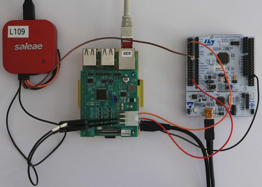
3.1.1. Application test setup
The previously described application is implemented on a STM32 Nucleo board [12]. Nucleos are development
boards, that are provided by ST. These boards are available for almost any 32 −bit processor in their product
range. The used Nucleo board in this prototype is equipped with a L452RE microcontroller. The L452RE is aimed
Author: Dominik Wenger Last change: July 28, 2020 Page 21 of 70Berner Fachhochschule 3 3.1. STM32 SOFTWARE VALIDATION Mikro- und Medizintechnik
at ultra low-power applications and therefore has some special features. It should be pointed out that there is no
need for such a low-power controller in this application. The only reason why the L452RE was selected is because
it was currently available in the lab. Since all ST microcontrollers are providing more or less the same interface to
their peripherals by the hardware abstraction layer (HAL) library, it does not really matter which controller family
is used for such a simple test application.
A proprietary MDB/ICP controller is used to emulate the VMC commands. It was manufactured by the company
Qibixx and is an extension board to the Raspberry Pi. The communication between the Raspberry Pi and it’s
extension board is managed via a 8 bit UART bus with a baud rate of 115 200 bit s−1 .
The Raspberry Pi itself is a model 3+. It’s operating system, called Raspian, is based on debian, thus fairly
familiar out of the box and can easily be accessed over SSH1 .
Additionally, a saleae logic analyzer is used to measure the signals on the bus layer. This device will be able to
measure the signal transition time trough the ST microcontroller.
The following picture shows the final test setup.
Figure 3.2.: Prototype composition with logic analyzer, Raspberry Pi and Nucleo
Emulated VMC (center) to saleae logic analyzer (left)
I Black cable with white label:
MDB/ICP master-to-peripheral line.
I Black cable:
Ground reference.
Emulated VMC (center) to STM32 Nucleo (right)
I Red cable:
MDB/ICP master-to-peripheral data line.
1 The operating system installation and SSH set-up procedure is documented in the git repository of the project.
Author: Dominik Wenger Last change: July 28, 2020 Page 22 of 70Berner Fachhochschule 3 3.1. STM32 SOFTWARE VALIDATION Mikro- und Medizintechnik
I Orange cable:
MDB/ICP peripheral-to-master line. Currently not in use.
I Black cable:
Ground reference.
STM32 Nucleo (right) to saleae logic analyzer (left)
I Brown cable:
Converted message UART output.
3.1.2. Measurements
The logic analyzer finally delivers the measurement results.
Figure 3.3.: Measurement 1: Minimum of a VMC message
The minimum message length (figure 3.3) has a transition time of 1,2001 ms. One has thereby to consider, that
the UART controller has to wait until the inter block timeout has exceeded. This timeout value has been specified
as 1,042 ms. Actually, the value specified in the MDB/ICP standard would be 1 ms. However, in ST’s UART
interface, one can only specify values as multiples of the baud rate period time.
Figure 3.4.: Measurement 2: 35 byte VMC message
It is very pleasant to observe that the transition time does not rise with a higher message length (figure 3.4). The
reason why it is even shorter (1,199 21 ms) than in the previous message could be because the resending of the
converted signal is currently handled in the main routine of the STM32 application and not via interrupts.
Figure 3.5.: Measurement 3: Maximum of a VMC message
When the maximum message length is received (figure 3.5), the transition time is even shorter (0,154 78 ms).
Since the message length is defined with 36 bytes one does not have to wait for the inter block timeout, but can
immediately start with the conversion.
Overall, one can say that the measurement results predict that the STM32 microcontroller will be able to handle
MDB/ICP conversion. An open question is which bus should be used to intercommunicate between the Raspberry
Pi and the extension board. In order to guarantee the total response time of 5 ms, one should theoretically select
an interface which is able to transfer data at a speed of at least 400 000 bit s−1 .
Author: Dominik Wenger Last change: July 28, 2020 Page 23 of 70Berner Fachhochschule 3 3.1. STM32 SOFTWARE VALIDATION Mikro- und Medizintechnik This intercommunication transfer rate is chosen with the following calculation: I Transition time STM32 message reception: 1,2 ms I Intercommunication STM32-Raspberry (35 B at 400 000 bit s−1 ): 0,7 ms I Raspberry Pi transition time (estimated): 2 ms I Intercommunication Raspberry-STM32 (35 B at 400 000 bit s−1 ): 0,7 ms I Transition time STM32 message sending (estimated): 0,2 ms I Total response time (estimated): 4,8 ms Within this intercommunication time, the bus communication overhead is not respected. However, this worst case scenario is fairly unrealistic. In case of a cashless device, one can argue that there is no need for a direct response with process data. The cashless device on the Raspberry Pi could simply decide to respond with a shorter ACK signal to the direct request and will then send the requested data as a response of the next master poll. This fact allows, that the transfer rate could even be slower. Another method to avoid this timing problem could be implemented by using the STM32 as buffer device where standard polls are answered automatically. If the Raspberry Pi sends data to the microcontroller, it will be stored and used for the next poll. This leads to an asynchronous communication which enables a higher flexibility for the MDB/ICP peripheral on the Raspberry Pi. However, the exact behaviour of the Raspberry Pi has to be measured in order to determine which approach is the most appropriate. Since the experiment could confirm that the setup is qualified for the expected tasks, one can now start with the development of the associated hardware. To keep the bus type for intercommunication between both boards flexible, one will implement the signal paths for I2C, UART and SPI on the PCB. Since only one bus type will be needed in the final module, the paths will be equipped with solder bridges which enables to connect and disconnect them. Author: Dominik Wenger Last change: July 28, 2020 Page 24 of 70
Berner Fachhochschule                3                Mikro- und Medizintechnik

                              Part II.

                             Thesis

Author: Dominik Wenger   Last change: July 28, 2020               Page 25 of 70
Berner Fachhochschule 4 Mikro- und Medizintechnik 4. Introduction During the preliminary study, the Multi Drop Bus / Internal Communication Protocol (MDB/ICP), which specifies the internal processes of a vending machine has been studied and was explained to the reader in section 1.2. The Taler payment platform was separated into two independent modules, whereof each one is defined by a specification book in chapter 2. The modules are called: I MDB/ICP converter module I Taler application module For each module, different concepts were elaborated and compared to each other based on their specification book’s requirements. This decision-making process led to the development of two Printed Circuit Boards (PCB). The MDB/ICP converter module’s function is to provide an interface to the vending machine, which translates the MDB/ICP bus messages and sends them in a readable format to the connected peripheral. The hardware interface includes the standard bus connector, signal decoupling optocouplers, and a step down voltage converter for bus power supply. Message conversion is handled by a 32 bit microcontroller, which supports the required 9 bit UART communication. Previous tests have shown, that a microcontroller’s capabilities fulfill the requirements (see chapter 3). During the bachelor’s thesis, a converter module was developed and manufactured. It is further called MDB/ICP gateway and is an extension board to the Raspberry Pi. This gateway provides the above listed hardware interfaces and also has additional features, which will be discussed during the next chapter. Later, an embededded Taler platform was developed. It is based on an interchangeable, open-hardware computing module from the manufacturer Seeed Studios [10]. This module (also called System on Module SoM) consists of a microprocessor, its RAM and an additional eMMC memory block. The platform provides the vending machine interface along with other connectors that will be used to connect a NFC-Reader and a display. Unfortunately, this platform could not be finished during the thesis. The missing part is the design of the PCB. It will take approximately a week of work until the platform is ready for manufacturing. Author: Dominik Wenger Last change: July 28, 2020 Page 26 of 70
Berner Fachhochschule                                    5                        Mikro- und Medizintechnik

5. MDB/ICP Gateway

In this chapter, the development steps of the MDB/ICP gateway will be discussed. The hardware tests will give
an insight about the capabilities of the designed gateway and possible improvements. There was no software
developed for this board. Netherless, some basic ideas about a possible workflow are presented.

The following specification presents a quick overwiew.

Author: Dominik Wenger                    Last change: July 28, 2020                           Page 27 of 70
Berner Fachhochschule 5 5.1. SPECIFICATION SHEET Mikro- und Medizintechnik
5.1. Specification Sheet
MDB/ICP VENDING MACHINE PERIPHERAL GATEWAY FOR RASPBERRY PI
FEATURES
I Standard MDB/ICP interface connector
I Optical decoupled signal lines
I Interface abstraction with microcontroller
I MDB/ICP bus supply
I Up to three independent communication
interfaces to Raspberry Pi
I USB service port
Figure 5.1.: MDB/ICP Gateway
I SD-Card data log interface
I open Hard- and Software APPLICATIONS
I SWD interface I Vending machine peripheral development
I MDB/ICP bus debugging
GENERAL DESCRIPTION
The MDB/ICP gateway is an ideal development tool for A Micro SD-Card connector allows to externally store
everyone who is interested in vending machine periph- process-data. The USB receptacle is meant as a service
eral applications. The gateway follows the MDB/ICP port to live monitor bus-data on an external device.
version 4.2 specifications and allows a reliable interface
abstraction. Open soft- and hardware offer a high de- The gateway is powered by the Raspberry Pi’s 3,3 V
gree of customizability. GPIO header pins. The Power supply from the vending
machine interface serves the Raspberry Pi’s 5V supply
The Raspberry Pi extension board is connected to a pin. The voltage conversion has an efficiency of up to
vending machine trough the provided connector. The 85 % and can optionally be disabled.
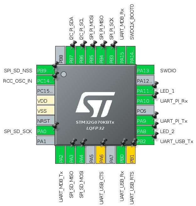
32 bit ST Electronics STM32G070 microcontroller han-
dles the bus data conversion and implements three in- The Serial Wire Debug (SWD) interface allows pro-
dependent communication interfaces (UART, I2C, SPI) gramming and debugging of the microcontroller. Alter-
to the Raspberry Pi. natively, the microcontroller can be programmed trough
the Raspberry Pi I2C or UART.
Figure 5.2.: MDB / ICP Gateway block diagram
Author: Dominik Wenger Last change: July 28, 2020 Page 28 of 70You can also read