Emerging inorganic solar cell efficiency tables (version 2)
←
→
Page content transcription
If your browser does not render page correctly, please read the page content below
TOPICAL REVIEW • OPEN ACCESS

Emerging inorganic solar cell efficiency tables (version 2)
To cite this article: Andriy Zakutayev et al 2021 J. Phys. Energy 3 032003

View the article online for updates and enhancements.

                              This content was downloaded from IP address 192.174.37.51 on 11/05/2021 at 18:19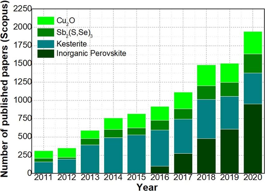
J. Phys. Energy 3 (2021) 032003 https://doi.org/10.1088/2515-7655/abebca
Journal of Physics: Energy
TOPICAL REVIEW
Emerging inorganic solar cell efficiency tables (version 2)
OPEN ACCESS
Andriy Zakutayev1, Jonathan D Major2, Xiaojing Hao3, Aron Walsh4,5, Jiang Tang6, Teodor K Todorov7,
RECEIVED Lydia H Wong8 and Edgardo Saucedo9,∗
22 October 2020
1
REVISED
National Renewable Energy Laboratory (NREL), Golden, CO 80401, United States of America
2
27 January 2021 Stephenson Institute for Renewable Energy, Department of Physics, University of Liverpool (UL), Liverpool L69 7ZF, United Kingdom
3
Australian Centre for Advanced Photovoltaics, School of Photovoltaic and Renewable Energy Engineering, University of New South
ACCEPTED FOR PUBLICATION
3 March 2021 Wales (UNSW), Sydney, NSW 2052, Australia
4
Department of Materials, Imperial College London (ICL), Exhibition Road, London SW7 2AZ, United Kingdom
PUBLISHED 5
16 April 2021
Yonsei University (YU), Seoul 03722, Republic of Korea
6
Wuhan National Laboratory for Optoelectronics, Huazhong University of Science and Technology (HUST), 430074 Wuhan, People’s
Republic of China
Original content from 7
IBM Thomas J. Watson Research Center, Yorktown Heights, New York 10598, United States of America
this work may be used 8
under the terms of the
School of Materials Science & Engineering, Nanyang Technological University (NTU), Singapore 639789, Singapore
9
Creative Commons Universitat Politècnica de Catalunya (UPC), Campus Diagonal-Besòs, 08930 Sant Adrià del Besòs- Barcelona, Spain
∗
Attribution 4.0 licence. Author to whom any correspondence should be addressed.
Any further distribution E-mail: edgardo.saucedo@upc.edu
of this work must
maintain attribution to
Keywords: thin film inorganic photovoltaics, emerging photovoltaic technologies, conversion efficiency, solar energy
the author(s) and the title
of the work, journal
citation and DOI.
Abstract
This paper presents the second version of the efficiency tables of materials considered as emerging
inorganic absorbers for photovoltaic solar cell technologies. The materials collected in these tables
are selected based on their progress in recent years, and their demonstrated potential as future
photovoltaic absorbers. The first part of the paper consists of the guidelines for the inclusion of the
different technologies in this paper, the verification means used by the authors, and
recommendation for measurement best practices. The second part details the highest world-class
certified solar cell efficiencies, and the highest non-certified cases (some independently confirmed).
The third part highlights the new entries including the record efficiencies, as well as new materials
included in this version of the tables. The final part is dedicated to review a specific aspect of
materials research that the authors consider of high relevance for the scientific community. In this
version of the efficiency tables, we are including an overview of the latest progress in quasi
one-dimensional absorbers, such as antimony chalcogenides, for photovoltaic applications.
Abbreviations
Eff. (%) conversion efficiency obtained under AM1.5 illumination in percentage
V OC (V) open circuit voltage in volts
J SC short circuit current in milli-Amperes by square centimetre
(mA cm−2 )
FF (%) fill factor in percentage
Eg (eV) bandgap in electronvolt
AZO ZnO:Al
ITO In2 O3 :SnO2
Spiro- 2,2′ ,7,7′ -tetrakis[N,N-di(4-methoxyphenyl)amino]-9,9′ -spirobifluorene (C81 H68 N4 O8 )
OMeTAD
TBAI tetrabutylammonium iodide
EDT 1,2-ethanedithiol
PTB7 poly[[4,8-bis[(2-ethylhexyl)oxy]benzo[1,2-b:4,5-b’]dithiophene-2,6-diyl][3-fluoro-2-[(2-
ethylhexyl)carbonyl]thieno[3,4-b]thiophenediyl]] ((C41 H53 FO4 S4 )n )
ARC anti-reflection coating
CuPc+ copper phthalocyanine
© 2021 The Author(s). Published by IOP Publishing LtdJ. Phys. Energy 3 (2021) 032003 A Zakutayev et al
PTAA poly[bis(4-phenyl)(2,4,6-trimethylphenyl)amine ((C21 H19 N)n )
PCBM [6,6]-phenyl C61 butyric acid methyl ester (C72 H14 O2 )
mp-TiO2 mesoporous TiO2
TiO2 -BL TiO2 blocking layer
PCPDTBT poly[N-9′ -heptadecanyl-2,7-carbazole-alt-5,5-(4,7-di-2-thienyl-2′ ,1′ ,3′ -benzothiadiazole]
((C43 H47 N3 S3 )n C12 H10 )
PEDOT:PSS poly(2,3-dihydrothieno-1,4-dioxin)-poly(styrenesulfonate)
P3HT poly(3-hexylthiophene-2,5-diyl) ((C10 H14 S)n )
PEG poly(ethylene glycol)
F8 poly(9,9-di-noctylfluorenyl-2,7-diyl)
Q-1D quasi one-dimensional
1. Introduction
1.1. Scope of the paper
Several photovoltaic technologies have now reached the point where they are mature enough, to reach the
market and the progress in their power conversion efficiencies are summarized regularly in ‘Solar Cell
Efficiency Tables’ [1]. Crystalline and multi-crystalline Si modules are the industrial standard but a-Si,
Cu(In, Ga)(S, Se)2 , CdTe, organic photovoltaic, dye-sensitized solar cells, etc have all been commercialized to
varying degrees of success. Whilst these technologies could feasibly cover the majority of photovoltaic
applications, increasing the diversity of viable photovoltaic materials will allow for greater adaptability as the
technology continues to expand and develop. Additionally, most of the established platforms face challenges
related to either the use of critical raw materials, toxic elements, long-term stability, conversion efficiency
limitations, cost or low technological flexibility (e.g. incompatibility with flexible substrates, or transparent
concepts). These are all important considerations that must be taken into account as the field begins to look
towards an era of terawatt level photovoltaic power generation.
The limitations of the mature technologies encourage a continued search for new materials, as none of
the established technologies represent the ‘perfect’ photovoltaic material. The purpose of continued
exploratory research is to identify absorbers that can bring additional benefits and/or may allow the
development of novel applications. New inorganic materials including chalcogenides (sulphides, selenides,
tellurides), oxides, pnictides (nitrides, phosphides), halides (mainly bromides and iodides) and mixed-anion
compounds (e.g. sulfo-iodites) have proved a fruitful area of research and attracted a lot of attention. There
are numerous examples published in recent years showcasing the capability of these materials to act as
photovoltaic absorbers. Respectable device efficiencies have been reported for numerous cell platforms
despite their typically being only limited attempts at fabrication and often with only specific groups
contributing to their progresses. Several of these emerging cell structures have shown enough development
to identify them as potential future technological solutions. As a result, there has been a resurgent interest
from the scientific community in emerging photovoltaic solar cell absorbers, as is shown in figure 1, where
the number of papers published on this topic has increased significantly in the past decade. Notably, starting
from around 300 papers published in this topic in 2011, almost 2000 were published in 2020 in total in the 4
main emerging inorganic photovoltaic technologies, implying an impressive annual growth rate close to 25%
in the last 10 years. Even faster increase in number of publications has been happening in organic and hybrid
materials, as discussed in the recent publication on ‘Device Performance of Emerging Photovoltaic Materials
(Version 1) [2].
Given the continually developing nature of the research field and the large number of emerging inorganic
photovoltaic materials, this paper was conceived to collate information on the current status of the most
promising materials in form of efficiency tables, collecting and summarizing the most relevant information
available in the literature. This includes certified efficiencies in one of the six special centres available in the
world, as well as independently measured examples with a description of the means of efficiency verification
(or lack thereof). The main aim of these tables is to provide researchers working on emerging inorganic
technologies with a valuable information resource by condensing all the spread information about these
fascinating materials, but also to establish a forum for the discussion moving forward. It is hoped that these
tables will evolve with the field and with input from the researchers in the community, informing future
versions to include new champion devices or emerging technologies of note. This second edition of the tables
[3] aims to support and inspire future research in the emerging inorganic solar cells.
1.2. Structure of the paper
The paper is structured in four sections, with the following details:
Section 1 is the present section, giving an overview of the paper, a description of its structure, an
explanation about the criterion used to select the materials included in the different efficiency tables, and a
2J. Phys. Energy 3 (2021) 032003 A Zakutayev et al
Figure 1. Number of published papers in the last 10 years referring to emerging photovoltaics, including kesterite, inorganic
perovskite (CsPbI3 , CsPbB3 and related materials), Sb2 (S,Se)3 and Cu2 O (extracted from Scopus in January 2021).
description of the recommended procedures for the correct J–V in-house illuminated curve measurement,
extraction of corresponding optoelectronic parameters, as well other additional devices information that the
authors consider of high relevance for emerging photovoltaic technologies.
Section 2 contains the efficiency tables split into two categories. The first table summarizes all the
world-class certifications available in the literature, and compiled by the authors. For this table we consider
certified devices with efficiency higher than 5% and area larger than 0.1 cm2 . Exceptions of these
considerations are summarized at the end of the table. The second table collects all the devices that are
non-certified but can be confirmed using specific procedure, with efficiency higher than 1% and area larger
than 0.1 cm2 . Exceptions of these considerations are also summarized at the end of the table. In each of these
two tables, the materials are organized firstly depending on the type of compounds (oxides, chalcogenides,
pnictides, halides, etc), and then in terms of complexity from less to more atoms in the structure.
Section 3 provides a brief description of new entries in terms of new efficiency records but also new
materials included in the tables, with a brief review of the last and most impacting progresses reported in
these technologies.
Section 4 aims to bring to the scientific community a perspective review of a specific topic that the
authors have identified as very timely and with high relevance. In this second edition of the efficiency tables,
the authors have invited Professor Jiang Tang from Huazhong University of Science and Technology (HUST),
China, to review the last progresses in Q-1D materials for photovoltaic applications, including the impressive
achievements in Sb2 (S,Se)3 compounds.
1.3. Criterion for technology selection
For selecting the materials included in the efficiency tables, the authors have defined the following criterion:
Table 1 (World class certification): fully inorganic technologies with certified materials in one of the six
world class certifying centres, with efficiency higher than 5% and area larger than 0.1 cm2 . Exceptions to
these rules are collected separately at the end of the table.
Table 2 (Non world class certification or in house measurements): fully inorganic technologies of
non-certified materials with efficiency higher than 1%, verification through external quantum efficiency
(EQE) measurement, or independent confirmation by a second organization, and area larger than 0.1 cm2 .
Exceptions to these rules are collected separately at the end of the table.
1.4. General guidelines for efficiency measurement
There are several important documents and organization that define solar cell efficiency measurements,
including IEC 60904-3:2008 by International Electrotechnical Commission for general standards and ASTM
G-173-03 by ASTM International for Test Methods and Reference Cells. Certification measurements
following these standards are usually performed by one of the internationally recognized institutions, such as
NREL (USA), AIST (Japan), CSIRO (Australia), Fraunhofer ISE (Germany), CNIM and NPVM (China) or a
few commercial organizations (e.g. Newport), and the records certified by five of them (i.e. NREL, AIST,
CSIRO, Fraunhofer ISE, and Newport) are published bi-annually in ‘solar cell efficiency tables’ [1] for
3Table 1. List of certified single-junction record cells under global AM1.5 spectrum (1000 W m−2 ) at 25 ◦ C, including relevant optoelectronic parameters and important additional data (IEC 60 904-3: 2008, ASTM G-173-03 global).
Material Eff. (%) VOC (V) J SC (mA cm−2 ) FF (%) Area (cm2 ) Eg (eV) Device structure Certifying centre/date Comments
Sb2 Se3 (substrate) 9.2 0.400 32.6 70.3 0.26 1.18 Glass/Mo/MoSe2 /Sb2 Se3 / CNIM (2018) Hebei Key Laboratory of Optic-Electronic
ZnO/AZO Information Materials, Hebiei University,
China [4]. Substrate geometry structure
incorporating core–shell nanowire
approach. Absorber deposited by CSS.
0.731 21.74 69.3 0.2339 1.5 Glass/Mo/CZTS/CdS/ NREL (2017)
J. Phys. Energy 3 (2021) 032003
Cu2 ZnSnS4 (CZTS) 11.0 ± 0.2 UNSW [5]. Absorber prepared by
i-ZnO/ITO/Al/MgF2 sputtering Cu/ZnS/SnS, and reactive
annealing
Cu2 ZnSn(S0.25 Se0.75 )4 (CZTSSe) 12.6 ± 0.3 0.513 35.2 69.8 0.4209 1.13 Glass/Mo/CZTSSe/CdS/ Newport (2013) IBM [6]. Absorber prepared by spin-coating
ZnO/ITO/Ni/Al/MgF2 a hydrazine-based solution, solution and
reactive annealing.
Cu2 ZnSn(Sy Se1−y )4 (CZTSSe) 12.62 ± 0.29 0.541 35.35 65.9 0.4804 NA Glass/Mo/CZTSSe/CdS/ Newport (2018) DGIST [7]. Absorber prepared by
ZnO/ITO/Ni/Al/MgF2 sputtering Sn/Cu/Zn and reactive
4
annealing.
Cu2 ZnSnSe4 (CZTSe) 12.50 0.491 37.37 68.2 0.24 1.04 Glass/Mo/CZTSe/CdS/ NPVM (2019) UNSW/Jinan University [8]. Absorber
ZnO/AZO/Ni/Al/MgF2 prepared by sputtering Cu/Zn/Sn and
reactive annealing in mixed Se/Ar vapor.
Notable exceptions
a
Cu2 O 3.97 1.204 7.37 44.70 0.15 2.2 MgF2 /Al/Al:ZnO/Ga2 O3 / NREL (2014) MIT, Harvard University Cambridge and
Cu2 O/Au NREL [9]. Electrochemical deposition.
CsPbI3 13.58 1.1626 15.246 76.63 0.058 NA Al/MoOx /Spiro-OMeTAD/ NREL (2017) NREL, University of Washington and
CsPbI3 /TiO2 /SnO2 :F/ University of Colorado [10]. Coupled
Glass/MgF2 quantum dots films.
SnS 4.36a 0.372 20.2 58.0 0.24 1.1 Glass/Mo/SnS/SnO2 / NREL (2014) Department of Chemistry and Biology,
Zn(O,S):N/ZnO/ITO Harvard University, Cambridge, USA [11].
ALD deposition of absorber followed by
annealing in H2 S.
Q-1D Sb2 Se3 (superstrate) 7.6 0.420 29.9 60.4 0.091b 1.18 Glass/ITO/CdS/Sb2 Se3 /Au CNIM (2017) Sargent Joint Research Center, Wuhan
National Laboratory for Optoelectronics
and School of Optical and Electronic
Information, Huazhong University of Science
and Technology, Wuhan, China [12]. Vapour
transport deposition.
(Continued)
A Zakutayev et alJ. Phys. Energy 3 (2021) 032003
Table 1. (Continued.)
−2 2
Material Eff. (%) VOC (V) J SC (mA cm ) FF (%) Area (cm ) Eg (eV) Device structure Certifying centre/date Comments
Q-1D Sb2 (S,Se)3 10.0 0.655 24.07 63.5 0.0889 1.49 Glass/FTO/CdS/Sb2 Se3 /Spiro-OMeTAD/Au CNIM (2019) University of Science and Technology
of China, China [13]. Hydrothermal
deposition and annealing.
PbS 9.88 0.635 21.6 71.9 0.05b NA Glass/ITO/ZnO/PbS(TBAI)/PbS(EDT)/Au Newport (2015) Wuhan National Laboratory for
5
Optoelectronics and School of Optical
and Electronic Information, Huazhong
University of Science and Technology,
Wuhan, China [14]. Spin coating of PbS
colloidal quantum dots.
AgBiS2 6.31 0.450 22.1 63.0 0.017b 1.3 Glass/ITO/ZnO/AgBiS2 /PTB7/MoO3 Newport (2016) ICFO—Institut de Ciències Fotòniques,
The Barcelona Institute of Science and
Technology, Barcelona, Spain [15].
Layer-by-layer spin coat deposition from
nanocrystal solution.
a
Certified efficiency below 5%.
b
Area of the certified cell below 0.1 cm2 (total area).
NA—not available.
A Zakutayev et alTable 2. List of non-certified single-junction record cells under global AM1.5 spectrum (1000 W m−2 ) at 25 ◦ C, including relevant optoelectronic parameters, the means of verification and important additional data (IEC 60 904-3:
2008, ASTM G-173-03 global).
Material Eff. (%) V OC (V) J SC (mA cm−2 ) FF (%) Area (cm2 ) Eg (eV) Device structure Means of verification Institutions and Comments
Pnictides
Zn3 P2 6.0 0.492 14.9 71.0 0.70 NA ZnS/Mg/Ag:Zn3 P2 /Ag No EQE results U. Delaware [16]. CVT grown thick
wafer absorber measured in AMI
illumination. Measured under a
J. Phys. Energy 3 (2021) 032003
simulated intensity of 87.5 mW cm−2 .
ZnSnP2 3.44 0.47 12.3 59 0.785 1.68 Al/ZnO:Al/ZnO/(Cd, EQE, In-house Ritsumeikan University [17]. Bulk
Zn)S/ZnSnP2 /Cu ZnSnP2 crystals with 200 um thickness
grown by flux method.
Oxides
BiMnO3 :BiMn2 O5 4.2 1.5 4.9 58 0.5 1.25 Nb:SrTiO3 /BiMnO3 :BiMn2 O5 / EQE, In-house INRS Canada [18]. Absorbers grown by
6
In2 O3 :SnO2 PLD on single crystal substrate.
Chalcogenides
CuSbSe2 4.7 0.336 26.3 53.0 0.2 NA Glass/Mo/CuSbSe2 /ZnO/AZO EQE, In-house National Renewable Energy Laboratory,
Golden, USA [19]. Sputtering from
binary Cu2 Se and Sb2 Se3 targets.
CuSbS2 3.2 0.470 15.6 43.6 0.45 1.4–1.9 Glass/Mo/CuSbS2 /CdS/ EQE, In-house New and Renewable Energy Research
ZnO/AZO Division, Korea Institute of Energy
Research, Daejeon, South Korea [20].
Sulfurization of nanoparticle inks.
Cu2 CdSnS4 7.96 0.624 22.3 57.2 0.16 1.42 Glass/Mo/CCdTS/CdS/ EQE, In-house NTU, Singapore [21]. Absorber
ITO/Ag prepared by spin-coating using
2-methoxyethanol-based solution.
Cu2 BaSnS4 (substrate) 1.7 0.698 5.3 46.9 0.2 2.01 Glass/Mo/CBaTS/CdS/ZnO/ EQE, In-house Central South University, UNSW, Shen
ITO/Al Zhen University, Xiamen University [22].
Absorber prepared by spin-coating using
a 2-methoxyethanol-based solution.
Cu2 BaSnS4 (superstrate) 2.0 0.933 5.1 42.9 0.2 2.04 CdS:O/CdS/ZnO/AZO EQE, In-house The University of Toledo [23]. Absorber
prepared by sputtering method.
Cu2 FeSnS4 3.0 0.610 9.3 52.0 0.1 1.5 ITO/Cu-NiO/CFeTS/ EQE, In-house Indian Association for the Cultivation
Bi2 S3 /ZnO/Al of Science [24]. Absorber prepared by
SILAR method.
(Continued)
A Zakutayev et alTable 2. (Continued.)
−2 2
Material Eff. (%) V OC (V) J SC (mA cm ) FF (%) Area (cm ) Eg (eV) Device structure Means of verification Institutions and Comments
Cu2 CdSn(S0.xx Se0.yy )4 2.8 0.356 18.8 41.6 0.405 1.55 Glass/Mo/CCdTSSe/CdS/ EQE, In-house Changchun Institute of Applied Chemistry,
ZnO/ITO/Al Chinese Academy of Sciences [25].
Absorber prepared by spin-coating an
ethanol, butyldithiocarbamic acid, and
thioglycolic acid -based solution.
Cu2 BaSn(S0.xx Se0.yy )4 5.2 0.611 17.4 48.9 0.425 1.55 Glass/Mo/CBaTSSe/CdS/ EQE, In-house Duke University, IBM [26]. Absorber
ZnO/ITO/Ni/Al prepared by co-sputtering using Cu, Sn,
and BaS
Cu2 ZnGe(S0.xx Se0.yy )4 6.0 0.617 NA NA 0.25 1.47 Glass/Mo/CZGeSSe/CdS/ EQE, In-house ZSW, CNRS [27]. Absorber prepared
J. Phys. Energy 3 (2021) 032003
ZnO/AZO/Ni/Al by doctor-blade coating a DMF-based
solution.
Cu2 ZnGeSe4 8.5 0.625 24.4 55.7 0.52 1.39 Glass/Mo/CZGSe/CdS/ EQE, in-house Institut des Materiaux Jean Rouxel
IZO/AZO/Ni/Al (IMN) [28]. HCl and (NH4 )2 S solution
for surface treatment, air annealing at
200 ◦ C for 60 min.
Ag2 ZnSnSe4 5.18 0.504 21.0 48.7 0.45 1.35 FTO/AgZTSe/MoO3 /ITO/ EQE, In-house IBM, UCSD [29]. Absorber prepared by
7
Ni/Al coevaporation of Ag, Zn, Sn, and cracked
Se.
Cu2 ZnCdSnS4 12.60 0.640 27.8 71.0 0.16 1.34 Glass/Mo/CZCTS/CdS/ EQE, in-house, active area Shenzhen University [30]. Device
ITO/Ag annealed at 300 ◦ C in air for 8 min.
(Ag0.05–0.3 Cu0.95–0.7 )2 ZnSn(S,Se)4 11.2 0.464 36.2 66.5 0.21 Graded Glass/Mo/ACZTSSe/CdS/ EQE, in-house Henan University, China [31]. Spin
ZnO/ITO/Ag coating of ethanol based solutions.
(Ag0.05 Cu0.95 )2 (Zn0.75 Cd0.25 )S4 10.1 0.650 23.4 66.2 0.16 1.4 Glass/Mo/ACCdZTS/CdS/ EQE, in-house NTU, Singapore; HZB, Germany [32].
ITO/Ag Spin coating of 2-methoxyethanol based
solution.
Cu2 Zn(Sn0.78 Ge0.22 )Se4 12.3 0.527 32.2 72.7 0.519 1.11 Glass/Mo/CZTGTSe/CdS/ EQE, in-house AIST, Japan [33]. Co-evaporation and
ZnO/AZO/Ag/ARC reactive annealing.
(Li0.06 Cu0.94 )2 ZnSn(S,Se)4 11.6 0.531 33.7 64.8 0.285 1.13 Glass/SiOx /Mo/LiCZTSSe/ EQE, in-house EMPA, Switzerland; Universidad
CdS/ZnO/AZO/Ni/Al/MgF2 Autónoma de Madrid, Spain; HZB,
Germany [34]. Spin coating of DMSO
based solution.
Cu2 (Zn0.95 Mn0.05 )Sn(S,Se)4 8.9 0.418 33.7 63.3 0.34 1.06 Glass/Mo/CMZTSSe/CdS/ EQE Nankai University, China; National
ZnO/AZO/Ni/Al Institute of Material Science, Japan [35].
Spin coating of 2-methoxyethanol based
solution.
Cu2 Zn0.96 Mg0.04 Sn(S,Se)4 7.2 0.419 37.2 46.5 0.3 1.01 Glass/SiOx /Mo/CZMTSSe/ Universidad Autónoma de Madrid, Spain
CdS/i-ZnO/AZO/Ni/ [36]. Precursor solution prepared by
Al/MgF2 dimethyl sulfoxide (DMSO).
(Continued)
A Zakutayev et alTable 2. (Continued.)
Material Eff. (%) V OC (V) J SC (mA cm−2 ) FF (%) Area (cm2 ) Eg (eV) Device structure Means of verification Institutions and Comments
Cu2 SnS3 5.1 0.290 34.5 51.3 0.3 0.95 Glass/Mo/CTS/CdS/ EQE, in-house Ritsumeikan University, Japan [37].
i-ZnO/AZO/Ni/Al Absorber prepared by Sputtering of
Cu-SnS2 compound, and e-beam
evaporation of NaF.
Cu2 ZnSn0.91 I0.09 (S,Se)4 7.19 0.393 32.12 56.96 0.21 1.075 Mo-foil/CZTISSe/CdS/ EQE, in house Fujian JIangxia University, Fuzhou, China
i-ZnO/ITO/Ag [38]. Absorber is deposited on flexible Mo
foil by spin coating of precursor solution
based on 1,2-ethanedithiol (edtH2) and
1,2-ethylenediamine (en) solution.
10.8 0.455 36.48 65.05 0.21 1.162 Glass/Mo/CZTGSSe/CdS/ EQE, in house Henan University [31]. With ARC; thin film
J. Phys. Energy 3 (2021) 032003
Cu2 ZnSnx Ga1−x (S,Se)4
iZnO/ITO/Ag/MgF2 is deposited by spin coating of precursor
solution based on ethylendiamine and 1,2
ethanedithiol.
Cu2 Sn1−x Gex S3 6.73 0.442 26.6 57.1 0.17 1.09 Glass/Mo/CTGS/CdS/ EQE, in-house Toyota Central Research & Development
ZnO:Ga/Al Laboratories, Japan [39]. Co-sputtering
Cu-Sn-Ge with two layer stack.
8
Notable exceptions
Oxides
a
Cu2 O 8.1 1.2 10.4 65.0 0.03 2.2 MgF2 /Al:ZnO/Zn0.38 Ge0.62 O/ No EQE results Kanazawa I. T [40]. Cu2 O sheets oxidized
Cu2 O:Na/Au from Cu foils
Bi2 FeCrO6 8.1 0.84 20.6 46.0 NAa 1.4 Sn:In2 O3 /Bi2 FeCrO6 /SrRuO3 EQE, In-house INRS Canada [41]. PLD absorber with
3-layer stack.
Pnictides
a
InP 7.3 0.57 17.4 73.0 0.0625 1.32 Al/ZnO:Al/i-ZnO/ EQE, In-house Purdue U., The U. of California, and The
InP:Zn/Au-Zn-Au Pennsylvania State U [42]. Pulsed laser
deposition.
(In,Ga)N 3.0 1.8 2.6 64.0 0.046a NA SiO2 /Au/(Mg:GaN/GaN)/ No EQE results Texas Tech [43]. MOCVD MQW absorber
(In,Ga)N/Si:GaN
ZnSnN2 1.5 0.36 7.5 57.0 0.06a 1.4 Au/ZnSnN2 /Al2 O3 /SnO No EQE results Ningbo, China [44]. Sputtered absorber.
Halides
a
BiI3 1.2 0.607 5.3 37.6 0.04 1.72 Au/F8/BiI3 /TiO2 /SnO2 :Fb EQE, In-house U. Bristol [45]. Spin coating of Bi(NO3 )3
and thiourea, followed by thermolysis at
200 ◦ C to produce a homogeneous Bi2 S3
film that is subsequently iodinated upon
exposure to the I2 gas.
A Zakutayev et al
(Continued)Table 2. (Continued.)
−2 2
Material Eff. (%) V OC (V) J SC (mA cm ) FF (%) Area (cm ) Eg (eV) Device structure Means of verification Institutions and Comments
CsPbBr3 10.91 1.498 9.78 74.47 0.09a 2.35 Ag/Spiro-OMeTAD/ EQE, In-house, reverse voltage Okinawa Institute of Science and
CsPbBr3 /c-TiO2/ Technology Graduate University (OIST),
SnO2 :Fb Japan and Hefei University of Technology,
China [46]. Thermal evaporation.
CsPbI3 19.03 1.137 20.23 82.7 0.1 N.R. Ag/Spiro-OMeTAD/ EQE, In-house Shanghai Jiao Tong
J. Phys. Energy 3 (2021) 032003
CsPbI3 /c-TiO2 /SnO2 :Fb University, China [47]. Spin
coating and soft annealing.
CsPbI2 Br 16.79 1.32 15.32 83.29 0.09a 1.91 Au/Spiro-OMeTAD/ EQE, In-house Shaanxi Normal University, China [48].
CsPbI2 Br/TiO2 /SnO2 :Fb Spin coating and soft annealing.
CsPbIBr2 11.1 1.21 12.25 74.82 0.078 2.07 Ag/Spiro-OMeTAD/ EQE, in-house Soochow University, China [49]. Spin
PEG:CsPbIBr2 /TiO2 /SnO2 :Fb coating and soft annealing.
CsPb0.75 Sn0.25 IBr2 11.53 1.21 12.57 75.8 0.1 1.78 Au/Spiro-OMeTAD/ EQE, In-house Tsinghua University-China, The
CsPb0.75 Sn0.25 IBr2 /C60/ University of Washington-USA, The
9
TiO2 /In2 O3 :SnO2 Hong Kong University of Science and
Technology-Hong Kong, City Univer-
sity of Hong Kong-Hong Kong [50]. Spin
coating and soft annealing.
CsPb0.95 Eu0.05 I2 Br 13.7 1.22 14.6 76.6 0.16 1.91 Au/Spiro-OMeTAD/ EQE, In-house Wuhan U. Technology, EPFL, Nankai U
CsPb0.95 Eu0.05 I2 Br/TiO2 / [51]. Precursor solution by spin coating.
SnO2 :Fb Some hysteresis is observed.
CsSnBr3 2.2 0.42 9.1 57.0 NA 1.75 Au/Spiro-OMeTAD/ EQE, In-house Weizmann Institute of Science [52]. Spin
CsSnBr3 /TiO2 /SnO2 :Fb coating. The EQE integration gives
2 mA cm−2 less current density.
CsSnI3 4.8 0.382 25.7 49.1 ∼0.15 1.30 Au/PTAA/CsSnI3 /TiO2 / EQE, In-house Northwestern University and Mitsubishi
SnO2 :Fb Chemical Group Science & Technology
Research Center [53]. Spin coating with
hydrazine. Integrated EQE gives J sc of
approximately 24 mA cm−2 .
CsSn0.5 Ge0.5 I3 7.1 0.63 18.6 60.6 0.1 1.50 Au/Spiro-OMeTAD/ EQE, In-house Brown U., U. of Nebraska-Lincoln,
CsSn0.5 Ge0.5 I3 /PCBM/ Worcester Polytechnic Institute, and
SnO2 :Fb Okinawa Institute of Science and
Technology Graduate University [54].
Powder synthesized by solid-state
reaction and thermally evaporated.
(Continued)
A Zakutayev et alTable 2. (Continued.)
Material Eff. (%) V OC (V) J SC (mA cm−2 ) FF (%) Area (cm2 ) Eg (eV) Device structure Means of verification Institutions and Comments
Mixed-anions
Q-1D Sb2 S3 -SbSI 6.08 0.62 14.92 0.66 0.16 1.76/2.1 Au/PCPDTBT/Sb2 S3 -SbSI/ EQE, in-house Ulsan National Institute of Science and
mp-TiO2 /TiO2 -BL/ Technology, Republic of Korea [55]. Sb2 S3
SnO2 :Fb by chemical bath deposition and SbSI by
J. Phys. Energy 3 (2021) 032003
hot plate of powders.
Q-1D SbSI 3.05 0.58 9.11 57.7 0.16 2.15 Au/PCPDTBT/SbSI/ Ulsan National Institute of Science and
mp-TiO2 /TiO2 -BL/ Technology, Convergence Research
SnO2 :Fb Center for Solar Energy DGIST and
Korea Research Institute of Chemical
Technology (KRICT), Republic of Korea [56].
Sb2 S3 by chemical bath deposition, SbI3
by spin coating and further soft hot plate.
10
10–20 cycles.
Q-1D Sb0.67 Bi0.33 SI 4.07 0.53 14.54 57.7 0.16 1.62 Au/PCPDTBT/ EQE, in-house Ulsan National Institute of Science and Tech-
Sb0.67 Bi0.33 SI/ nology and Korea Research Institute of Chem-
mp-TiO2 /TiO2 - ical Technology (KRICT), Republic of Korea
BL/SnO2 :Fb [57]. Sb2 S3 by chemical bath deposition,
BiI3 by spin coating and further soft hot
plate, with repeated cycles.
Q-1D BiSI 1.32 0.445 8.44 35.14 0.04a 1.57 Au/F8/BiSI/SnO2 /SnO2 :Fb EQE, in-house U. Bristol [58]. Spin coating and soft
annealing.
Chalcogenides
a
Se 6.5 0.969 10.6 63.4 0.027 1.95 Glass/FTO/TiO2 /ZnMgO/ EQE, In-house IBM Thomas J. Watson Research Centre,
Se/MoO3 /Au Yorktown Heights, USA [59]. Thermal
evaporation of Se at room temperature
followed by post-deposition annealing.
GeSe 1.5 0.240 14.5 42.6 0.09a 1.1–1.2 Glass/ITO/CdS/GeSe/Au EQE, In-house Beijing National Laboratory for Molecular
Sciences, Key Laboratory of Molecular
Nanostructure and Nanotechnology, Institute
of Chemistry, Beijing, China [60]. Rapid
thermal sublimation.
(Continued)
A Zakutayev et alTable 2. (Continued.)
Material Eff. (%) V OC (V) J SC (mA cm−2 ) FF (%) Area (cm2 ) Eg (eV) Device structure Means of verification Institutions and Comments
J. Phys. Energy 3 (2021) 032003
Q-1D Sb2 S3 7.5 0.711 16.1 65.0 0.16 1.7 Glass/FTO/TiO2 /mp-TiO2/ EQE, In-house Division of Advanced Materials, Korea
Sb2 S3 /PCPDTBT/ Institute of Chemical Technology, Daejeon,
PEDOT:PSS/Aub Republic of Korea [61]. Chemical bath
deposition followed by additional
sulfurization.
Q-1D Sb2 (Sx Se1−x )3 10.5 0.664 23.8 66.3 0.09 1.55 Glass/FTO/Sb2 (Sx Se1−x )3 /Au EQE, in house Hefei National Laboratory for Physical Sci-
11
ences at Microscale, CAS Key Laboratory of
Materials for Energy Conversion, Department
of Materials Science and Engineering, School
of Chemistry and Materials Science, Univer-
sity of Science and Technology of China, Hefei
[62].
Bi2 S3 3.3 0.700 10.7 45.0 0.18 1.2 Glass/ITO/P3HT:Bi2 S3 /MoOx / EQE, In-house Department of Chemical and Biological
Aub Engineering, Princeton University, USA [63].
Percolated Bi2 S3 network with P3HT.
Cu2 CdGeSe4 4.2 0.464 23.3 39.0 0.02a 1.27 Graphite/Epoxy/CCdGeSe/ EQE, In-house Tallinn University of Technology [64].
CdS/ZnO/AZO/glue/Ag/glass Absorber prepared by molten salt method
using CdI2 and KI as fluxes. Monograin-
based device.
a
Area of the non certified cell below 0.1 cm2 or not reported.
b
Devices includes at least one organic carriers transport layer.
NA—not available; PC—phtalocyanine.
A Zakutayev et alJ. Phys. Energy 3 (2021) 032003 A Zakutayev et al
well-established solar cell technologies. However, for the emerging solar cell technologies that are developing
very quickly, such certification is not always practical, so only in-house measured photovoltaic (PV)
efficiencies are often reported. Thus, it is important to review here common best practices for in-house solar
cell efficiency measurements. The most basic requirements for lab-based solar cell efficiency measurements
include:
(a) using the air mass 1.5 spectrum (AM1.5) for terrestrial cells by choosing the highest-quality solar simu-
lator available;
(b) applying one-sun of illumination with intensity of 1000 W cm−2 by adjusting the cell/simulator distance
to match the expected current of the reference cell;
(c) controlling cell temperature during the measurement to 25 ◦ C using active cooling or heating;
(d) using four-point probe geometry to remove the effect of probe/cell contact resistance.
In addition, there are several other best practices to follow.
(a) Areas of the measured solar cells have to be carefully defined using device isolation and/or light masking;
this is particularly relevant to absorbers with large carrier diffusion lengths.
(b) Current density–voltage measurements have to be performed in both forward and reverse directions,
which is especially important for emerging absorbers with tendency for hysteresis.
(c) EQE measurement has to be reported to assist with spectral correction, and integrated with the AM1.5
reference spectrum to obtain the current, to be compared to reported J sc .
(d) Statistical analysis results, including the number of the solar cells measured, and the mean values have to
be mentioned.
(e) Short-time evolution of the reported deficiency has to be verified at the maximum power point or with
the photocurrent at maximum power point.
(f) Long-time stability analysis is encouraged, under light and electrical bias, with measured temperature
and humidity.
(g) For multi-junction solar cells, the illumination bias and voltage bias used for each cell have to be reported.
Finally, we reemphasize that these are just guidelines for in-house solar cell measurements, when external
certification is not practical. However, researchers working on emerging solar cell technologies are strongly
encouraged to strive towards perfection and consider submission of their devices to one of the
internationally recognized institutions.
2. Efficiency tables
Table 1 presents the list of materials that have been identified for the authors as certified solar cells, and are
considered as the highest reported conversion efficiency in their class of technology. The last part of table 1
collects the technologies that being certified, do not fulfil some of the criteria used for including them in the
principal section. Table 2 contains the list of materials and device performance for non-certified solar cells.
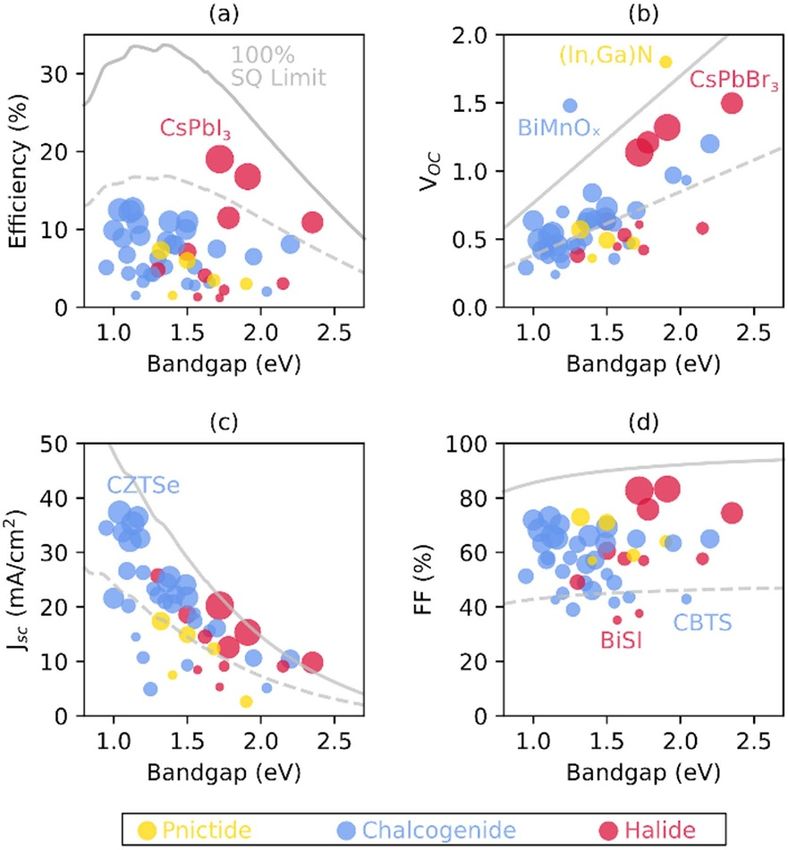
The combined data from both tables is plotted in figure 2, where it is separated into three categories: metal
pnictides (e.g. ZnSnP2 ), chalcogenides (e.g. PbS), and halides (e.g. BiI3 ).
3. New entries
3.1. Oxides
There have been no new records reported for solar cells with oxide absorbers, but several important advances
have been made. For Cu2 O absorbers with Ga2 O3 buffer layers grown by chemical vapour deposition, the
V oc of 1.78 V has been achieved albeit with small photocurrent of 2 mA cm−2 [65]. This demonstrates the
ability of Cu2 O to reach >80% of V oc entitlement based on Shockley–Queisser limit (Eg = 2.2 eV), and
achieve in the future >13% efficiency for thicker absorber layers based on numerical models [66]. A low
damage magnetron sputtering method for fabrication of ZnO contacts to Cu2 O solar cells has been also
recently demonstrated [67]. The progress in Cu2 O and other oxide solar cells has been summarized in a
recent roadmap article [67] and a book chapter [68].
As of the more exotic oxide absorbers with perovskite structure and ferroelectric properties, up to 4.2%
efficiency has been reported in mixed-phase BiMnO3 and BiMn2 O5 thin film absorbers [18]. The reported
V oc of 1.5 V, J sc of 7 mA cm−2 and fill factor of 0.58 have been reported (table 2). This report comes from the
same group that published on 3.3% efficiency in single layers and 8.1% in multilayers of Bi2 FeCrO6 6 years
ago [41]. Neither of these exciting results published high profile journals have been replicated by other
12J. Phys. Energy 3 (2021) 032003 A Zakutayev et al
Figure 2. Efficiency (a), V oc (b), J sc (c) and FF (d) of the most relevant thin film inorganic PV technologies, from tables 1 and 2.
Their performance is compared to the full Shockley–Queisser (SQ) limit for the AM1.5 spectrum (solid grey line) and 50% of the
SQ limit (dashed grey line).
groups, which is somewhat concerning. The progress in BiFeO3 derivatives [69] and other perovskites as
photoferroic materials has been recently reviewed [70].
3.2. Chalcogenides
Five new results are reported in the present version for chalcogenides, with two new results from kesterite
and antimony chalcogenide respectively, and three new entries from kesterite. The first new result is 12.5%
efficiency pure selenide kesterite (Cu2 ZnSnSe4 ) solar cell fabricated on glass shown in table 1. This highest
efficiency pure selenide CZTSe solar cell also demonstrates the smallest V oc -deficit (given by Eg /q − V oc) of
any reported kesterite family devices. The reported efficiency improvement is realized by engineering the
local chemical environment (i.e. proper chemical composition and complete oxidation of Sn to Sn4+ ) during
the growth of kesterite thin-film, particularly at the point in time when the formation of kesterite initiates.
With this defect control method, the reported electrical properties (i.e. mobility, carrier concentration) of
kesterite are improved and the detrimental intrinsic defects are suppressed. One of three new entries for
kesterite in table 2 is the magnesium-alloyed kesterite. The introduction of small amount of Mg into kesterite
results in the 7.2% efficiency Cu2 Zn0.96 Mg0.04 Sn(S,Se)4 solar cells. Such small amount Mg can lead to the
change in lattice constant and carrier concentration of kesterite, which seems to play a similar role to alkaline
Lithium. Notable substitution of group III elements of In and Ga in Cu2 ZnSn(S,Se)4 were also reported to
improve the efficiency even though the reasons for improvements are not thoroughly investigated [31].
Cd-substituted CZTS is recently reported with a new record of 12.6% [30] by engineering the charge
extraction layers. We also note that a significant numbers of groups have reported efficiencies exceeding 12%
[8, 30, 71] and closing the gap with world record efficiency reported by IBM in 2013 [6]. Most of these
reports, however, have not completely eliminated the origin of the deep defects which are widely believed to
cause band tailing and the significant V oc deficit in this class of materials. Recent theoretical analysis and
experimental evidence seem to indicate that a major contribution to the band tails is from the deep
2CuZn + SnZn defect clusters [72, 73]. The latest experimental evidence is demonstrated in the Cu2 CdZnS4
(CCTS) where Cd substitution of Zn in Cu-poor CCTS suppress the deleterious 2CuZn + SnZn defect clusters
and significantly reduces bandgap fluctuations [21]. This work sets a new efficiency record in Cu2 CdZnS4
with 7.96%, which is the highest efficiency among the novel compounds derived from Cu–Zn–S/Se.
13J. Phys. Energy 3 (2021) 032003 A Zakutayev et al
Another two new entries in table 2 are from simple chalcogenides, i.e. 5.1% efficiency Cu2 SnS3 and 6.73%
efficiency Ge-alloyed Cu2 SnS3 . Notable that Sn/Ge gradient is realized in the latter Cu2 Sn1−x Gex S3 (CTGS).
3.3. Pnictides
There have been several recent reports on ZnSnP2 based solar cells [74]. The highest 3.4% efficiency reported
to date is for ZnSnP2 single crystal absorbers with (Cd, Zn)S buffer layers [17], with J sc of 12 mA cm−2 , V oc
of 0.47 and a fill factor of 0.59 (table 2). Thin film ZnSnP2 solar cell with CdS buffer layers prepared by
phosphidation of Zn/Sn stacks had much lower efficiencies (0.02%) [75] compared to crystal based
ZnSnP2/CdS solar cells (2%) [76]. All-phosphide ZnSnP2 single crystal devices with CdSnP2 buffer layers
showed clear rectification behaviour but no photoresponse [77].
3.4. Halides
The number of published papers reporting halide materials for PV (mainly perovskite halides), are increasing
quickly, and in consequence several progresses have been reported. Most of the high efficiency absorbers
becomes from the Cs–Pb perovskite halide family, and have shown 1%–3% record efficiency improvement in
the last year. Some of these progresses are related to the use of additives for the best control of growth
procedure and crystallization process.
CsPbI3 —the record efficiency has improved up to an impressive 19.03%. Wang et al [47] demonstrated
that the use of DMAI is very effective to manipulate the crystallization process of CsPbI3 , confirming that the
DMAI additive would not alloy into the crystal lattice of CsPbI3 perovskite. Furthermore, the use of
phenyltrimethylammonium chloride passivated CsPbI3 inorganic perovskite, allowing for the impressive
efficiency improvement, although there is a debate if DMA and DMAI can sit at the A-sites of the perovskite
structure and these materials are non-fully inorganic.
CsPbBr3 —although more modest, CsPbBr3 has achieved a new record of 10.91%. To do so, Tong et al
[46] developed a growth procedure induced by phase transition that makes the grain size of perovskite films
more uniform, and also lowers the surface potential barrier that exists between the crystals and grain
boundaries.
CsPbBrI2 and CsPbIBr2 —in the first case only limited efficiency improvement has been reported in the
last months, achieving 16.79% efficiency record with and impressive V oc of 1.32 V. This improvement was
again related to passivation effect and n-type doping by introducing CaCl2 , observing also that the
crystallinity of the CsPbI2 Br perovskite film was enhanced, and the trap density was suppressed through the
use of CaCl2 treatment [48]. In the second case, a record efficiency of 11.10% has been reported with an
improved Voc of 1.21 V, but with a large enhancement of the FF up to 74.82% [49]. This has been possible
thanks to the introduction of a Lewis base (PEG) as additive observing suppressed non-radiative
electron–hole recombination and a favourable energy band structure.
Other halide perovskites do not report important progresses in terms of conversion efficiency in the last
months.
3.5. Mixed-anion
Starting from this second edition of the efficiency tables, we are including a new class of PV absorbers based
on mixed antimony and/or bismuth chalcogenide-halides. Special mention merits the work of Neo and Seok
[55], where using a fast vapour process they developed SbSI and SbSI-interlayered Sb2 S3 solar cells,
demonstrating a TiO2 /Sb2 S3 /SbSI/HTM device with a conversion efficiency of 6.08%. Efficiencies between
1% and 4% have been also reported for SbSI, (Sb, Bi)SI and BiSI systems, demonstrating the large potential
of these mixed chalcogenide-halide compounds and the increased interest that the scientific community is
putting in such materials for solar cells applications.
4. Latest progresses in selected topic: Q-1D absorbers for PV
Traditionally, absorber materials for PVs are limited to semiconductors with three-dimensional (3D) crystal
structure (i.e. GaAs, CdTe and Cu(In, Ga)Se2 ) thus enjoying the nearly isotropic film growth and carrier
transport. Recently, the previously abandoned low-dimensional absorber materials have attracted wide
attention because of their simple and Earth-abundant composition, and performance improvement
[4, 60, 78]. Specifically, the Q-1D binary antimony-based chalcogenide (Sb2 S3 , Sb2 Se3 and Sb2 (S,Se)3 alloy)
solar cells are nontoxic and stable, and have achieved impressive power conversion efficiency of 7%–10%
[4, 12, 79]. Q-1D Sb-based chalcogenides are made up of covalently bonded [Sb4 S(e)6 ]n ribbons, and these
ribbons are stacked via weak Van der Waals force along a- and b-axis [80]. Based on device configuration,
Q-1D Sb-based chalcogenide solar cells can be divided into sensitized solar cells and planar (superstrate and
14J. Phys. Energy 3 (2021) 032003 A Zakutayev et al
substrate) devices. Next, we will briefly review the main efficiency improvement of Q-1D solar cells in each
configuration:
Sensitized-type solar cell. At the early age, Sb-based chalcogenide sensitized-type solar cells was led by
Seok group from Korea Research Institute of Chemical Technology. The typical device configuration is
TCO/bl-TiO2 /mp-TiO2 /Sb2 S(e)3 /HTL/metal (here, TCO = transparent conducting oxide; bl = block layer;
mp = mesoporous; HTL = hole transport layer). The current champion efficiency of Sb2 S3 , Sb2 Se3 and
Sb2 (S, Se)3 sensitized-type solar cells were achieved in 2014 as 7.5% [61], 3.21% [81] and 6.6% [82],
respectively. The absorber layers were exclusively based on the solution processing, and the device
configuration is relatively complex. No significant progress for sensitized solar cells has been reported since
2014.
Superstrate solar cells. For superstrate Sb2 S3 solar cells, the first >5% efficiency was reported in 2014
through atomic layer deposition (ALD) [83]. Chen’s group from University of Science and Technology of
China obtained 6.35% efficiency using hydrothermally processed Sb2 S3 at 2018 [84]; they further improved
device efficiency to 6.5% via Cs-doped Sb2 S3 at 2019 [85]. For Sb2 Se3 solar cells, Tang’s group from
Huazhong University of Science and Technology led the progresses: they reported the first planar-type Sb2 Se3
solar cells at 2014 using hydrazine solution processing [86]; they introduced rapid thermal evaporation to
obtain high-quality Sb2 Se3 film and achieved a certified efficiency of 5.6% at 2015 [87]; they further
employed vapour transfer deposition (VTD) to fabricate Sb2 Se3 films and obtained a certified efficiency of
7.6% [12]. Very recently, Liang et al and Cheng at al. suppressed the deep defects (VSe and SbSe ) in Sb2 Se3 by
the means of postselenization or in situ selenium compensation. Consequently, a large V OC of ∼0.5 V was
obtained; however, the efficiency was lower than 7% because of the inferior J SC [88–90]. For Sb2 (S,Se)3 solar
cells, Tang’s group used the VTD technique to fabricate Sb2 (S, Se)3 solar cells and obtained a champion
efficiency of 6.3% in 2019 [91]. Subsequently, Chen’s group adopted the hydrothermal method to fabricate
Sb2 (S, Se)3 solar cells, which lead to absorber film with less defects, and obtained a device efficiency of 7.82%
[79]. They further optimized the device to a certified efficiency of 10.0%, the current efficiency record for all
Q1-D Sb-chalcogenide solar cells. Device stability subjected to damp-heat, light-soaking, ultraviolet ageing
and thermal cycling testing is also satisfactory, nearly fully surpassing the IEC61646 standard for a
ZnO/Sb2 Se3 superstrate device [78].
Substrate solar cells. Research on substrate Sb-based chalcogenide solar cells lags behind superstrate
devices possibly because of their more complex configuration and time-consuming fabrication. Until now,
the champion efficiency of Sb2 S3 substrate solar cell is only 1.75% [92]; and no substrate Sb2 (S, Se)3 solar
cells is reported in literatures. Tang’s group reported the first substrate Sb2 Se3 solar cells in 2014 [93]. Then
Mai’s group from Hebei University made significant progress in this field and they successfully obtained a
certified record efficiency of 9.2% in 2019 employing the close spaced sublimation to fabricate Sb2 Se3
absorber [4].
The Q-1D crystal structure of Sb-based chalcogenides result in some unique features as compared with
conventional 3D PV materials. Film orientation along the [Sb4 S(e)6 ]n ribbon direction is highly preferred for
high efficiency devices; otherwise photogenerated carriers have to hop between these ribbons leading to high
series resistance and low J sc and FF. One additional benefit of proper orientation is benign grain boundaries
because of no dangling bond at the side of ribbons, and these advantages offer an opportunity for flexible
device [87]. Orientation engineering is thus intensively investigated: fast deposition to induce kinetic
controlled growth [94], carefully optimized substrate to enable strong bonding at the interface via (quasi)
epitaxy or reaction [95], and a pre-screening seed strategy [96], have proved to be effective in obtaining
preferred (hkl) l ̸= 0 orientation.
There are a few challenges to be solved for further efficiency improvement, particularly the low V oc : (a)
effective p-type doping to obtain ∼1016 cm−3 doping density remains elusive; large atoms such as Pb and Sn
could be promising to induce substitutional p-type doping instead of interstitial n-type doping into the gap
between ribbons. (b) Complicated deep defects have recently been predicted by first-principle calculation
because of the non-equivalent Sb and S/Se sites and spacious volume in Sb-based chalcogenides [97].
Confirming and subsequent removal of these defects are required for V oc and efficiency improvement. (c)
Spectroscopic results indicated that strong self-trapped exciton exist in Sb-based chalcogenides due to the
soft lattice and strong exciton–phonon coupling [98, 99], resulting in fundamental energy loss. Whether this
is true and universal for Q1-D Sb-based chalcogenides calls for further verification. (d) The carrier lifetime is
generally short for Sb-based chalcogenide solar cells [98, 99]; passivation of deep defects in the bulk and at
the surface (or interface) requires further efforts.
Overall, the unique crystal structure and the rapid efficiency progress make Q-1D Sb-based chalcogenides
scientifically interesting and technologically promising. A further efficiency improvement, combined with
the proven features of outstanding flexibility, light weight, high stability, non-toxicity and low cost, promises
Q-1D Sb-based chalcogenide solar cells a bright future as the energy supplier for internet of things sensors.
15J. Phys. Energy 3 (2021) 032003 A Zakutayev et al
Acknowledgments
E S thanks H2020 EU Programme under the projects SENSATE (H2020-ERC-CoG-2019-866018) and
CUSTOM-ART (H2020-LC-SC3-2020-RES-IA-CSA-952982), and the Spanish Ministry of Science,
Innovation and Universities for the IGNITE Project (ENE2017-87671-C3-1-R). L H W thanks Shreyash
Hadke for compiling the selected literature for complex chalcogenides and acknowledges funding from
CREATE Programme under the Campus for Research Excellence and Technological Enterprise (CREATE),
which is supported by the National Research Foundation, Prime Minister’s Office, Singapore; and Ministry
of Education (MOE) Tier 2 Project (MOE2016-T2-1-030). A Z was supported by the U.S. Department of
Energy (DOE) under Contract No. DEAC36-08GO28308 with the Alliance for Sustainable Energy, LLC, the
manager and operator of the National Renewable Energy Laboratory (NREL). A Z would like to thank Nikos
Kopidakis at NREL for useful discussions. The views expressed in the article do not necessarily represent the
views of the DOE or the U.S. Government. X H acknowledges funding support from Australian Renewable
Energy Agency (ARENA, 1-USO028 and 2017/RND006) and Australian Research Council (ARC) (future
fellowship programme, FT190100756). J T acknowledge the financial support by the National Natural
Science Foundation of China (61725401) and the Major State Basic Research Development Program of
China (2016YFA0204000).
Authors description and contribution
Dr Andriy Zakutayev, National Renewable Energy Laboratory, Golden, CO 80401, United States of America
(e-mail: andriy.zakutayev@nrel.gov): contributed to compile the information about oxides and pnictides,
and to write sections 1.4, 3.1 and 3.3.
Prof. Jonathan D Major, Stephenson Institute for Renewable Energy, Department of Physics, University
of Liverpool, Liverpool L69 7ZF, United Kingdom (e-mail: jon.major@liverpool.acuk): contributed to
compile the information about simple chalcogenides (three atoms or less), and to write section 3.2.
Prof. Xiaojing Hao, Australian Centre for Advanced Photovoltaics, School of Photovoltaic and Renewable
Energy Engineering, University of New South Wales, Sydney, NSW 2052, Australia (e-mail:
xj.hao@unsw.edu.au): contributed to compile the information about complex chalcogenides (three atoms or
more), and to write section 3.2.
Prof. Aron Walsh, Department of Materials, Imperial College London, Exhibition Road, London SW7
2AZ, United Kingdom; and Yonsei University, South Korea (e-mail: a.walsh@imperial.acuk): contributed to
compile all the information in graphic format in section 2.
Prof. Jiang Tang, Wuhan National Laboratory for Optoelectronics, Huazhong University of Science and
Technology, 430074 Wuhan, People’s Republic of China (e-mail: jtang@hust.edu.c): contributed to write the
section 4.
Dr Teodor K Todorov, IBM Thomas J Watson Research Center, Yorktown Heights, New York 10598,
United States of America (e-mail: tktodoro@us.ibm.com): contributed to compile the information about
simple chalcogenides (three atoms or less), and to write section 3.2.
Prof. Lydia H Wong, School of Materials Science & Engineering, Nanyang Technological University,
639798, Singapore (e-mail: lydiawong@ntu.edu.sg): contributed to compile the information about complex
chalcogenides (four atoms or more), and to write section 3.2.
Prof. Edgardo Saucedo, Universitat Politècnica de Catalunya (UPC), Campus Diagonal-Besòs, 08930 Sant
Adrià del Besòs- Barcelona, Spain (e-mail: edgardo.saucedo@upc.edu): act as leader and corresponding
author of the paper. Contributed to compile the information about halides and mixed chalcogenide-halides,
and build the complete version of the efficiency tables, and to write sections 1.1–1.3, and 3.4.
All the authors contributed equally to define the structure and content of the manuscript, to the general
review and final approval of the paper.
Disclaimer
The information in this paper was selected in good faith by all the authors. Errors and omissions will be
corrected in the subsequent editions of the table. Corrections and more complete information from the
scientific community is most welcome in order to improve the accuracy of the values presented in the
efficiency tables.
Please note that due to being an update of ‘Emerging inorganic solar cell efficiency tables (version 1)’ by
these authors, it was agreed with IOP Publishing that this manuscript needs to contain text replicated from
the earlier version to ensure consistency of format and enable the current paper to be read as a standalone
document. This is an exception to the policy of the journal on text recycling.
16J. Phys. Energy 3 (2021) 032003 A Zakutayev et al
ORCID iDs
Andriy Zakutayev https://orcid.org/0000-0002-3054-5525
Aron Walsh https://orcid.org/0000-0001-5460-7033
Lydia H Wong https://orcid.org/0000-0001-9059-1745
Edgardo Saucedo https://orcid.org/0000-0003-2123-6162
References
[1] Green M A, Dunlop E D, Hohl-Ebinger J, Yoshita M, Kopidakis N and Hao X 2020 Prog. Photovolt., Res. Appl. 28 629
[2] Almora O et al 2020 Adv. Energy Mater. 2002774
[3] Wong L H, Zakutayev A, Major J D, Hao X, Walsh A, Todorov T K and Saucedo E 2019 J. Phys. Energy 1 032001
[4] Li Z et al 2019 Nat. Commun. 10 125
[5] Yan C et al 2018 Nat. Energy 3 764
[6] Wang W, Winkler M T, Gunawan O, Gokmen T, Todorov T K, Zhu Y and Mitzi D B 2014 Adv. Energy Mater. 4 1301465
[7] Son D-H et al 2019 J. Mater. Chem. A 7 25279
[8] Li J et al 2020 Adv. Mater. 32 2005268
[9] Lee Y S, Chua D, Brandt R E, Siah S C, Li J V, Mailoa J P, Lee S W, Gordon R G and Buonassisi T 2014 Adv. Mater. 26 4704
[10] Sanehira E M, Marshall A R, Christians J A, Harvey S P, Ciesielski P N, Wheeler L M, Schulz P, Lin L Y, Beard M C and Luther J M
2017 Sci. Adv. 3 eaao4204
[11] Sinsermsuksakul P, Sun L, Lee S W, Park H H, Kim S B, Yang C and Gordon R G 2014 Adv. Energy Mater. 4 1400496
[12] Wen X et al 2018 Nat. Commun. 9 2179
[13] Tang R et al 2020 Nat. Energy 5 587
[14] Yang X et al 2017 Nano-Micro Lett. 9 24
[15] Bernechea M, Miller N C, Xercavins G, So D, Stavrinadis A and Konstantatos G 2016 Nat. Photon. 10 521
[16] Bhushan M and Catalano A 1981 Appl. Phys. Lett. 38 39
[17] Akari S, Chantana J, Nakatsuka S, Nose Y and Minemoto T 2018 Sol. Energy Mater. Sol. Cells 174 412
[18] Chakrabartty J, Harnagea C, Celikin M, Rosei F and Nechache R 2018 Nat. Photon. 12 271
[19] Welch A W, Baranowski L L, Peng H, Hempel H, Eichberger R, Unold T, Lany S, Wolden C and Zakutayev A 2017 Adv. Energy
Mater. 7 1601935
[20] Banu S, Ahn S J, Ahn S K, Yoon K and Cho A 2016 Sol. Energy Mater. Sol. Cells 151 14
[21] Hadke S, Levcenko S, Sai Gautam G, Hages C J, Márquez J A, Izquierdo-Roca V, Carter E A, Unold T and Wong L H 2019 Adv.
Energy Mater. 9 1902509
[22] Chen Z, Sun K, Su Z, Liu F, Tang D, Xiao H, Shi L, Jiang L, Hao X and Lai Y 2018 ACS Appl. Energy Mater. 1 3420
[23] Ge J, Koirala P, Grice C R, Roland P J, Yu Y, Tan X, Ellingson R J, Collins R W and Yan Y 2017 Adv. Energy Mater. 7 1601803
[24] Chatterjee S and Pal A J 2017 Sol. Energy Mater. Sol. Cells 160 233
[25] Zhao W, Wang G, Tian Q, Huang L, Gao S and Pan D 2015 Sol. Energy Mater. Sol. Cells 133 15
[26] Shin D, Zhu T, Huang X, Gunawan O, Blum V and Mitzi D B 2017 Adv. Mater. 29 1606945
[27] Schnabel T, Seboui M, Bauer A, Choubrac L, Arzel L, Harel S, Barreau N and Ahlswede E 2017 RSC Adv. 7 40105
[28] Choubrac L et al 2020 ACS Appl. Energy Mater. 3 5830
[29] Gershon T, Sardashti K, Gunawan O, Mankad R, Singh S, Lee Y S, Ott J A, Kummel A and Haight R 2016 Adv. Energy Mater.
6 1601182
[30] Su Z et al 2020 Adv. Mater. 32 2000121
[31] Qi Y-F, Kou D-X, Zhou W-H, Zhou Z-J, Tian Q-W, Meng Y-N, Liu X-S, Du Z-L and Wu S-X 2017 Energy Environ. Sci. 10 2401
[32] Hadke S H, Levcenko S, Lie S, Hages C J, Márquez J A, Unold T and Wong L H 2018 Adv. Energy Mater. 8 1802540
[33] Kim S, Kim K M, Tampo H, Shibata H and Niki S 2016 Appl. Phys. Express 9 102301
[34] Cabas-Vidani A et al 2018 Adv. Energy Mater. 8 1801191
[35] Li X, Hou Z, Gao S, Zeng Y, Ao J, Zhou Z, Da B, Liu W, Sun Y and Zhang Y 2018 Sol. RRL 2 1800198
[36] Caballero R, Haass S G, Andres C, Arques L, Oliva F, Izquierdo-Roca V and Romanyuk Y E 2018 Front. Chem. 6 1
[37] Chantana J, Tai K, Hayashi H, Nishimura T, Kawano Y and Minemoto T 2020 Sol. Energy Mater. Sol. Cells 206 110261
[38] Yu X, Cheng S, Yan Q, Fu J, Jia H, Sun Q, Yang Z and Wu S 2020 Sol. Energy Mater. Sol. Cells 209 110434
[39] Umehara M, Tajima S, Aoki Y, Takeda Y and Motohiro T 2016 Appl. Phys. Express 9 072301
[40] Minami T, Nishi Y and Miyata T 2013 Appl. Phys. Express 6 044101
[41] Nechache R, Harnagea C, Li S, Cardenas L, Huang W, Chakrabartty J and Rosei F 2015 Nat. Photon. 9 61
[42] Nian Q, Montgomery K H, Zhao X, Jackson T, Woodall J M and Cheng G J 2015 Appl. Phys. A 121 1219
[43] Dahal R, Li J, Aryal K, Lin J Y and Jiang H X 2010 Appl. Phys. Lett. 97 073115
[44] Javaid K, Wu W, Wang J, Fang J, Zhang H, Gao J, Zhuge F, Liang L and Cao H 2018 ACS Photonics 5 2094
[45] Tiwari D, Alibhai D and Fermin D J 2018 ACS Energy Lett. 3 1882
[46] Tong G, Chen T, Li H, Qiu L, Liu Z, Dang Y, Song W, Ono L K, Jiang Y and Qi Y 2019 Nano Energy 65 104015
[47] Wang Y, Liu X, Zhang T, Wang X, Kan M, Shi J and Zhao Y 2019 Angew. Chem., Int. Ed. 58 16691
[48] Han Y, Zhao H, Duan C, Yang S, Yang Z, Liu Z and Liu S F 2020 Adv. Funct. Mater. 30 1909972
[49] You Y, Tian W, Wang M, Cao F, Sun H and Li L 2020 Adv. Mater. Interfaces 7 2000537
[50] Li N, Zhu Z, Li J, Jen A K Y and Wang L 2018 Adv. Energy Mater. 8 1800525
[51] Akin S et al 2018 Joule 3 205
[52] Gupta S, Bendikov T, Hodes G and Cahen D 2016 ACS Energy Lett. 1 1028
[53] Bin Song T, Yokoyama T, Aramaki S and Kanatzidis M G 2017 ACS Energy Lett. 2 897
[54] Chen T et al 2018 Nat. Commun. 10 16
[55] Nie R and Seok S I 2020 Small Methods 4 1900698
[56] Nie R, Yun H, Paik M-J, Mehta A, Park B, Choi Y C and Seok S I 2018 Adv. Energy Mater. 8 1701901
[57] Nie R, Im J and Seok S I 2019 Adv. Mater. 31 1808344
[58] Tiwari D, Cardoso-Delgado F, Alibhai D, Mombrú M and Fermín D J 2019 ACS Appl. Energy Mater. 2 3878
17You can also read