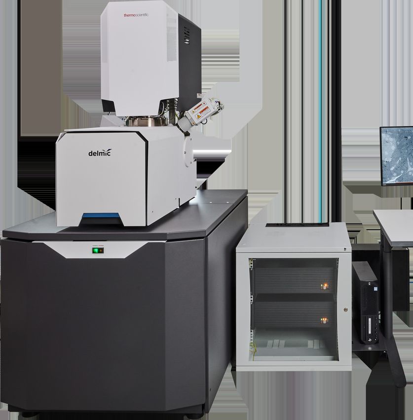
FAST-EM specifications sheet - Ultra-fast automated multibeam electron microscope - ELMI 2021
←
→
Page content transcription
If your browser does not render page correctly, please read the page content below
specification
sheet

     FAST-EM
     specifications sheet
     Ultra-fast automated multibeam
     electron microscope

                                      V01-01 2021-20-04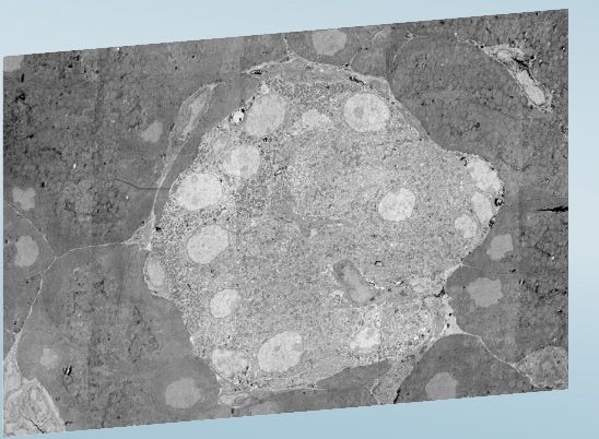
FAST-EM specifications sheet          Ultra-fast automated multibeam electron microscope

Introduction
FAST-EM is an ultra-fast automated multibeam electron
microscope (EM) designed to make complex and large
EM projects simple and efficient. Thanks to its automated
acquisition, this high-throughput system is ideal for imaging
large or multiple samples for quantitative analysis. Delivering
powerful insights while keeping the workflows simple, this
system allows users to shift their focus from microscope
operation to data analysis.

FAST-EM can be used to explore cell architecture, the
interaction of neuronal circuits, and the analysis of any
biological material. It is extremely beneficial for large volume
3D imaging, large scale 2D imaging and, in general, as a tool
that can significantly speed up daily microscopy work.

Key benefits

                                                                                             Achieve high sustained               Get the details and the big
              Image faster                              Focus on data analysis                                                             picture
                                                                                                  throughput
  High acquisition speed by using 64                 Leave the system to automatically   Minimize the overhead during imaging   Collect nanoscale detail while retaining
 electron beams and short dwell times                acquire complex datasets without           with robust automation               larger context of the sample
                                                           constant supervision

V01-01 2021-20-04                                                                                                                                                          1
FAST-EM specifications sheet Ultra-fast automated multibeam electron microscope
Workflow at glance
Image with 64 beams Enable shorter dwell times Automation software Load multiple samples at once
To achieve high-throughput imaging, The FAST-EM system uses Scanning Projects for FAST-EM are easily created and One of the aspects of EM workflows that
FAST-EM uses 64 electron beams. These Electron Transmission Microscopy (STEM) managed using robust automation and easy- introduces overhead into a project is sample
beams are scanned over the sample in for image formation. This is achieved by to-use software. exchange, which means that the operator
parallel, and signals are recorded using a fast placing samples directly on a scintillator has to supervise the system. FAST-EM allows
and highly sensitive Silicon Photo Multiplier screen. Scintillators produce localized The reliability of the microscope and the loading of up to nine substrates at the same
(SiPM) array. This approach achieves cathodoluminescence when struck by software allow the operator to leave the time, where each substrate can hold tens or
significantly higher acquisition speeds. electrons, which is captured using optical system running without constant babysitting. even hundreds of sections. This allows for up
microscopy. The resulting light is then to 72 hours of continuous imaging.
detected on the Silicon Photo Multiplier
(SiPM) array, and processed to form the final
gray-scale image.
V01-01 2021-20-04 2FAST-EM specifications sheet Ultra-fast automated multibeam electron microscope
System specifications
Electron optics
System base Thermo Fisher Scientific Apreo 2
Emitter: Schottky field emission source
Emitter stability: Per 24 hours 3%
High tension range: 2.5-10 kV
Beamlet current: 400-800 pA
Total current: 25.6-51.2 nA
Electron beam resolution: (35-65% edge) 4 nm
Nominal working distance: 5 mm
Single beam mode: Yes
Scanning and detection
Resin-embedded rat pancreas tissue imaged in FAST-EM.
Multiprobe arrangement: Square, 8 x 8 array Sample courtesy of Ben Giepmans’ lab (UMC Groningen)
Beamlets: 64
Dwell time: 400 ns minimum, adjustable
Pixel size: During field acquisition 4 nm
Field of view: At 3.2 μm pitch 25.6 x 25.6 um
Detectors Multibeam Transmission detector with 64 silicon photomultiplier cells
Single-beam Segmented in-lens backscattered electron detector
Upper in-lens secondary electron detector
Sample and stage
Type 3 axes motorized (XYZ)
Stage position readout Laser interferometry for nanometer-level positioning accuracy
Travel range XY 50 × 50 mm
Typical substrate size 14 x 14 mm*
Max simultaneous substrates When using 14 × 14 mm substrates 9 – for a total of ~850 1*1 mm sections
* Other sizes available
V01-01 2021-20-04 3FAST-EM specifications sheet Ultra-fast automated multibeam electron microscope
System specifications
Imaging workflow
Usable samples Directly on scintillators Resin sections (maximum thickness of 150 nm), nanoparticles, Contact information
vesicles, viruses
On TEM grids** Resin sections (maximum thickness of 150 nm), nanoparticles, DELMIC B.V.
vesicles, viruses Kanaalweg 4
Unattended run-time 72 hours 2628 EB Delft
Use cases Routine data collection Semi-automated imaging of user-defined ROIs and section arrays www.delmic.com
Sustained throughput During megafield acquisition at 100 megapixels/second info@delmic.com
400 ns +31 1574 401 58
Data format One 16-bit TIFF per field image, stored per project
Software
Microscope control Linux-based acquisition control
Acquisition support User guidance for basic operations
System health monitoring Continuous logging of crucial system features
Automatic calibrations Detector gain, detector alignment, autostigmation, autofocus,
global alignment of components
Vacuum and support
hardware
Vacuum pumps Turbomolecular pump, scroll pump (backing)
Operational vacuum ≤ 3 × 10⁻⁵ mbar
Network storage connection 10 Gbit Ethernet (10GBASE-SR using LC Duplex OM3 MM fiber)
Optional components
High performance storage module Scalable high-speed storage for data analysis and data sharing
Support Infrastructure Standalone water chiller
Acoustic enclosure for backing pump
Consumables 14 × 14 × 0.15 mm scintillator substrates
** Requires TEM grid mount
V01-01 2021-20-04 4You can also read