Functionalized graphene-based nanocomposites for smart optoelectronic applications
←
→
Page content transcription
If your browser does not render page correctly, please read the page content below
Nanotechnology Reviews 2021; 10: 605–635
Review Article
Suresh Sagadevan*, Muhammad Mehmood Shahid, Zhan Yiqiang, Won-Chun Oh*,
Tetsuo Soga, Jayasingh Anita Lett, Solhe F. Alshahateet, Is Fatimah, Ahmed Waqar,
Suriati Paiman, and Mohd Rafie Johan
Functionalized graphene-based nanocomposites
for smart optoelectronic applications
https://doi.org/10.1515/ntrev-2021-0043 electrical changes are important for many new technologies
received April 14, 2021; accepted June 14, 2021 based on switchable devices. As a two-dimensional smart
Abstract: The recent increase in the use of graphene and electronic material, graphene has received widespread
its derivatives is due to their exceptional physicoche- attention, and with that view, we aim to cover the various
mical, electrical, mechanical, and thermal properties as types of graphene oxide (GO)-based composites, linking
the industrial materials developed by involving graphene their optical and electrical properties with their structural
structures can fulfill future needs. In that view, the potential and morphological ones. We believe that the topics covered
use of these graphene-containing nanomaterials in electro- in this review can shed light on the development of high-
nics applications has encouraged in-depth exploration of yield GO-containing electronic materials, which can be
the electronic, conducting, and other functional properties. fabricated as the field moves forward and makes more
The protecting undifferentiated form of graphene has simi- significant advances in smart optoelectronic devices.
larly been proposed for various applications, for example, Keywords: graphene oxide, optical properties of gra-
as supercapacitors, photovoltaic and transparent conduc- phene oxide, graphene synthesis, functionalized gra-
tors, touch screen points, optical limiters, optical frequency phene, optoelectronic devices
converters, and terahertz devices. The hybrid composite
nanomaterials that undergo stimulus-induced optical and
1 Introduction
* Corresponding author: Suresh Sagadevan, Nanotechnology &
Graphene is exciting as the gateway to a new era in mate-
Catalysis Research Centre, University of Malaya, Kuala Lumpur
rials science and technology research because of its
50603, Malaysia, e-mail: drsureshnano@gmail.com
* Corresponding author: Won-Chun Oh, Department of Advanced ability to convert itself into many different forms with a
Materials Science and Engineering, Hanseo University, Seosan-Si, change of structure and dimensionality. Figure 1 shows
Chungnam 356-706, Republic of Korea, e-mail: wc_oh@hanseo.ac.kr the schematic representation of many different shapes of
Muhammad Mehmood Shahid, Zhan Yiqiang: Center of Micro-Nano graphene and their formation. The very supportive, flexi-
System, School of Information Science and Technology,
ble, and film-forming morphology of graphene allows for
Fudan University, Shanghai, 200433, China
Tetsuo Soga: Department of Electrical and Mechanical Engineering,
their wrapping, rolling, and can even be staking into
Nagoya Institute of Technology, Gokiso-Cho, Showa-Ku, zero-dimensional (0D) fullerenes, one-dimensional (1D)
Nagoya 466-8555, Japan carbon nanotubes (CNTs), two-dimensional (2D) graphene,
Jayasingh Anita Lett: Department of Physics, Sathyabama Institute or three-dimensional (3D) graphite, as shown in Figure 1
of Science and Technology, Chennai 600119, Tamil Nadu, India [1,2]. The graphene with its 2D carbon sheet maintains sev-
Solhe F. Alshahateet: Department of Chemistry, Mutah University,
eral other magical properties such as the thickness similar
P.O. Box 7, Mutah 61710, Karak, Jordan
Is Fatimah: Chemistry Department, Universitas Islam Indonesia, to that of a single-atom, large theoretical surface area,
Kampus Terpadu UII, Jl. Kaliurang Km 14, Sleman, Yogyakarta 55584, high conductivity at room temperature, and wider electro-
Indonesia chemical window [3]. In addition to those magical proper-
Ahmed Waqar: Institute of Advance Studies, University of Malaya, ties, the graphene nanosheets (NSs) can also serve as an
Kuala Lumpur 50603, Malaysia
excellent host material for the growth of high-performance
Suriati Paiman: Department of Physics, Faculty of Science,
Universiti Putra Malaysia, 43400, Serdang, Selangor, Malaysia
nanomaterials with enhanced electrochemical characteris-
Mohd Rafie Johan: Nanotechnology & Catalysis Research Centre, tics [4–7]. Such enhancing electrochemical characteristics, in
University of Malaya, Kuala Lumpur 50603, Malaysia particular, have the conductivity properties to significantly
Open Access. © 2021 Suresh Sagadevan et al., published by De Gruyter. This work is licensed under the Creative Commons Attribution 4.0
International License.
606 Suresh Sagadevan et al.
graphene, it can be transformed into distinctive forms, such
as quantum dots (QDs), nanoribbons, foams, and hydrogels
according to suitability [18,27–30].
Graphene is the parent of all graphitic forms of
carbon and is a monolayer of carbon atoms joined collec-
tively by a foundation of protruding sp2 hybrid bonds
[31]. The exceptional properties of graphene are derived
from the 2p orbitals of π-state bands; as a result, the
graphene inherits various characteristics, such as being
optically transparent and having better surface area,
excellent thermal conductivity, and mechanical proper-
ties [32]. These characteristics furnish graphene with a
significant dominance over similar materials used in
diverse industrial applications. Attributable to this, there
Figure 1: (a,b) Graphene is a 2D building material with its wrapped is always a rising demand for high-quality graphene in
(0D Buckyball’s), rolled (1D nanotubes), and stacked (3D graphite) vast quantities from both academia and industry to meet
forms. these increasing requirements and propel the material
into commercial domains. Since graphene’s discovery,
affect the sensitivity due to the high surface area and dense it has revolutionized the field of nanotechnology because
analyte molecules [8–11]. of its single-layered one-atom-thick flatbed structure [33].
In comparison to the CNTs, the graphene material not Up until now, many attempts have been made to synthesize
only possesses similarly stable physical properties but graphene at a large scale to fulfill the industrial demands, in
also is cheaper to produce along with the maintenance particular for industries that use graphene to produce state-
of more edges that particularly helps for the tuning of of-the-art composite materials; hence graphene changed
edge structure, especially the functional groups [12]. the global market dramatically. Since the discovery of gra-
Graphene has the properties of the theoretical spe- phene in 2004, it has stormed the field of nanotechnology
cific surface area of 2,630 m2 g−1, high intrinsic mobility with an exponential increase in its applications as it appears
of 200,000 cm2 V−1 s−1, high Young’s modulus ∼1.0 TPa, as a “magic bullet” on the horizon of the composite world.
thermal conductivity ∼5,000 Wm−1 K−1, optical transmit- The research related to graphene and graphene-based
tance ∼97.7%, excellent biocompatibility, and super-para- nanocomposites has generated many reports and that is
magnetism, which can expand its applications to several why Geim says that graphene research has reached unex-
fields [13,14]. The common applications include field- pected heights in the area of materials science [34].
effect transistors, functional devices (signal emission, Some of the pioneering research in the area of gra-
transmission, modulation, and detection), sensors and phene/graphene oxide (GO) includes reduced graphene
metrology, transparent conductive films (TCFs; can reach oxide (rGO)–cobalt oxide (Co3O4)@Pt nanocomposites
up to 97.7% in the near-infrared and visible region), clean for nitric-oxide sensors [10], GO–Ag nanocomposites for
energy devices (graphene-based electrodes for lithium-ion the detection of nitrite ions [35], Co3O4 nanocube-doped
batteries [LiBs] and electrochemical double-layer capaci- ChGP nanocomposites for methylene blue dye degrada-
tors), biomedical applications, optical electronics, compo- tion [36], rGO–Co3O4 nanocubes as an anode material for
site materials, catalysis (oxygen reduction reaction), and the direct methanol fuel cell [5], and rGO/Co3O4 nano-
photovoltaic cells [12,13,15–24]. composites for supercapacitor applications [37]. The
The origin of graphene was started 8 years after the discovery of 0D buckminsterfullerene [38], and shortly
award of the Nobel prize in physics and 14 years since thereafter 1D CNTs [39], has increased the interest of
the first report of monolayer graphene [25,26], where the research in carbon-based nanomaterials [40]. It is pro-
researchers’ attention to graphene-based magical compo- posed that fullerenes and CNTs are the derivatives of 2D
sites continued to the boom. The main attraction of gra- graphene sheets, which are viewed as the chief building
phene is the cross-functionality of 2D atomic crystals with block material for all other allotropes of carbon (Figure 1).
unique characteristics, and at the same time, 2D structure Similarly, graphite is made up of stacked sheets of gra-
sometimes creates hurdles in the exploitation using its zero- phene one on another maintaining the interlayer distance
gap semi-metal property. To overcome such limitations of (3.37 Å) [41]. Also, a section of graphene sheet can be
Graphene-based nanocomposites 607
virtually wrapped or rolled to make “fullerenes” and “CNTs” and one out of the three electrons per atom yields the
[42], but in reality, they are not derived from graphene. For bonds. The electrons are responsible for the electronic
the lab-scale production of graphene, numerous methods properties at low energies and form energy bands far
have been devised. These include the “scotch-tape method” away from the Fermi energy [56]. Graphene has sp2 hybri-
as the primary one [33] that can be adopted for the isolation of dization between S and P orbitals, which makes trigonal
pure defect-free graphene, followed by numerous other synth- planar structure by forming a bond between carbon
esis processes such as exfoliation methods [43–47], chemical atoms at 1.42 Å distance. The band between carbon atoms
vapor deposition (CVD) [44–49], pyrolysis [49], chemical strengthens the lattice structure of all allotropes. Out of
synthesis [50], arc discharge [50], unzipping of CNTs [51], many interesting properties, graphene has its low-energy
solvothermal [52], epitaxial growth [44], molecular beam epi- excitations massless, chiral, and Dirac fermions; more-
taxy [53], and electrically assisted synthesis [54]. As shown in over, at a neutral pH, graphene has the chemical poten-
Figure 2, the mechanical exfoliation of graphene results in the tials that cross exactly the Dirac point. The specific dis-
generation of pristine graphene (pure and unoxidized form) persion, which is possible only at low energies, imitates
in a bottom-up approach, while the chemical oxidation forms the quantum electrodynamic (QED) physics for massless
GO and further exfoliation and reduction ultimately produce fermions with only a difference of speed vF of Dirac
rGO in a top-down approach [55]. fermions in graphene, which is 300 times slower than
In this review article, we have focused on the recent the speed of light. Hence, graphene bears many of the
research including the synthesis and applications of gra- unusual properties of QED at smaller speeds (Figure 3)
phene-based nanocomposites. Though the special focus of [57–59]. As shown in Figure 5, graphene’s electronic
this article is on graphene and functionalized graphene-based orientation and its structure support for very high charge
materials for optical applications, it also provides an overview mobility. Still, for the long term, the mobility of graphene
of graphene synthesis (bottom-up and top-down approaches) is mostly limited to 2,000–15,000 cm2 V−1 s−1 and is
and its characteristics, since graphene is the main roll mate- because of the defect levels, microscopic ripples, and
rial of the current review article. scattering [33,60,61]. Furthermore, the clean surface-sus-
pended graphene has carried mobility up to the range of
200,000 cm2 V−1 s−1, and such suspended graphene can
reduce the scattering by making use of the substrate, and
2 Properties of graphene due to which the carrier mobility and ballistic transport
become possible. This ultrahigh mobility carrier enables
For the formation of strong covalent bonds, there are new provisions in the field of electronics and optoelec-
three electrons involved per carbon atom of graphene, tronics [62].
Figure 2: Schematic representation of the methods used for the synthesis of graphene, which is classified into top-down and bottom-up
approaches.
608 Suresh Sagadevan et al.
presence of light is shown in Figure 4a, and the graphene
material can absorb only 2.3% of its incident white light
with 97.7% transmittance [69]. The graphene has the
thickness of one atom, and the frequency of incident light
has no relationship with the intensity of absorption [26].
These exceptional characteristics result from the electrons,
conical band, and holes at the Dirac fermions in its sheets
[70]. However, the bilayer graphene can absorb white light
up to 4.6% and in accordance with the increase of the
number of layers, the absorption capabilities of graphene
also increase linearly. The individual layer absorption can
be obtained as A = 1 − T = πα = 2.3%, where α ∼1/37
represents the fine-structure constant [71]. So, with each
layer absorbing 2.3% of light and with a graphene sample
of five layers can have a total of 11.5% absorption and
88–88.5% optical transparency. Hence in a study, the
ultraviolet radiation spectrum in the wavelength range of
900–300 nm was used to identify graphene, where the
results proved that the graphene under these conditions
is featureless, and at the same time, the maximum absorp-
tion was noted for this material around 270 nm wave-
length, thereby confirming its optical properties at specific
regions [69].
Figure 3: (a,b) Electronic and optical properties of graphene; linear
energy dispersion of massless Dirac fermions (MDFs) in gra-
phene [63]. 2.2 Linear absorption
2.1 Optical properties The unique band structure of graphene has novel optical
properties, i.e., when incident light falls on the surface of
Graphene with its multilayer structure can absorb radia- graphene, the electrons are ejected from the valance
tion over a range of frequencies, and its ability to generate band and excited to the conduction band by absorbing
optical transitions in the electric fields is called gate- the photon energy. Thus, the conductivity caused by
dependent optical transitions [64–68]. The absorption photons in single-layer graphene depends upon the struc-
rate of mono- and bilayer ability of graphene in the tural constant as follows [63]:
Figure 4: (a) Absorption rate of mono- and bilayer graphene in the presence of light and (b) the dynamic simulation of graphene-saturated
absorption [73].
Graphene-based nanocomposites 609
down into a train of ultrashort pulses, which are the
key constituent of passive-mode locking (PML) in laser
cavities. Most of the materials need higher optical inten-
sities even closer to their optical-damage threshold,
at which they undergo SA [74]. In this phenomenon,
the mirrors used to operate in a narrow spectral range
need advanced fabrication methods, since they are not
very tunable. Recently, carbon-based nanomaterials have
proved themselves to be potential, cost-effective, and fea-
sible alternatives for developing next-generation PML
lasers. Graphene, as a carbon material, has played a
role in overcoming these limitations with its strange con-
Figure 5: Comparison of the UV-Vis absorption spectra of GQDs and ical band structure [75], giving rise to broadband reso-
surface functionalized GQDs [86]. nant SA even at remarkably low light intensities [76].
Moreover, graphene’s band structure can be further
tuned by applying an external voltage to the gate [77].
α = e 2 / 4πε0 ℏ ≈ 1/ 137. (1)
The PML ultrafast laser action, broadband adjustability,
Also, T is the linear transmittance of single-layer gra- and exchange quality factor are few of the properties that
phene and is represented as follows: can be accomplished using SA components prepared
using graphene to generate large energy pulses. Modern
T = 1/(1 + 0.5πα)2 ≈ 1 − πα ≈ 97.7%. (2)
theories have shown that the single-mode function of the
In the visible region, the reflectance of graphene is random laser is achievable by implanting graphene flakes
less than 0.1% and is counted as 2% for graphene with in the gain medium [78]. For this purpose, the single-
ten layers. Figure 4b represents the dynamic simulation particle MDF representation turns out to be a suitable
studies of graphene to explain its optical properties, and theoretical support [79].
from that, it can be inferred that graphene can absorb
light of any wavelength due to the zero bandgap [72].
Furthermore, the theoretical calculations also confirm
that graphene can absorb different bands of light at dif- 2.4 Luminescence
ferent configurations of QDs and substrate-based gra-
phene [49,50]. Graphene maintains its absorption rate Graphene has been used for photoluminescence and
of light even at weak incident light power when the electromagnetic transport applications because of its
energy band near the Dirac point of graphene is not filled. extraordinary characteristics and so has created a wide
It is observed that graphene cannot continue the absorp- range of research interests [80–83]. The fragmented gra-
tion of light to achieve sutural absorption because of phene and graphene-derived QDs (GQDs) present excep-
the Pauli blocking effect. It has a nonlinear absorption tional photoluminescence properties in the preparation
[51–56], and its saturable absorption (SA) coefficient can process and make graphene a photoluminescent material
be calculated as follows [51]: taking advantage of the coherence between π electrons
α∗(N ) = α∗S /(1 + (N / NS)) + α⁎NS, (3) that can be reduced by tuning its chemical and physical
properties. The oxidation plasma treatment of single-
where α∗S and α∗NS represent saturated and unsaturated layer graphene sheets can introduce bright light into it
absorption components, respectively, N is the photo- [80], and in the same way, the bulk graphene and dis-
induced electron–hole density, and Ns is the saturation persion can exhibit a large uniform area of photolumines-
density. cence [84,85]. A routinely prepared photoluminescent
graphene material can be used in sandwich form with a
conductive layer of graphene to make sandwich-type
2.3 SA light-emitting diodes (LEDs), which can operate with a
wavelength range of infrared to blue [80]. In general,
SA is a nonlinear occurrence consisting of the quenching G-QDs are synthesized using a blue-radiated hydrothermal
of optical absorption beneath high-intensity radiation. method [83]. Wang and his colleagues investigated the
Thus, the outcome of SA is a continuous wave broken photoluminescence mechanism in G-QDs [86] and found
610 Suresh Sagadevan et al.
that the excited-state transfer between electrons and
holes and the influence of edge-effect light luminescence
(as shown in Figure 5) made in visible photolumines-
cence devices within the scope of the preparation of a
theoretical basis.
With a decrease in the size of the QDs, graphene
exhibits quantum confinement and unique edge effects
[81–86]. A few other reports presented the photolumines-
cence of GO as recombination of e–h pairs of localized
states of the sp2 cluster [84]. The size or conjugate length
of the sp2 cluster is the major part that defines the energy
gap between π* and π [87], which is likely to be explained
by the edge effect of graphene and the defects related to
the oxidation process. Some reports say that photolumi-
Figure 6: (a–e)The energy levels of ideal graphene NSs and deco-
nescence in GQDs is the consequence of the radiative rated with various functional groups, such as atomic vacancy,
recombination of electrons at the graphene edges [88], hydroxyl, epoxy, and carboxyl groups [90].
by a transition in free zigzag sites instead of transition
between π* and π as defined previously. However, it
doesn’t matter which mechanism is used for photolumi- gap energy of ideal graphene clusters decreases. Based
nescence of GQDs, but it has the same characteristics; the on Gaussian and time-dependent DFT simulations, Chien
excitation wavelength is responsible for the changes in et al. found that these functional groups caused distortions
emission spectrum wavelength. Therefore, the organic in the aromatic rings and that these disorder-induced loca-
fluorescent material has a great influence in developing lized states caused absorption in the lower energy regions
cheap optoelectronic devices [89]. (Figure 6) [90].
Although the exact structure of GO is not well-under- Thorough investigation of the fluorescence difference
stood, there is a general agreement that the bandgap is between GQDs and graphene-derived GOQDs (GOQDs)
influenced by morphology sizes, oxygen coverage densi- will help in the in-depth understanding of their lumines-
ties O/C ratio, surface functionalities, and other factors. cence mechanisms. For example, Liu et al. have success-
As the size of GO NSs grows larger, the number of con- fully synthesized highly homogeneous GQDs and GOQDs
jugated aromatic rings increases, lowering bandgap energy. from the suspension of GO solution after sonication and
Upon conjugation with different functional groups, such as centrifugation [91]. Both GQDs and GOQDs had circular
atomic vacancy, hydroxyl, epoxy, and carboxyl groups, the shapes with a diameter of 4 nm, but GOQDs had different
Figure 7: (a) PL spectra and the corresponding fluorescent images of GQDs and GOQDs, (b) PL excitation spectra of GQDs and GOQDs with
varying detection emission wavelengths [91].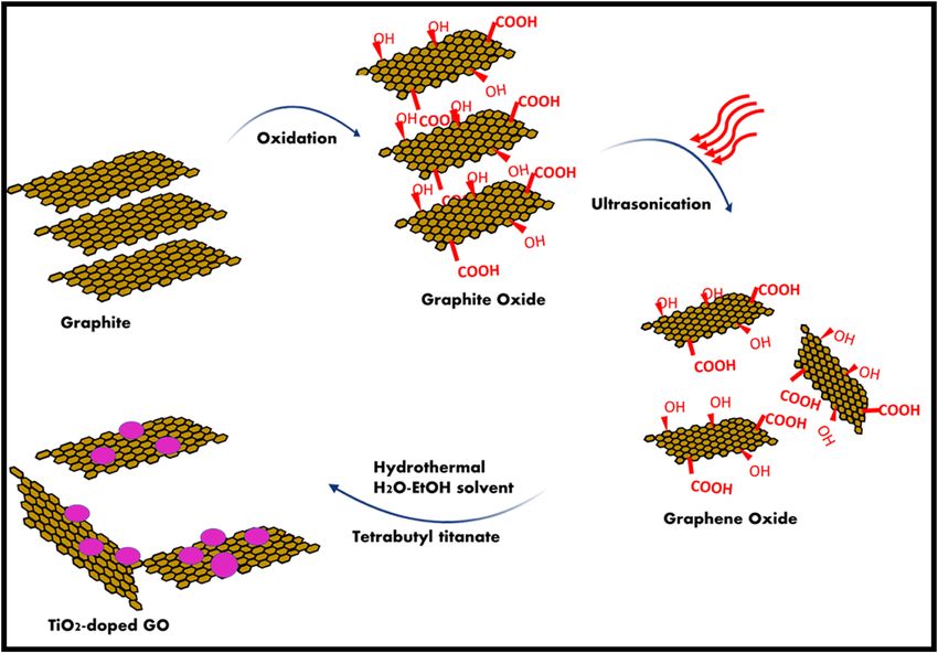
Graphene-based nanocomposites 611
Figure 8: Schematic illustration of GO-based all-solid-state electric double-layer transistor. G, S, and D denote the gate, source, and drain
electrodes [92].
oxygen-containing functional groups, while GQDs had a The mechanisms that explain the evolution of GO
pure sp2 carbon crystalline structure without oxygenous photoluminescence is shown in Figure 10. Figure 10a
defects. GQDs and GOQDs released transparent blue shows the original GO, which is made up of various dis-
(420 nm) and green color (480 nm) emissions, respec- order-induced defect states within the p–p* gap and has
tively, according to the spectral analysis, and the fluor- a large prominent PL spectrum centered at longer wave-
escence intensity of GQDs was about 3.5 times higher lengths. As shown in Figure 10b, the number of disorder-
than that of GOQDs, despite its concentration, which is induced states within the p–p* gap decreases after deox-
about 10 times lower (Figure 7a and b) [91]. ygenation, whereas the number of cluster-like states from
During the fabrication of graphene from GO NSs, newly formed small and isolated sp2 domains increases.
reductive treatment is often used to eliminate oxygen- At shorter wavelengths and with narrower bandwidth,
containing groups. Meanwhile, the bandgap structure electron–hole recombination among these sp2 cluster-
of GO NSs is evolving, resulting in a slew of new optical like states induces blue fluorescence. As a result of mod-
properties. For example, Eda et al. observed blue PL ifying the heterogeneous electronic structures of GO and
based around 390 nm for thin-film samples deposited rGO with variable sp2 and sp3 hybridizations by reduc-
from thoroughly exfoliated suspensions after exposure tion, the tunable PL spectra of GO are due to variance of
to hydrazine vapor [84]. The localization of e–h pairs the relative intensity ratios of PL emission from two dif-
was facilitated to radiative recombination by adequately ferent forms of electronically excited states [94].
regulating the concentration of isolated sp2 clusters
within the carbon–oxygen sp3 matrix via reduction treat-
ment, and the PL intensity could be increased ten-fold
compared to the as-synthesized materials. Furthermore,
it was found that the bandgap energy of GO NSs can be
continuously tuned by precisely regulating the reductive
extent, resulting in a variety of luminescent colors. The
bandgap of GO can be in situ and nonvolatile tuned by a
redox reaction using a solid electrolyte thin film by
simply applying direct current (DC) voltage inside an
all-solid-state device (Figure 8) [92]. The PL peak wave-
length can be adjusted from 393 to 712 nm by changing
the applied DC voltage between −3.5 and 2.5 V (Figure 9)
[93], where the polarity of voltage was defined as positive
when GO was oxidized and negative when reduced. A
wide emission peak at 676 nm was observed for pris- Figure 9: DC bias dependence of normalized PL spectra tuned by
tine GO. application of various bias voltages for 1,200 s [93].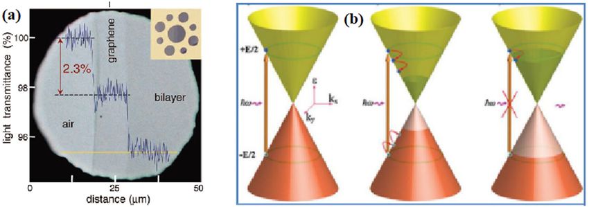
612 Suresh Sagadevan et al.
Figure 10: Proposed PL emission mechanisms of (a) the predominant IP1 emission in GO from disorder-induced localized states, (b) the
predominant IP2 emission in rGO from confined cluster states [94].
3 Synthesis approaches of method, graphite is generically exposed to a solution of
potassium permanganate, sodium nitrate, sulfuric acid,
graphene and water. During this process, the carbon scaffold is deco-
rated with 45% of oxygen functional groups (epoxy, car-
To synthesize graphene with different outcomes, there
boxyl, and hydroxyl). Since GO is an amorphous material
are different bottom-up and top-down techniques avail-
with a higher density of defects because of its intrinsic
able. The foremost route used for the synthesis of gra-
nature, it can be partially reduced to rGO by removing the
phene is direct peeling off graphite using scotch tape, but
oxygen functional groups (about 23%) using different routes.
this option will not work for the commercial production
The rGO, with a significant reduction of oxygen contents,
of graphene. The most famous bottom-up route is CVD for
performs electrically and thermally better than GO does, but
the production of a large-area continuous graphene film,
not like graphene, and is still considered to be amorphous
and this route comes under the category of bottom-up
[100]. In 2004, Novoselov et al. made several attempts to
because it incorporates the simpler molecules to form a
produce a single-layer graphene sheet [33,102,103]. These
continuous graphene film. Moreover, this method takes
efforts mainly involve the peeling of graphite crystals with
in hydrocarbon gas as a feeding stock and can result in
a specific limit using adhesive tape and transferring the
large-area polycrystalline films that are several square
thinned-out graphite onto an oxidized silicon wafer with a
meters in size [95,96]. Even though the CVD method is
thickness of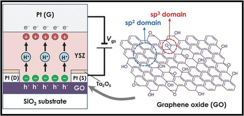
Graphene-based nanocomposites 613
Figure 11: Schematic representation of the formation of highly × rGO from graphite using the top-down approach.
The top-down approach is cost-effective and suffers from lateral force can also be applied by means of graphite’s
the limitations of large-scale production and quality con- self-lubricating ability in the lateral direction to promote
trol [104]. This approach generally involves the separa- the relative motion between two graphite layers (Figure
tion, peeling, cleaving, or exfoliation of graphite or its 12). These two mechanical routes are considered to be the
derivatives (GO and graphite fluoride) [105]. Usually, the prerequisites for the production of graphene by exfolia-
formulation of imperfection-free graphene with superior tion techniques. Moreover, the tailoring of these two
quality involves diverse techniques, such as mechanical routes could produce high-quality graphene with high
shedding of graphite, electrochemical peeling, sonication, efficiency [109]. Although the exfoliation process is a
surface functionalization, acid corrosion disintegration, destructive approach, the force generated by exfoliation
alkylation of graphene subsidiaries, chemical methods can also fragment large graphite particles or graphene
for aqueous/organically treated GO, thermal methods for layers into smaller ones (Figure 12) [110]. This exfoliation
shedding graphite, and chemical methods for the reduc- reduces the lateral size of graphene, which is not useful
tion of GO [55,105]. The production of graphene and its for accomplishing large-area graphene or for facilitating
nanocomposites by the peeling, surface functionalization, the exfoliation into smaller graphite flakes [109].
and chemical reduction with comprehensible strategies has
been extensively examined by Potts et al. [106]. Compar-
ably, Dhand et al. [107] have also investigated the synthesis
of graphene, elucidating several analogous approaches. A
diagram of the production of graphene by the top-down
approach is provided in Figure 11 [108].
A well-thought-out top-down scheme for extricating
mono-layered graphene flakes on the preferential sub-
strate is mechanical peeling. This technique is the prin-
cipally accepted strategy for the synthesis of graphene
flakes as it usually necessitates ∼300 nN μm−2 force to
detach a single atomic layer from graphite’s surface.
The piling up of sheets in graphite results in some mod-
erately enveloped π orbital, contradictory to the flat sur-
face of the sheet, and the attractive van der Waals force is
Figure 12: Schematic representation of the two kinds of mechanical
outstripped with the micromechanical chasm using the routes for exfoliating graphite into graphene flakes and the auxiliary
scotch tape to separate the graphite sheets [26,103]. A route for fragmentation.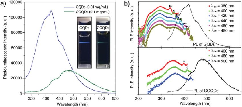
614 Suresh Sagadevan et al.
3.2 Bottom-up approach of graphene-accompanied electronics, such as high-frequency
electronics, light-emitting devices, and radiation hard devices
The deciding variables for the control of synthesized gra- [117]. Even though the abovementioned technique is very
phene’s morphology, crystallinity, and structure are the costly, taking into consideration the novel resistance stan-
tiny molecules of chemicals and catalysts within the dards located on the quantum Hall effect [118], top-gated
bottom-up approach, as in prior discussions [111]. In transistors have been made up of graphene on SiC [119].
the literature, the employment of hydrocarbons as a The high-frequency transistors have furthermore been
source of graphene has also been reported for the gen- uncovered with a 100 GHz cut-off frequency [120], superior
eration and use of metal-ion catalysts in the course of to the state of the art of Si transistors of similar gate
CVD practice [95,111–113]. In the CVD technique, the cap- length [121].
ability and strength to produce graphene layers are prob- During the year 2008–2009, the CVD emerged as an
ably tremendous, which makes this technique the most outstanding method for the fabrication and assembly of
acceptable one for the assembly and manufacturing of graphene because of its availability, first-rate quality
devices [111]. The assembling of graphite layers on a sili- [122], inexpensiveness, and applications involved in the
con–carbide substrate has been used since 1893 [114]. extensive fabrication of flexible crystal-clear conductors
Primarily, Van Bommel et al. in 1975 affirmed the growth for organic photovoltaic (OPV) cells and effectual tran-
of graphite on both 6H-SiC (001) substrates [115], and sistor production [123]. The graphene prepared by the
in the recent era, the technique has gained enormous CVD technique is more extensively intended for the fab-
importance because of the high-temperature sublimation rication of n-type graphene as compared to the scotch-
escalation deposition of mono-layer epitaxial graphene, tape method and can be fashioned in two uncomplicated
grown on the SiC substrate. One group has reported the steps, carbon atoms formed initially as a result of pyro-
depositing of mono-layers up to a few layers of graphene lysis of the precursor material and the disassociation of
deposits on the SiC substrates, mainly by means of high- carbon atoms to shape the carbon structure of graphene.
temperature (1,300–1,800°C) heating of SiC substrate The process is carried out in a high-temperature furnace
with the use of an ultrahigh vacuum or under an inert (1,000°C) in the company of a catalytic agent, where
atmosphere [114]. As the temperature required for the stress is created on the gas-phase surface of the transi-
sublimation of Si is less than that for carbon (∼1,500°C), tion-metal substrate (Ni, Cu, Co, Pd, Ir, Au, or Ru) and by
the SiC surface is given a thin layer of carbon [116]. The exposure to one of the hydrocarbons (methane, ethylene,
number of graphene layers stacked and blended onto the acetylene, or benzene) to form carbon layers. Further-
SiC substrate depends on the face orientation of the crystal more, the furnace is rapidly cooled to keep the precipi-
and layer growth conditions. Even though the most com- tated carbon layer from aggregating in order to form bulk
monly used epitaxial graphene growth surfaces are the hex- graphite in the course of chemical adsorption, thereby
agonal forms of 4H- and 6H-SiC substrates, the CVD gra- crystallizing into a contiguous graphene layer on the
phene growth has been achieved using the cubic 3C-SiC. metal substrates. Depending on the substrate quality,
In the modern era, the assembly of SiC wafers has precursor characteristics, width, and requisite structure,
become more aggressive because of the demand for epi- the various types of CVD processes, such as a thermal,
taxial graphene in the LED industry and in power elec- plasma-enhanced, cold wall, hot wall, or reactive type
tronics research. The epitaxial growth is the deposition of CVD, are usually employed [124].
a single crystalline film on monocrystalline substrate to
facilitate the epitaxial film. Thus, the fabrication involves
the deposition of high-crystalline graphene on single-
crystalline SiC substrates, either by means of homo- 4 Functionalization of graphene
epitaxial (film deposited on the identical substrate) or
hetero-epitaxial (film deposited on a dissimilar substrate) Different sorts of materials can be functionalized using
growth. In particular, during 2004, the SiC substrates graphene to actuate their effectiveness, which incorpo-
were primarily intended to measure parameters corre- rates atoms, nanoobjects, and polymers to form elec-
lated with the electrical measurements because of a tronic or photonic devices, with improved mechanical
wide-bandgap semiconductor (3 eV) on patterned epitaxial and thermal properties. Hence, the functionalized gra-
graphene [109]. One can anticipate that the epitaxial gra- phene nanocomposites can be crafted to attain altogether
phene growth technique on SiC might be an exceptionally significantly better performance than that of pure parti-
good technique for the large-scale assembling and marketing cles, nanoobjects, or polymers.Graphene-based nanocomposites 615
4.1 Functionalization with molecules charges of these biomolecules in the presence of water
stabilize the graphene sheets [129,130]. The molecular
One of the conventional and accepted ways to functiona- functionalization improves not only the solubility but
lize graphene is by using small molecules; for instance, also its optical efficiency. A better optical-limiting effect
surfactants, pyridine, protein, DNA, RNA, peptide, and was observed using porphyrin functionalized graphene
complex compounds, typically the anticancer drugs, can as compared to the criterion optical-limiting material
be functionalized on the graphene surface to upgrade and of C60 [131]. The electron/energy transport that exists
ameliorate the solution dispensation potential, optical, between the molecules of porphyrin and graphene was
electronic, and bio-related characteristics. Reconstructing partly responsible for this amazing optical-limiting effect.
the ability of graphene to dissolve in a wide range of sol- In another work, the non-covalent bonds and interac-
vents is one of the foremost critical purposes of graphene tions that exist between dendronized perylene bisimides
molecular functionalization. The chemically prepared gra- and graphene were accomplished in a homogeneous
phene possesses destitute solvency and is exceptionally solution, but the fluorescence of dendronized perylene
troublesome to be used in large-scale productions because bisimides was demolished as a result of the above inter-
of the difficulty of handling and complex procedures. As action [132]. The characteristics associated with biolo-
an illustration, sodium dodecylbenzene sulfonate can be gical molecules tend to be changed by functionalization
functionalized to modify the graphene surface as well as to with graphene. Specifically, the biomolecular functiona-
attain exceedingly soluble graphene over 1 mg mL−1 in lization of graphene tends to modify the bio-reactiveness
water, which makes possible solution-based fabrications while forming nanohybrids and nanocomposites. For
for the conductive film or any conceivable biological ana- instance, the single-strand DNA forming fusion with gra-
lysis [125–127]. An example of pyridine-based functiona- phene has a strong selectivity with the harmonizing DNA
lized graphene by Gupta et al. is shown in Figure 13 [128]. down to a single base mismatch [133]. In another work,
In order to achieve high solubility, the DNA and pro- the non-covalent authoritative and electronic intelli-
tein molecules are used to functionalize graphene as the gence between dendronized perylene bisimides and
Figure 13: Schematic representation of the synthesis of pyridine-based functionalized GOs [128].616 Suresh Sagadevan et al.
graphene was accomplished in a homogeneous arrange- semiconductors that are UV active possess a wider bandgap
ment, and the fluorescence of dendronized perylene that can improve the UV response of graphene when com-
bisimides was extinguished because of the formation bined with graphene/ZnO heterostructures [136]. Likewise,
of intelligent-hybrid composite structures [132]. The func- the TiO2 NPs confirmed superior photocatalytic and photo-
tionalization of graphene with that of organic molecules electrical activity when combined with graphene to form
and polymers changes the bio-related properties of nanocomposites [137]. Furthermore, in electrical and
graphene. electrochemical aspects, the graphene/nanoobjects exhibit
outstanding activity; one study observed that the MoS2
NSs/graphene nanocomposites showcased better electro-
catalytic characteristics than did pure MoS2 in a hydrogen
4.2 Functionalization with nanoscale evolution reaction [138]. Also, in studies related to electro-
objects chemical capacitors, Ni(OH)2, the NSs/graphene nanocom-
posites confirmed superior performance [139]. Similarly,
The functionalization of graphene heterostructures and the Co3O4 NPs/graphene nanocomposites exhibited much
nanocomposites with various nanoobjects, such as nano- better oxygen reduction than did a C/Pt catalyst, although
particles (NPs), nanowires, nanorods, and NSs, is another this activity was scaled down in pure Co3O4 NPs [140].
kind of functionalization that is often done. Based on the The metal NPs, exclusively Pt-functionalized ones with
intrinsic properties of materials, the nanoobjects are graphene, exhibit an exceptional electrocatalytic activity
endowed with various capabilities in contrast to pristine during methanol oxidization [141]. Figure 14 shows the
graphene. The nanoobject-based graphene nanocompo- functionalization of graphene with nanoscale objects by
sites particularly combine specific optical and electronic Shahid et al. [142].
properties to advance the possibilities of graphene in
numerous electronic and optoelectronic operations. Some
outstanding optical characteristics are exhibited by the
semiconductor nanoobjects that can overcome the low- 4.3 Functionalization with polymers
absorption behavior of pristine graphene. For instance,
the semiconductor CdS QDs/NPs have increased the An additional functional species extensively used to func-
photo-absorption along with photoelectrical responses tionalize graphene is the polymer to produce graphene-
appreciably when combined with graphene to form nano- based polymer composites. Generally, polymers resembling
composites [134,135]. Likewise, the ZnO nanowires/nanorod small molecules have also been functionalized to increase
Figure 14: A schematic representation of functionalized graphene with Co3O4 nanocubes and Au NPs.Graphene-based nanocomposites 617
the solubility of graphene. The amphiphilic conjugated tri- 5 Photonic and optoelectronic-
block copolymer has been functionalized to increase the
solubility of graphene in a variety of organic and inorganic
related applications
solvents [143]. Sulfonated polyaniline and amine-termi-
In general, to enhance the electron transport mechanism
nated polystyrene analogous to amine-terminated polymers
in optically active materials such as ZnO, TiO2, SnO2, etc.,
were initiated to be very successful in enriching the solubi-
the composite formation is the best suitable approach as
lity equally in organic solvents and water [144,145]. Exclu-
it can strongly influence the outer electron states and
sively in photonic and ultrafast photonic devices, graphene/
their movement. For example, in a study, Wang et al.
polymer nanocomposites have worked well [77,146]. Besides,
[149] investigated the optoelectronic properties of TiO2/
the optical absorption of the poly(vinyl acetate)/graphene
rGO nanocomposite sheets (with different graphene com-
nanocomposites was enlarged ten-fold times using only
position) formed by the hydrothermal method. During
0.07 wt% inclusion of graphene [146]. Also, some compar-
the synthesis, the reaction steps to undergo the conver-
able photonic effects were monitored using polyvinyl
sion of graphite into GO first and further to rGO with a 2:1
alcohol/graphene nanocomposites in mode-locked ultra-
ratio of water:ethanol blend in the presence of various
fast lasers [77]. Similarly, poly(3,4-ethylene dioxythio-
amounts of tetrabutyl titanate are represented schemati-
phene) (PEDOT)/graphene nanocomposites have also
cally in Figure 16. The investigation exhibited improved
increased the photoelectrical activity with an appro-
nonlinear optical (NLO) characteristics of a G0.25 nano-
priate percentage of graphene in the nanocomposite
composite associated with its components, which are
anode used as the LEDs [147]. Figure 15 shows the func-
endorsed by a blend of mechanisms. The function of
tionalization of GO by using functionalization of gra-
defect centers and electron/energy transport in the optical-
phene with polymers [148].
limiting action of G0.25 was verified using Raman and
Figure 15: Synthetic routes for achieving controllable functionalization of graphene [148].618 Suresh Sagadevan et al.
photoluminescent spectroscopies. Also, the intensity-depen- 5.1 Photovoltaic cells
dent exchange between reverse saturable and SA actions
with G0.50 nanocomposite was monitored. Yin et al. [141] built transparent and conductive elec-
An in-depth analysis reveals that a noteworthy fluor- trodes to be used for flexible OPV appliances (schemati-
escence quenching has been experienced for all the gra- cally represented in Figure 17) by coating the chemically
phene nanocomposites as compared to TiO2, thereby sig- synthesized rGO over polyethylene terephthalate sub-
nifying the occurrence and enhancing of the energy strates. The efficiency of OPV appliance chiefly relies on
transport mechanism due to the composite formation. the charge-transport effectiveness when the optical trans-
To optimize the NLO activity, the NLO absorption char- mittance of rGO is higher than 65% [142]. On the other
acteristics and optical-limiting reactions of nanocompo- hand, for lesser transmittance, the efficiency of OPV
sites were investigated using the Z-scan approach at a appliances is controlled by the light-transmission effi-
wavelength of 532 nm with 4-ns laser pulses using an ciency, i.e., the transparency of rGO films [150]. Following
optimal concentration of TiO2 in nanocomposites. The the application of about a 2.9% tensile strain on the fab-
superior NLO activity was monitored in G0.25 nanocom- ricated OPV device, the device can sustain for thousands
posite, in the nanosecond regime, and can be qualified as of bending cycles [151], thereby demonstrating for the
a result of the blended NLO mechanism, although the highly flexible properties of rGO films, and thus indicating
intensity-dependent actions in G0.50 were caused by the the potential applications of these materials toward flex-
mutual contribution from ESA and TPA. Overall, these ible optoelectronics applications.
conclusions demonstrate that TiO2/rGO nanocomposites A study by Şahin et al. [152] synthesized GO using the
with adequate TiO2 content can provide optical control Tour method and further tailored it with various amine
and NLO switching and thereby theoretically allow the sources (dihexylamine [DHA] and 2-ethylhexylamine [2EHA])
opportunity of ultrafast NLO candidates for photonic and involving various branched alkyl chains. The GOs and mod-
optoelectronic uses. ified GOs (mGOs) were used to investigate the efficiency of
Figure 16: Illustration of the fabrication process of TiO2-decorated rGO nanocomposite.Graphene-based nanocomposites 619
perovskite solar cells by using them as a buffering layer. The
mechanism of formation (represented in Figure 18) shows the
customized solar cells with the supplementary coating of
mGO derivatives sandwiched between the perovskite and
hole-transporting film exhibiting the overall efficiency better
than that of the reference cell [152]. This improved perfor-
mance may have resulted from the improved carrier transport
via the mGOs. To be specific, in general, there was a 10%
overall performance boost of the solar cells in solar-cell appli-
ances whenever GO customized with 2EHA was used, as com-
pared to the standard cells used devoid of the modified buffer
layer [152]. Figure 18: Schematic of the mechanism proposed for the binding of
It can be seen from the investigation that the mGOs, DHA and 2EHA onto the GO.
when functionalized as a buffer layer in the mixed
halide CH3NH3PbI3−xClx mesoporous perovskite solar
CoS/rGO, GO/SnO2, and so on, and this suggests the
cells, exhibited better characteristics than did with the
importance of incorporating graphene with other metal
reference appliance [153]. This improvement in character-
oxide NPs to enhance the photocurrent in solar cells
istics using the mGO coating resulted from the arrange-
[154–156].
ment of a homogeneous porosity observed in mGO film
that possibly made way for the holes transport and
thereby assisted the reducing charge recombination.
Moreover, the hydrophobic behavior exhibited by mGO 5.2 Electrochemical sensors
derivatives proved to be an additional shield to perovs-
kite films that protected them from humidity, air, and Taking into consideration of the fast-moving ability of
therefore escalated the stability of manufactured PSCs. graphene-based composites, Eshlaghi et al. [162] generated
Table 1 summarizes the various parameters that are sui- a sensor by integrating the GO surface [GO-imi-(CH2)2-
table for photovoltaic applications by making use of NH2] with the well-designed imidazole-(CH2)2-NH2 group.
functionalized graphene nanocomposites. From the com- This increases the surface area and conductivity of the
parison of data, it can be observed that the Fe3O4–rGO composite that can be used for reasonable and sensi-
composite has the superior photocurrent, followed by the tive recognition of Pb(II) in aqueous media (the whole
Figure 17: Schematic representation of (a) layer structure and (b) energy level for the OPV device, which is rGO/PEDOT:PSS/P3HT:PCBM/
TiO2/Al, with rGO as the transparent electrode [141]. PSS: poly (styrene sulfonate).620 Suresh Sagadevan et al.
Table 1: Comparison of the various parameters of photovoltaic properties of functionalized graphene nanocomposites
S. no. Counter electrodes Electrode JSC (mA cm−2) RS (Ω cm2) VOC FF ɳ (%) Ref.
1 rGO@PPy Counter electrode 7.49 — 0.70 0.42 2.2 [157]
2 CoS/rGO Counter electrode 19.42 16.05 ± 0.02 0.76 0.63 9.3 [154]
3 ZnO/rGO3 Photoanode 3.02 — 0.64 0.60 1.5 [158]
4 ZG + RB Photoanode 1.60 — 0.70 0.53 1.5 [159]
5 Fe3O4–rGO Counter electrode 24.45 — 0.75 0.32 5.9 [155]
6 Fe3O4–rGO Counter electrode 13.74 7.22 0.77 0.63 6.6 [160]
7 MoS2/graphene Photoanode 15.82 — 0.82 0.71 8.9 [161]
8 GO/SnO2 Photoanode 16.67 — 0.77 0.65 8.3 [156]
Jsc, short circuit current density; RS, series resistance; Voc, open circuit voltage; FF, fill factor; ɳ, efficiency.
synthesis route is provided in Figure 19). The character- technique fabricated a flexible TCF having the morphol-
ization of the composite cleared the favorable synthesis ogies similar to reinforced concrete, i.e., sandwiched the
strategy of the GO-imi-(CH2)2-NH2-CPE (conductive polymer single-walled carbon nanotubes (SWCNT) between PED-
electrode) grafting functional surface that can be used as a OT:PSS and polydopamine-functionalized rGO (PDA-rGO),
dependable Pb(II) sensor. Depending on the ideal conditions, and the formed structure is expected to have enriched
the Pb(II) calibration diagram recorded linearly (−0.58 V) performance in the LED devices (the whole structure of
within the concentration range of 5.0–300.0 nM, and the final composite is schematically represented in Figure 20).
high surface area and the solid Pb(II) adsorption capability Mussel-inspired PDA was popularized as a GO-reducing
with the good conductivity of the changed electrode sug- agent and modifier since the produced PDA–rGO was found
gested a reasonable Pb(II) detection limit of 0.30 nM. The to increase the interfacial bonding of sandwiching between
electrode provided ease –NH2 groups incorporating Pb(II) the conductive coating layers and the substrate surface,
with good reusability up to five times and reproducibility of which is a successful post-synthesis technique used for
approximately 90%, which is satisfactory for electrochemical the hybrid film to attain improved conductivity. The elec-
sensors. trode prepared by this method reported a low sheet resis-
Similarly, Wei et al. [163] used an rGO/SnO2/Au com- tance of 52.2 Ω sq−1 along with improved optical transmit-
posite for the electrochemical sensing of formaldehyde tance of 88.7% at 550 nm. Moreover, these transparent films
(HCHO), and its characterization revealed the formation displayed long-standing stability with comparatively low
of unique SnO2 NSs decorated with Au NPs that are roughness (about 2.41 nm), and its architecture maintained
homogeneously attached to the rGO’s surface. On testing, its flexibility throughout its bending course.
the gas-sensing analysis proved that the incorporation of In a similar study, the composite film using PDA-
SnO2 NSs with Au NPs and rGO improved the gas-sensing for rGO/SWCNT/PEDOT:PSS is formed to have applications
HCHO in terms of lower operating temperature, high sensor as organic LEDs, where the device luminance is measured
response, and good selectivity. The improved sensing prop- to be 2,032 cd cm−2 at 15 V, the maximum current efficiency
erties could mainly be attributed to the synergism of the of 2.13 cd A−1 at 14 V, thereby confirming for the presence
ohmic contact between rGO and SnO2 NSs, high surface of strong potentials that are especially applicable in flexible
area, and strong gas-adsorption capacity of sheet-on-sheet electroluminescent and photoelectric devices. Furthermore,
heterostructure architectures and the catalytic effect of Au Table 2 provides information about the various parameters
NPs. Finally, the work suggests that the rational design of 0D and applicability of nanographene and its composites for
noble-metal NPs, 2D metal oxide NSs, and 2D rGO form the LED devices.
ternary composites that provided an opportunity for the
achievement of high-performance sensing materials.
5.4 Optical and fiber-based biosensor
probes
5.3 Light-emitting and conducting diodes
To test the efficacy of graphene-based composite bio-
For exploring the LED properties of GO-based compo- sensor probes, Xu et al. [170] promoted a label-free glu-
sites, Wang et al. [164] with the use of spray coating cose biosensor that was effectively established andGraphene-based nanocomposites 621 Figure 19: Schematic of synthesis process for the functionalized (GO-imi-(CH2)2-NH2). planted based on the long-period fiber grating (LPFG) sensor has an excellent linear response even in the functionalized GO-glucose oxidase (GOD) by means of 0–1.2 mg mL−1 low concentration range with a sensitivity chemical crosslinking (schematic of the biosensor con- of ∼0.77 nm mg−1 mL−1. At the same time, the sensor struction is provided in Figure 21). Thus, the synthesized showed a faster and shorter response time of 2.16 s. GO-coated LPFG surface is an ideal candidate for che- Furthermore, based on the selectivity and sensitivity of mical and optical fiber sensing, because of the sensor’s the developed detector, it can be confirmed that the excellent operational environment, which can immobi- developed biosensor can be used to detect practical sam- lize GOD by copious binding sites because of the con- ples in the pharmaceutical research and medical diag- structive grouping of its remarkably large surface-to- nosis fields. volume ratio. It was found that gluconic acid and H2O2 In a different study [171], the GO–ZnS (GOZS) nano- were produced not only because of the major differences composite was successfully prepared by a solvothermal in the surrounding refractive index but also because of the method (synthesis route for the composite formation is reaction between GOD and glucose that leads to an obvious provided in Figure 22), where the characterization indi- shift in the LPFG transmission spectrum. The optimum cated for the even distribution of ZnS particles (20 nm conditions of the sensory system include a 4 mg mL−1 diameter) onto the surface of GO that supported for an GOD concentration and a solution pH of 7, where the increase in the nonlinear absorption and optical limiting Figure 20: Schematic illustration of TCFs with ultra-adhesion, relatively low roughness, and excellent electrical conductivity.
622 Suresh Sagadevan et al.
(OL) action of GOZS under ultrafast (1,030 nm, 340 fs)
[168]
[166]
[169]
[167]
[165]
Ref. excitation. The calculated theoretical values of the non-
linear coefficients (at 20.8 GW cm−2) of GO, ZnS, GOZS
Brightness (Cd m−2)
(4:5), GOZS (2:5), and GOZS (1:5) are 27.6, 25.4, 554.9,
193.3, and 117.1 cm GW−1, respectively. Based on the
39,000 Z-scan open-aperture investigation, the nonlinear activity
20,300
6,000
elevated nearly 5- to 22-fold in GOZS as compared against
798
pure GO and ZnS and is a result of the three-photon
—
absorption of the sample. Moreover, the homogeneous
Bandgap
250 meV
delivery of ZnS NPs on the GO’s surface increased their
surface area as well as their dispersibility and conse-
—
—
—
—
quently increased its light-absorption capacity. Further-
Particle size
more, the conjugated structure of GO along with the 2D π-
Up to 1 μm
electron permits the composite to generate additional
30 nm
10 nm
delocalized electrons. An improved absorption of free
—
—
Table 2: Comparison of various parameters (emission, quantum efficiency, etc.) of graphene and its functionalized nanocomposites
carriers and nonlinear activity was experienced, because
Quasi-core–shell QDs
the electron transport between GO layers and ZnS NPs
Hexagonal ZnO NPs
Graphene sheets
inhibited the recombination of free carriers, as well as
all these parameters, reinforcing the ability to organize
Morphology
it as an optical-limiting material.
NSs
—
Quantum efficiency (%)
5.5 Optical limiters
To test the efficacy of the charge transfer approach
on optical properties, the three kinds of porphyrin–GO
nanohybrids developed from the covalent functionaliza-
0.22
0.18
6.7
tion method by Chen et al. [172] such as TPP-GO, TTP-GO,
—
1
and TPP-GO-TTP are investigated to possess superior
Blue (λ ∼450 nm) to Red (λ ∼750 nm)
NLO absorption and OL characteristics. The effective
charge transfer from the porphyrins to the nanohybrids
of GO (schematic of its structural formation is provided
in Figure 23) was confirmed by the Raman spectroscopy
Emission wavelength
and other photophysical measurements. Also, within the
three GO derivatives tested, the ternary hybrid of TPP-
Green (450 nm)
GO-TTP has exhibited superior NLO properties as com-
pared to the other two and thereby emphasizing the
Green
Green
importance of fine-tuning the photophysical and optical
White
properties of nanohybrids through the introduction of
porphyrins. Furthermore, the results generated from this
PLEDs with a 4.3 nm thick GO
ZnO NP–rGO nanocomposite
study are potentially useful for the designing and devel-
opment of various GO-mediated porphyrin derivatives that
MoS2–GO composites
have applications in the NLO devices.
In a similar study [173], the nanocomposite of (3-amino-
propyl)triethoxysilane (APTES) functionalized multi-
semi-rGO
Material
layer GO and its incorporation within the organosiloxane
GQDs
matrices formed by the sol–gel method (sequential synth-
esis is shown in Figure 24) are observed to maintain better
S. no.
NLO and optical-limiting properties than that of their GO
precursor. Such an observed activity of GO–organosiloxane
4
2
3
5
1You can also read