High efficient heat dissipation on printed circuit boards - beam ...
←
→
Page content transcription
If your browser does not render page correctly, please read the page content below
RF & Wireless
High efficient heat dissipation on printed
circuit boards
The PCB by its nature is not a
good thermal conductor. It is
made of substrate materials that
are insulating electrical inter-
connections between compon-
ents. The thermal conductivity
of a typical substrate material
is about λ ~ 0.2 W/mK. Howe-
ver, copper, the material of the
conductive traces of a PCB, has
a high thermal conductivity of
λ ~ 390 W/mK. Depending on
the copper distribution the heat
flux in a printed circuit board is
normally better in the x-y plane
compared to the heat flux in the
z-axis (Figure 1).
A power or ground plane has a
bigger influence on the heat flux.
The heat flux and direction is
Figure 1: Heat flux in a PCB mainly dominated by the ther-
mal conductivity of the materi-
Abstract Introduction als and the ∆T in a given area.
This paper describes various Controlling the heat loss of The conductive traces of a PCB
techniques for dissipating heat electronic and microelectronic in practise cannot be used as a
from heat generating electrical systems is a more and more chal- good and efficient thermal con-
components on printed circuit lenging task as miniaturisation ductor. Their cross sectional area
boards (PCBs). Small copper is increasing, and the growth in is simply much too low.
coins that are matching the shape functionality is driving the com-
of the electrical components are Many microelectronic compon-
ponents to their limits, which ents are designed with a prede-
located underneath the compo- means that they are generating
nent and are integrated into the termined thermal pathway inside
more heat loss. Printed circuit their packages (Figure 2).
PCB construction. The heat from boards are the carrier of the com-
the component will be dissipated ponents and are therefore also The thermal loss of a plastic ball
by the copper coin to a heat sink highly involved in the matter of grid array (P-BGA) for example
or cold plate. The thermal con- controlling the heat. is dissipated via the base of the
ductivity of such kind of copper
coin is about 10 times higher
than usually achieved with so
called thermal via arrays. Several
different methods of integrating
copper coins into the construc-
tion of PCBs have been develo-
ped and will be discussed.
New developments such as the
“Chip-on-Coin” technique are
providing solutions for highly
miniaturised electronic circuits
and micropackaging. The inte-
gration of copper coins into
PCBs is suitable for all com-
mon substrates including RF and
microwave substrates as well as
Markus Wille for conventional PCB substrates.
Schoeller Electronics Systems (Key words: PCB, heat dissipa-
GmbH tion, thermal via, copper coin,
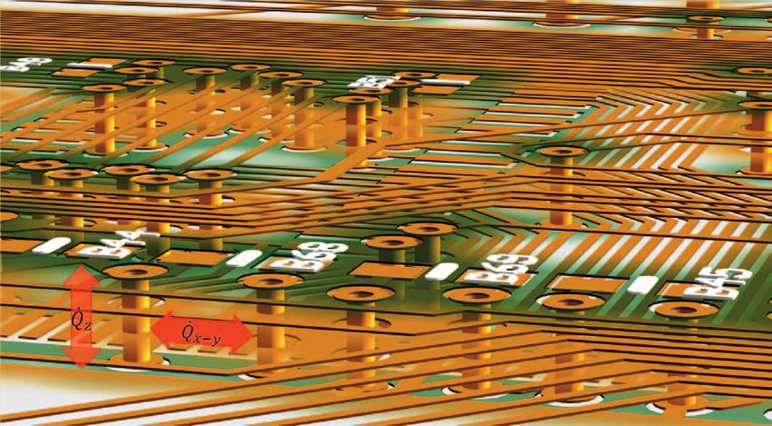
www.schoeller-electronics.com press-fit, bare die attach.) Figure 2: Thermal pathway inside component packages
74 hf-praxis 1/2018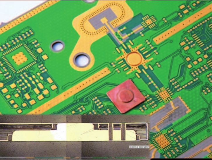
RF & Wireless
Figure 3: Thermal vias in a PCB
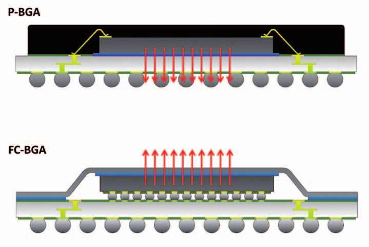
package whereas in a flip chip Local Heat Dissipation
ball grid array (FC-BGA) the By Copper Coins
thermal loss is guided to the top
surface of the package. To create a much more efficient
path for heat dissipation the idea
The principle that the thermal is to replace the arrangement of
loss of a component is transfer- thermal vias by some piece of Figure 4: PCB with press-fitted copper coin
red to the base of the package solid metal to increase substan-
provides the ability to integrate tially the amount of conductive appropriate openings of printed the normal fabrication process
a path for heat dissipation into material of thermal via arrays. circuit boards. The openings can has been finished. The copper
the physical construction of a be plated or non-plated. After the coins are bonded to the PCB in
printed circuit board. The goal was to find methods coin insertion the normal pro- defined locations by using ther-
and techniques that are com- duction process flow continues. mally and electrically conductive
A very common approach is to patible to the constructions and Figure 4 shows a segment of a film adhesives (Figure 5).
place an arrangement of vias the manufacturing processes printed circuit board with press-
as so called thermal vias in the of printed circuit boards and fitted copper coins. The copper coin in Figure 5 has
PCB underneath the component that are suitable for any assem- a flange the spreads the heat and
(Figure 3). bly processes. The material of The copper coin is designed with enables a better thermal connec-
choice is copper because of its a number of specific ribs along tion to a heat sink or cold plate
The base of the component is
high thermal conductivity and its the outer peripheral surface by enlargement of the effective
connected to the thermal vias on
excellent compatibility to PCB helping to control how strong surface area. It also carries the
the top side of the PCB. The heat the coin is fastened in the cut- adhesive preform (grey colour).
production processes.
flux is transferred through these out of the printed circuit board.
vias down to the bottom side of Several methods have been The ribs are also maintaining the The bond strength of the bon-
the PCB and then coupled into developed: electrical connection between ded copper coins depends on the
the heat sink or a cooling plate. • press-fitted copper coins, copper coin and PCB, e. g. the adhesive used, the type of sur-
For heat spreading the thermal grounding. faces, and also on the size and
vias are sometimes connected • adhesive bonded copper coins, geometry of the bonded area.
to power or ground planes of • embedded copper coins. Adhesive bonded
the PCB. Depending on the selected adhe-
All these methods are using copper coins sive the coin can be thermally
This principle is widely used at solid pieces of copper that are Another method is to attach the and electrically connected to
nearly any extra charges because integrated into the mechanical copper coins onto the PCB when the PCB or insulated or only
PCBs consists of lots of lots of construction of the printed cir-
vias anyway. The question is cuit board during its origin pro-
how efficient are thermal vias? duction process.
They may work fine for many
applications but the effective Press-fitted copper
thermal conductivity of ther- coins
mal vias is low due to the small
amount of conductive materials The insertion of copper coins in
that are involved. The heat flux printed circuit boards by means
flows mainly only through the of the press-fit method is a very
very small cross sectional area cost effective technique that
of the copper plating at the hole is practised e. g. on PCBs for
wall of the vias. The centre of engine controls in the automo-
the vias remains usually open tive industry or for power ampli-
and unfilled, and the surroun- fier in base stations of wireless
ding material is the substrate networks.
material of the PCB which is a Copper coins are pressed in an
good insulator. intermediate production step into Figure 5: PCB with adhesive bonded copper coin
hf-praxis 1/2018 75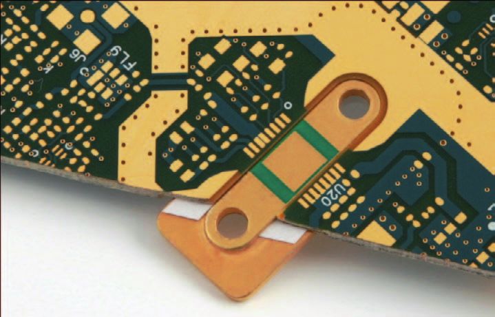
RF & Wireless
Thermal via array, 5 x 5 mm, via diameter = 0.5 λ W / R t h
mm, PCB: 1.5 mm thick FR-4 mK K/W
Vias plated with 25 microns thick Cu 14.5 4.1
Vias plated with 27 microns thick Cu 15.6 3.8
Vias plated with 30 microns thick Cu 17.2 3.5
Vias (25 microns thick Cu) filled with conductive 15.4 3.9
Silver paste
Vias (25 microns thick Cu) filled with solder 25.2 2.3
Vias filled with copper 75.9 0.8
for comparison: 1 copper coin, Ø 4 mm 194 0.3
Table 1: Effect of via filling
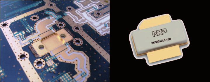
The copper coin of Figure 7 reduce physical space (minia-
includes a cavity in which the turisation) and therefore impro-
Figure 6: PCB with embedded copper coin flange of the power transistor ves signal performance (signal
will be placed for assembly. integrity) and speed. But it also
thermally or only electrically nique of the three described The design of the cavity mat- eliminates the package of the die
connected. methods in this paper. Howe- ches perfectly to the shape and which could be used for a new
ver, the press-fitting technique design of the flange. The depth approach for heat dissipation: the
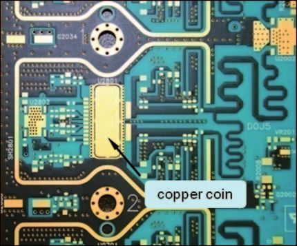
Embedded copper is limited to a maximal size of of the cavity is designed in such Chip-on-Coin technique.
coins approx. 40 mm x 40 mm to avoid a way that the flange is fully
overstressing the PCB with a too captured while the leads of the The bare die is attached directly
If the copper coin is integra- high mechanical load during the power transistor are aligned on a copper coin of the printed
ted into the construction of the press-fitting process. Therefore, straight over the solder pads of circuit board. The elimination
printed circuit board at the same the two other methods can be the PCB for best performances. of the housing of the die pro-
time and with the same process seen as back-up solutions for This method provides the oppor- vides an advantage for the heat
when all other layers of the PCB the case that press-fitted copper tunity to assemble such power dissipation compared to con-
are laminated together then this coins are not the best suitable devices in an automated process ventional housed components
method is called embedded technique for a specific appli- directly onto the PCB without the because some thermal bounda-
copper coin. Window cuts are cation. need of some manual operation. ries are removed from the ther-
prepared into the cores and prep- Cavities can be designed into mal pathway. The lower number
regs of a PCB stack and when the any of the copper coin methods of thermal interfaces in the ther-
stack-up construction is assem- Further Designs And
described in this paper. mal pathway leads to a reduced
bled prior lamination the copper Developments overall thermal resistance and
coins are placed into the window to a much higher efficiency in
cuts. The embedded copper coins Copper coins with Chip-on-Coin
the heat dissipation of the chip.
can be electrically connected to cavities The latest development on Compared to components in
the PCB by plated through holes copper coin technology is packages the junction tempera-
and galvanic copper deposition Some high power transistors are addressed to bare die attachment. ture falls. The mismatch of the
on the surface layers (Figure 6). housed in packages with metal The well known chip-on-board thermal expansion between the
flanges for heat spreading and technology (COB) is used to copper coin and the substrate
The embedded copper coin is
dissipation. They are normally
fully integrated in the layer
soldered or bolt down on heat
construction and lies flush in
sinks or cold plates. The copper
plane on both sides of the prin-
coin technology provides a solu-
ted circuit board.
tion to assemble such devices
The press-fitting of copper coins directly onto a printed circuit
is the most cost efficient tech- board (Figure 7).
Figure 7: Press-fitted coin with cavity Figure 8: Chip-on-Coin technique
76 hf-praxis 1/2018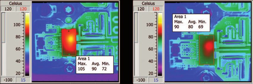
RF & Wireless

                                                                                                            the effect of filling the vias in
                                                                                                            the thermal via array (Table 1).
                                                                                                            The centre of the vias can be
                                                                                                            filled to enhance the thermal
                                                                                                            conductivity by replacing the
                                                                                                            air with some material of better
                                                                                                            thermal conductivity. They can
                                                                                                            be filled with conductive Silver
                                                                                                            paste which increases the ther-
                                                                                                            mal conductivity only slightly.
                                                                                                            That small gain in thermal con-
                                                                                                            ductivity could also be achieved
Figure 9: left: thermal vias, right: copper coin                                                            when a few microns of additional
                                                                                                            copper are plated into the vias.
material of bare dies can be com-     To illustrate the performance ofFigure 10. Both fields are same in A filling of the vias with some
pensated by replacing copper          copper coins versus thermal via size, 5 x 5 mm. The thermal via kind of solid metal such as sol-
with some material compositions                                       array consists of 25 vias with a der or copper results in a much
                                      arrays we can calculate the ther-
that are better suited for direct     mal conductivity and the thermaldiameter of 0.5 mm and a copper better thermal conductivity if a
die attachment such as Tungsten-      resistance.                     plating thickness of 25 microns void-free filling can be achie-
Copper or Molybdenum-Copper.                                          in the vias. The copper coin has ved. However, via filling with
                                  The effective thermal conduc-
An example of the Chip-on-Coin                                        a diameter of 4 mm.                   electrolytic deposited copper
                                  tivity λeff 1 and the thermal resi-
technique is shown in Figure 8.                                                                             in mass production is currently
                                  stance Rth 1 of a thermal via array The thermal conductivity of the
An arrangement of bare dies is                                                                              only feasible at a low aspect
                                  can be calculated with the fol- thermal pad with the copper
attached on a coin that is inte-                                                                            ratio (typ. 1:1), e. g. for micro-
                                  lowing equations:                   coin is λeff 2 = 194 W/mK and vias. In whatever way via filling
grated into the PCB construction.
The dies are connected with the                                       for the thermal via array we get is applied it will not reach the
PCB by wire bonding.                                                  the result of λeff 1 = 14.5 W/mK. performance level of the copper
                                                                      Assuming a PCB thickness of coin method.
Thermal Vias Versus                                                   1.5 mm we get a thermal resi-
                                                                      stance for the thermal pad with Reliability
Copper Coins                      and for a thermal pad with
                                                                      copper coin of Rth 2 = 0.31 K/W
                                  copper coin λeff 2 and Rth 2 in a
The better efficiency of copper                                       and for the thermal via array For PCBs with copper coins it
                                  similar way:                                                              is necessary that the coins are
coins compared to thermal via                                         Rth 1 = 4.14 K/W.
arrays can be analysed with ther-                                                                           integrated into the PCBs with
mographic images (Figure 9).                                          It can  be seen   that  the thermal   a high level of mechanical pre-
                                                                      conductivity of the thermal pad cision to meet specific parame-
Figure 9 shows two thermogra-                                         with a copper coin compared to ters and specifications such as
phic images of the power tran-                                        a thermal via array is more than flatness requirements for QFN
sistor stage shown in Figure 4.                                       10 times higher, thus the thermal components as an example. Also
In the left hand image the power Where                                resistance of the copper coin is the press-fitting process shall
transistor is mounted onto an                                         more than 10 times lower.             not harm the surrounding area
array of thermal vias. The maxi- λeff k is the effective thermal con-                                       of the cut-out of the PCB when
mal temperature of the compo- ductivity,                              The effect of via filling             the coin is pressed in. Therefore,
nent was measured to 105 °C. Rth k is the thermal resistance,                                               the process of attaching copper
The power transistor in the                                           The example of the preceding coins into the construction of the
right hand image is placed over A is the surface area of the ther- section can be used to discuss PCB has been carefully develo-
a copper coin that is press-fit- mal array or the thermal pad,
ted into the PCB. The maxi- λi is the thermal conductivity Test                                       Parameter
mal temperature for this case is of the centre of the via (hole), Lead-free reflow                    J-STD-003A
only 90 °C.                       the copper of the vias (via), the     soldering (10 x)
As the copper coin has a hig- substrate material (mat), and the Thermal shock                         1000 cycles: - 55 °C to + 125 °C
her thermal conductivity than copper coin (coin),                      Thermal stress                 6 x 10 sec. on 288 °C solder float bath
an array of thermal vias of the Ai is the surface area of all cen- Ageing                             1000 h at 125 °C
same size the temperature of tres of the vias, of all copper in (temperature storage)
the power transistor is reduced the vias, of the substrate material
by 15 °C in this example. This in the array or pad, and the coin, Electrochemical migration 1000 h at 85 °C and 85 % r. h.
                                                                       (humidity storage)
is a significant reduction of the
temperature of the component      d  is the  thickness  of the PCB.     Delamination test             pre-cond. 72 h at 40 °C, 92 % r. H.
that could increase the life time As an example we calculate the                                      solder stress 20 sec. at 288 °C
and reliability of the component thermal conductivity and the Push-out force                          typ. > 500 N (dep. on coin design and
and the whole system.             thermal resistance of a ther-                                       size)
                                  mal via array and a thermal pad
Some calculations                 with copper coin as shown in Table 2: Reliability tests

hf-praxis 1/2018                                                                                                                          77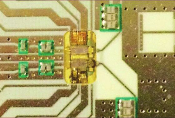
RF & Wireless
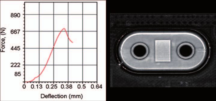
Figure 10: Thermal via array (left) vs. copper coin (right) Figure 11: a) Push-out force (left), b) sonic scan (right)
ped. The highest level of preci- condition at operating tempera- ture of printed circuit boards is a ded coins and embedded coins
sion can be achieved when the ture for example. The quality of proven and reliable technique. It can be used.
copper coins are inserted in a the bonding layer on adhesive provides a highly efficient way
sequential order, coin by coin. bonded copper coins is checked to dissipate heat from electronicThe principle of integrating
This process can be done fully in addition with ultra sonic scans components. coins into the PCB construc-
automated and the force that is (Figure 11b). tion is also suitable for bare die
provided during the coin inser- Various methods and techniques
The printed circuit boards have have been developed to provide attachment, providing a much
tion can be controlled and moni-
to pass several extensive reli- the circuit designer flexibility lower thermal resistance in the
tored for each individual coin.
ability and stress tests before in terms of board design and thermal pathway.
they are released for customer choice of materials. The advan-
How well the press-fitted copper applications. In some cases FEM tage over thermal via arrays has All of these techniques are esta-
coins are fastened in the PCB or simulations are supporting this been demonstrated. blished methods and are being
the bond strength of the adhesive phase of product development. already applied in a wide range
bonded copper coins is measured Table 2 lists some typical reli- The method of press-fitted of applications. They can be
by the so called push-out test, ability tests that printed circuit copper coins is the most attrac- found in automotive electronics,
a test that has been especially boards with copper coins must tive solution for the industry industrial electronics, and in tele-
developed for the copper coin pass. because the implementation is com infrastructure as well as in
technique (Figure 11a). This test very simple and does not require defence and avionics systems.
is typically done before and after Summary much effort, the costs are very Just recently press-fitted copper
some thermal stress. It also can reasonable. If larger coins are coins have been designed into
be performed with PCBs at some The integration of copper coins needed then some alternative the rigid section of rigid-flexible
elevated temperature to prove the for heat dissipation into the struc- methods such as adhesive bon- circuit board as well. ◄
Machine-to-Machine Applications with Industry Leading Cellular Engines
Skyworks Solutions, Inc. announced that switching. By supporting global and regi-
its SkyOne Ultra 2.5 and diversity receive onally optimized SKUs in the same PCB
(DRx) modules for mobile applications footprint, these platforms uniquely enable
have been adopted by some of the world’s cost-effective, high performance archi-
leading machine-to-machine (M2M) tectures with ultimate flexibility. Accor-
module manufacturers to provide high ding to a recent Cisco VNI report, M2M
performance, high speed 4G LTE capa- will be one of the fastest growing mobile
bility. These fully integrated and tested connection vehicles as global IoT appli-
systems, packaged in extremely small cations continue to gain traction in con-
form factors, enable M2M suppliers inclu- sumer and business environments. Cisco
ding Fibocom, Sierra Wireless, and Telit forecasts that globally, M2M connections
to extend plug and play, high-speed cel- will grow from 780 million in 2016 to 3.3
lular connectivity across an endless array
billion by 2021, at a compounded annual
of Internet of Things (IoT) products and
growth rate of 34 percent. Further, M2M
applications – in any global region and on
any wireless network. mobile connections will exceed a quarter
of total devices and connections by 2021,
SkyOne Ultra 2.5 covers over 20 LTE sitivity and cell edge performance while as devices evolve from 2G to 3G, 4G and
frequency bands in a complete front-end addressing all major downlink carrier higher technologies.
solution; inclusive of power amplification, aggregation combinations. This highly
duplex filtering and antenna switching. differentiated solution integrates low noise ■ Skyworks Solutions, Inc.
Skyworks’ DRx improves receiver sen- amplification, receive filtering, and band www.skyworksinc.com
78 hf-praxis 1/2018
You can also read