AVR2021: AT86RF231 Antenna Diversity

Page created by Doris Hoffman
 
CONTINUE READING
AVR2021: AT86RF231 Antenna Diversity

Features
• Self-contained Antenna Diversity algorithm
• Improves signal path robustness between nodes
• Direct register based antenna selection

1 Introduction                                                                           Application Note
Antenna Diversity is a transmission method using more than one antenna to
receive or transmit signals along different propagation paths to compensate for
multipath interferences.
Due to multipath propagation interference effects between network nodes, the
receive signal strength may strongly vary, even for small changes of the
propagation conditions, affecting the link quality. These fading effects can result in
an increased error floor or loss of the connection between devices.
Applying Antenna Diversity transmission techniques in such scenarios improves
the reliability of an RF connection between network nodes.
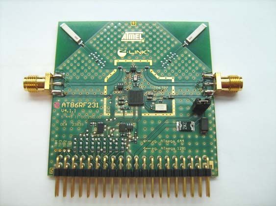
This application note describes the usage, design, and layout of the AT86RF231
Antenna Diversity, an implementation is shown in Figure 1-1. The information
provided is intended as a helping hand for hardware designers to make use of the
AT86RF231 Antenna Diversity capabilities.

        Figure 1-1. AT86RF231 – Antenna Diversity Radio Extender Board

                                                                                                Rev. 8158B-AVR-07/08
2 Wireless Communication Channel Models

2.1 Introduction
                    In wireless communication systems different channel models are used to describe the
                    behavior of the air interface. A simple model is additive white Gaussian noise
                    (AWGN). This model assumes a linear addition of wideband noise to the wanted
                    signal with a constant spectral density and a Gaussian distribution of the amplitude.
                    More realistic wireless channel models also consider the impact of multipath
                    propagation. Since a transmitted signal is subject to reflections and refraction on
                    walls, surfaces etc., the receiving node will see many signals, each differing in phase
                    and amplitude. All signals superpose at the receiving antenna causing an effect called
                    fading.
                    Using more than one antenna allows the evaluation of different multipath scenarios to
                    avoid or reduce the effects of fading or interferences. Assuming that these antennas
                    are independent of each other with respect to the signal propagation paths, the
                    probability that all of them suffer from fading at the same time is significantly reduced.

 2       AVR2021
                                                                                                8158B-AVR-07/08
AVR2021

3 AT86RF231 Antenna Diversity

3.1 Overview
                            The AT86RF231 Antenna Diversity (AD) feature supports the control of two antennas
                            to select the most reliable RF signal path.
                            A differential control pin pair, pin 9 (DIG1) and pin 10 (DIG2), is used to control an
                            external RF-switch selecting one of the two antennas. During synchronization header
                            (SHR) search, the radio transceiver autonomously switches between the two
                            antennas, without the need for microcontroller interaction, if the AD algorithm is
                            enabled.
                            To ensure highly uncorrelated receive signals on each antenna, the antennas should
                            be carefully separated from each other, refer to section 3.10.2.
                            If enabled, and when the AT86RF231 is set into a receive state, the automated AD
                            algorithm works as follows: On detection of an SHR with a sufficient high signal level
                            on one antenna, this antenna is locked for reception of PHR and PSDU. In this case,
                            no further attempt is made to determine the signal level on the other antenna.
                            Otherwise the SHR search is continued on the other antenna and vice versa.
                            After the completed reception of a frame, indicated by an interrupt IRQ_3
                            (TRX_END), the diversity search algorithm is continued until a new SHR header is
                            detected or the receive state is left.

3.2 Application Schematic
                            Figure 3-1 illustrates the AT86RF231 Application Schematic concentrating on
                            Antenna Diversity.

                            Figure 3-1. AT86RF231 Antenna Diversity – Application Schematic
                               ANT0
                                                              1   DIG3     AT86RF231
                                                              2 DIG4

                                         SW1       B1         3 AVSS

                                                              4 RFP
                                         Switch

                                                   Balun
                                          RF-

                                                              5 RFN
                                                                                DIG2
                                                                         DIG1

                                                              6 AVSS
                                                                  ...
                                                                         9      10

                               ANT1

                            Two antennas, ANT0 and ANT1, are connected via an RF-switch (SW1) to a
                            balun (B1). A differential control pin pair (DIG1/DIG2) selects one of the two signal
                            paths within SW1 to connect one antenna to the radio transceiver during receive or
                            transmit. Balun (B1) transforms the single-ended port impedance of 50Ω to the 100Ω
                            differential RF port impedance at pins RFP/RFN. For further details of the
                            AT86RF231 refer to [1].

                                                                                                                3
 8158B-AVR-07/08
3.3 Configuration
                                           It is recommended to configure Antenna Diversity in one of the transceiver states
                                           TRX_OFF, PLL_ON or TX_ARET_ON, for details refer to [1].
                                           Generally, the automated Antenna Diversity is enabled with register bit ANT_DIV_EN
                                           (register 0x0D, ANT_DIV) set. In addition, the control of the Antenna Diversity
                                           RF-switch (SW1) must be enabled by register bit ANT_EXT_SW_EN (register 0x0D,
                                           ANT_DIV). In this case the internal pull-down of the control pins DIG1/DIG2 is
                                           disabled, and they feed the antenna switch signal and its inverse to the differential
                                           control inputs of SW1. The voltage level of DIG1/DIG2 is equal to DEVDD.
                                           To actually receive a frame, applying the AD algorithm, the AT86RF231 state must be
                                           changed to RX_ON or RX_AACK_ON.

3.4 Receive Diversity Procedure
                                           Exemplary, the function and behavior of the control signals DIG1/DIG2 during receive
                                           is shown in Figure 3-2.

Figure 3-2. Antenna Diversity Operating Principle during Receive
                                     0     64                                                   512                                                                  time [µs]

            Frame on ANT0                                                                                                             SHR         PHR          PSDU
On
Air

            Frame on ANT1                  SHR         PHR              PSDU (ACK=0)

            TRX_STATE              RX_ON                                    BUSY_RX                                      RX_ON                                BUSY_RX
Control
 TRX

            IRQ                                                  RX_START                 AMI         TRX_END                                             RX_START

            Antenna selection   Search                           RX Antenna Selected                                        Search                RX Antenna Selected
Diversity
Antenna

            DIG1
                                                 ANT1 selected                                                                                ANT0 selected
            DIG2

                                 41 µs
            ANT_SEL                                               ANT1 selection stored                                                                 ANT0 selection stored

                                                (1)       (2)                                   (3)                                         (1)     (4)

                                           Assuming a frame with a sufficient signal level is available at antenna ANT1 only, the
                                           AD algorithm selects this antenna while searching for the SHR (1). During the rest of
                                           the frame reception this configuration is fixed. The selected antenna can be
                                           determined by reading register bit ANT_SEL at the time when interrupt IRQ_2
                                           (RX_START) is issued (2).
                                           Immediately after the successful frame reception, indicated by an interrupt IRQ_3
                                           (TRX_END), the AD algorithm starts searching again (3). This continues as long as
                                           the radio transceiver is in RX_ON or RX_AACK_ON state. Leaving one of the receive
                                           states stops the AD algorithm.
                                           The register bit ANT_SEL maintains its previous value (from the last received frame)
                                           until a new frame has been detected, indicated by IRQ_2 (RX_START), see (4). That
                                           is at the earliest:
                                                        tTR,ANT_SEL = tTR27 + 2 · tsym,                         for tTR27 = 96 µs, tsym = 16 µs, refer to [1]
   4               AVR2021
                                                                                                                                                           8158B-AVR-07/08
AVR2021
                         If the AT86RF231 is not in a receive state or a transmit state, it is recommended to
                         disable register bit ANT_EXT_SW_EN to reduce the power consumption or avoid
                         leakage current of an external RF-switch, especially during SLEEP state. If register bit
                         ANT_EXT_SW_EN = 0, output pins DIG1/DIG2 are pulled-down.

3.5 Transmit Diversity Procedure
                         With the AT86RF231 Antenna Diversity feature, upon reception of a frame, the
                         selected antenna is indicated by register bit ANT_SEL. This register bit maintains its
                         value until a following frame has been detected, refer to 3.4.
                         In contrast to that, the antenna defined by register bits ANT_CTRL (register 0x0D,
                         ANT_DIV) is used for transmission. If, for example, the same antenna should be used
                         for transmission as being selected by the AT86RF231 for reception, the antenna must
                         be set using register bits ANT_CTRL (register 0x0D, ANT_DIV), according to the
                         value read from register bit ANT_SEL. At the earliest, IRQ_2 (RX_START), as an
                         indication of successful PHR reception, can be used to set register bits ANT_CTRL,
                         refer to Figure 3-3 (1). However, for RX_AACK it is recommended to enable IRQ_3
                         (TRX_END) only, refer to [1]. This interrupt is issued if a frame passes the frame
                         filtering and has a valid FCS.
                         When reading register bit ANT_SEL, e.g. after IRQ_3 (2), the timing requirements of
                         the succeeding operation have to be taken into account:
                             1. Transmitting an acknowledgement frame requires setting of the transmit
                                antenna after occurrence of IRQ_3 within aTurnaroundTime [3]:
                                         tTR,ANT_CTRL = 12 · tsym
                             2. Transmitting an acknowledgement frame in slotted operation mode requires
                                setting of the transmit antenna after occurrence of IRQ_3:
                                         tTR,ANT_CTRL = 6 · tsym

                         As an example, the application of Antenna Diversity in Extended Operating Mode
                         RX_AACK is shown in Figure 3-3. In contrast to the example in Figure 3-2, an
                         acknowledgement frame is automatically transmitted after aTurnaroundTime (3). To
                         define, that the same antenna is used for transmission as for reception, the register
                         bits ANT_CTRL are to be set within tTR,ANT_CTRL, accordingly, see above.

                                                                                                               5
 8158B-AVR-07/08
Figure 3-3. Antenna Diversity in Extended Operating Mode
                                              0     64                                                  512                      704                          1088      time [µs]

                     Frame on ANT0
On
Air

                     Frame on ANT1                   SHR         PHR            PSDU (ACK=1)                                                     ACK Frame

                     TRX_STATE           RX_AACK_ON                                                           BUSY_RX_AACK                                         RX_AACK_ON
Control
 TRX

                     RX/TX                                       RX                                                                                 TX                 RX

                     IRQ                                                 RX_START                 AMI         TRX_END

                     Antenna selection   Search                          RX Antenna Selected                                   TX antenna set by ANT_CTRL            Search
 Antenna Diversity

                     DIG1
                                                         ANT1 selected
                     DIG2

                     ANT_SEL                                              ANT1 selection stored                 tTR,ANT_CTRL

                     ANT_CTRL              0x02 (ANT0)                                                        Set ANT_CTRL                    0x01 (ANT1)

                                                                   (1)                                  (2)                      (3)                         (4)

                                                    In general, the AD algorithm and timings are identical for Basic and Extended
                                                    Operating Modes, refer to [1].

3.6 Dynamic and Static Antenna Selection
                                                    Even without using the automated AD algorithm, one antenna can be selected
                                                    permanently. This may be useful if the Antenna Diversity selection is performed using
                                                    another control entity than the PHY.
                                                    To select one antenna permanently, the antenna has to be configured using register
                                                    bits ANT_CTRL. This setting defines the antenna for a transmission as well as for
                                                    reception. The AD algorithm shall be disabled (register bit ANT_DIV_EN = 0) and the
                                                    control of RF-switch shall be enabled (register bit ANT_EXT_SW_EN = 1).

3.7 Antenna Diversity Sensitivity Control
                                                    Due to a different receive algorithm used by the AD algorithm, the sensitivity of the
                                                    receiver has to be adjusted. To achieve this it is recommended to set register bits
                                                    PDT_THRES (register 0x0A, RX_CTRL) to 0x3.
                                                    If the AD algorithm control is disabled, and one antenna is permanently selected
                                                    using register bits ANT_CTRL, the register bits PDT_THRES shall be reset.

   6                         AVR2021
                                                                                                                                                               8158B-AVR-07/08
AVR2021
3.8 Register Description
                           Register 0x0A (RX_CTRL):
                           The RX_CTRL controls the sensitivity of the Antenna Diversity Mode.
                           Bit                 7                6                5                 4
                           0x0A             Reserved      Reserved           Reserved          Reserved         RX_CTRL
                           Read/Write         R/W              R/W              R/W              R/W
                           Reset Value         1                0                1                1

                           Bit                 3                2                1                 0
                           0x0A          PDT_THRES       PDT_THRES         PDT_THRES         PDT_THRES          RX_CTRL
                           Read/Write         R/W              R/W              R/W              R/W
                           Reset Value         0                1                1                1

                           • Bit 7:4 – Reserved

                           • Bit 3:0 – PDT_THRES
                           These register bits control the sensitivity of the receiver correlation unit. If the
                           AD algorithm is enabled, the value shall be set to PDT_THRES = 3, otherwise it shall
                           be set back to the reset value.
                           Table 3-1. Receiver Sensitivity Control
                             Register Bit              Value         Description
                             PDT_THRES                  0x7          Reset value, to be used if AD algorithm is disabled
                                                        0x3          Recommended correlator threshold if AD algorithm
                                                                     is enabled
                                                       Other         Reserved

                           Register 0x0D (ANT_DIV):
                           The ANT_DIV register configures and controls Antenna Diversity.
                           Bit                 7                6                  5               4
                           0x0D             ANT_SEL       Reserved            Reserved         Reserved         ANT_DIV
                           Read/Write         R                R                   R               R
                           Reset Value        0                0                   0               0

                           Bit                 3                2                  1               0
                           0x0D          ANT_DIV_EN    ANT_EXT_SW_EN         ANT_CTRL          ANT_CTRL         ANT_DIV
                           Read/Write        R/W               R/W              R/W               R/W
                           Reset Value        0                 0                1                 1

                           • Bit 7 – ANT_SEL
                           This register bit signals the currently selected antenna path. The selection is based
                           either on the last antenna diversity cycle, if automated Antenna Diversity is enabled
                           (ANT_DIV_EN = 1), or on the content of register bits ANT_CTRL, for details refer to
                           3.5.

                                                                                                                           7
 8158B-AVR-07/08
Table 3-2. Antenna Diversity - Antenna Selection
               Register Bit                Value       Description
               ANT_SEL                       0         Antenna 0
                                             1         Antenna 1

              • Bit 6:4 – Reserved

              • Bit 3 – ANT_DIV_EN
              This register bit controls the AD algorithm. On reception of a frame the algorithm
              selects an antenna autonomously during SHR search. This selection is kept until:
              • A new SHR search starts
              • The receive state is left
              • Disabling AD algorithm
                          o Selected antenna is defined by register bits ANT_CTRL

              Table 3-3. Antenna Diversity Algorithm Control
               Register Bit                Value       Description
               ANT_DIV_EN                    0         Automated AD algorithm disabled
                                             1         Automated AD algorithm enabled
               Note:    If ANT_DIV_EN = 1 register bit ANT_EXT_SW_EN shall be set to 1, too.

              • Bit 2 – ANT_EXT_SW_EN
              If enabled, pin 9 (DIG1) and pin 10 (DIG2) become output pins and provide a
              differential control signal for an Antenna Diversity switch. The selection of a specific
              antenna is done either by the AD algorithm (ANT_DIV_EN = 1), or according to
              register bits ANT_CTRL if the AD algorithm is disabled.
              Do not enable Antenna Diversity RF-switch control (ANT_EXT_SW_EN = 1) and RX
              Frame Time Stamping (IRQ_2_EXT_EN = 1) at the same time, refer to [1].
              As long as register bit ANT_EXT_SW_EN is set, the control pins DIG1/DIG2 are
              activated in all radio transceiver states. If the AT86RF231 is not in a receive or
              transmit state, it is recommended to disable register bit ANT_EXT_SW_EN to reduce
              the power consumption or avoid leakage current of an external RF-switch, especially
              during SLEEP state. If register bit ANT_EXT_SW_EN = 0, output pins DIG1 and
              DIG2 are pulled-down.
              Table 3-4. Antenna Diversity RF-Switch Control
               Register Bit                Value       Description
               ANT_EXT_SW_EN                 0         Antenna Diversity RF-switch control disabled
                                             1         Antenna Diversity RF-switch control enabled
               Notes:         1.   If ANT_DIV_EN = 1 register bit ANT_EXT_SW_EN shall be set to 1, too.
                              2.   If ANT_EXT_SW_EN = 1 register bit IRQ_2_EXT_EN shall be set to 0.

8   AVR2021
                                                                                             8158B-AVR-07/08
AVR2021
                  • Bit 1:0 – ANT_CTRL
                  These register bits provide a direct, static control of an Antenna Diversity switch.
                  Setting ANT_DIV_EN = 0 (Antenna Diversity disabled), this register setting defines
                  the transmit or receive antenna.
                  Table 3-5. Antenna Diversity - Static Antenna Selection
                   Register Bit            Value       Description
                   ANT_CTRL                  0         Reserved
                                             1         Antenna 1,        DIG1 = H
                                                                         DIG2 = L
                                             2         Antenna 0,        DIG1 = L
                                                                         DIG2 = H
                                             3         Default value for ANT_EXT_SW_EN = 0.
                                                       Mandatory setting for applications not using AD.
                   Note:   The register values 1     and   2   are   mandatory   for   ANT_DIV_EN=1       and
                           ANT_EXT_SW_EN = 1.

                                                                                                          9
8158B-AVR-07/08
3.9 AT86RF231 Antenna Diversity - Radio Extender Board

3.9.1 Overview
                        An AT86RF231 Radio Extender Board supporting Antenna Diversity (AD-REB) is
                        shown in Figure 1-1. The interface between the radio transceiver and the
                        microcontroller is similar to the basic application schematic as shown in [1].

3.9.2 Schematic
                        An excerpt of the AD-REB schematic with focus on the RF section is shown in Figure
                        3-4.

                        Figure 3-4. AT86RF231 AD-REB RF Section Schematic
                                 ANT0                                   50Ohm                                                        50Ohm                                          ANT1
                                 2.45 GHz                                      i                                                          i                                         2.45 GHz
                                                                                      3

                                                                                                   2

                                                                                                                1
                                                                                                                       U3
                                                                                                                       AS222-92
                                                                                          J2

                                                                                                                J3
                                                                                                   GND
                                                                               V1 = !V2

                                                                                                                  H
                                                                                            H
                                                                                          V1

                                                                                                                V2
                                                                                                   J1
                                                                                      4

                                                                                                   5

                                                                                                                6

                                       R1                                                                                                                                   R2
                          DIG1                                                                                                                                                      DIG2
                                        2k2                                                                     i 50Ohm                                                       2k2
                                              C3                                                                                                                     C4
                                              22pF                                                                                                                   22pF
                                                                                      2

                                                                                                   1

                                                                                                                5
                                                                                                   unbalanced

                                                                                                                                                6
                                                                                                                GND
                                                                                          DC_GND

                                                                                                                                     nc
                                                                        Balanced P1

                                                                                                                       Balanced P2

                                                                                                                                                U2
                                                                                                                                                Balun
                                                                    3

                                                                                                                      4

                                                                                      C1                                             C2
                                                                                      22pF                                           22pF
                         DIG2
                                DIG1

                                                                                           RFN
                                                                                                      RFP

                                                                                                                                                                  U1
                                                            8

                                                                   7

                                                                            6

                                                                                            5

                                                                                                       4

                                                                                                                  3

                                                                                                                           2

                                                                                                                                          1

                                                                                                                                                                  AT86RF231
                                                                                                           RFP
                                                                                               RFN
                                                            RSTN

                                                                   DVSS

                                                                                   AVSS

                                                                                                                    AVSS

                                                                                                                                DIG4

                                                                                                                                              DIG3

                                                 9                                                                                                           32
                                                     DIG1                                                                                             AVSS
                                                10                                                                                                           31
                                                     DIG2                                                                                             AVSS
                                                11                                                                                                           30
                                                     SLP_TR                                                                                           AVSS
                                                12                                    AT86RF231                                                              29
                                                     DVSS                                                                                            AVDD
                                                13                                            MLF32                                                          28
                                                     DVDD                                                                                            EVDD
                                                14                                                                                                           27
                                                     DVDD                                                                                             AVSS
                                                15                                                                                                           26
                                                     DEVDD                                                                                           XTAL1
                                                16                                                                                                           25
                                                     DVSS                                                                                            XTAL2
                                                            CLKM

                                                                                   SCLK
                                                                   DVSS

                                                                                                           DVSS
                                                                                               MISO

                                                                                                                    MOSI

                                                                                                                                SEL

                                                                                                                                              IRQ

                                                                                                                                                             33
                                                                                                                                                       DIE
                                                            17

                                                                   18

                                                                            19

                                                                                            20

                                                                                                       21

                                                                                                                  22

                                                                                                                           23

                                                                                                                                          24

 10        AVR2021
                                                                                                                                                                                               8158B-AVR-07/08
AVR2021
3.9.3 Layout

                              Figure 3-5. AT86RF231 AD-REB RF Section Layout

3.9.4 Diversity Antenna Considerations and Implementation Details
                              The AT86RF231 AD-REB implementation makes use of both, space and polarization
                              diversity. Polarization diversity is the ability to receive orthogonally polarized waves
                              with independent propagation characteristics. Therefore the antennas are placed with
                              a specific distance and angle. The distance can be derived, for instance, from the
                              width of the deep fade regions as shown in Figure 3-8.

                              Figure 3-6. Antenna Configuration Examples

                              The placement onto the PCB FR4-substrate plane offers various possibilities in the
                              configuration of the two antennas, as shown in Figure 3-6. The first and the second
                              example using different polarization planes. Here the antennas are placed with an
                              angle of 90 degrees to each other. The advantage of the second configuration is a
                              higher symmetry, which makes antenna matching and board layout easier. The third
                              antenna placement is a symmetric configuration, however, does not support
                              polarization diversity.
                              Additional Notes:
                              • The RC components placed between pins DIG9/10 and the RF-switch filter
                                possible transient switching noise of the AT86RF231 control pins, to avoid
                                coupling into the antenna paths. The RC filter consists of R1-C3 / R2-C4.
                              • RF-switch (SW1) is recommended to have low insertion loss (typ. < 1 dB) and high
                                isolation (typ. > 20 dB). No DC path should exist in the antenna paths to make
                                switching with single ended positive voltages possible, refer to the RF-switch
                                datasheet.
                              • The antenna paths are grounded coplanar lines with a characteristic impedance of
                                50 Ohm.
                              • The SW1 switching time to select one antenna should be below 1 µs.

                                                                                                                   11
 8158B-AVR-07/08
3.9.5 Bill of Material
                         Table 3-6. AT86RF231 AD-REB – RF Section Bill-of-Material (BoM)
                          Designator                Value    Description
                          ANT0, ANT1          2.45 GHz       Ceramic antennas
                          C1, C2, C3, C4      22pF           Ceramic capacitor
                          R1, R2              2k2            Resistor
                          U1                  AT86RF231      802.15.4 2.4GHz Radio Transceiver, refer to [1]
                          U2                  WE748421245    SMD-BALUN, Würth
                          U3                  AS222-92       RF-Switch, Skyworks

 12          AVR2021
                                                                                                  8158B-AVR-07/08
AVR2021
3.10 Measurement Results

3.10.1 Measurement Setup
                           Measurements are provided to demonstrate the performance improvement of a
                           network node operating in a typical multipath indoor environment when using Antenna
                           Diversity compared to a predefined antenna configuration.

                           Figure 3-7. Antenna Diversity Measurement Setup
                                                                                                        AD-Receiver
                                                                                            RX
                                                                                                        - moveable

                                                                    1400 mm

                                                                                                 Metal plate
                                                                                                 - remove direct line-of-sight

                                                                                                 Transmitter
                                                                       TX
                                                                                                 - fixed position

                           Node 1 (RX), equipped with two antennas, see Figure 1-1, is stepwise moved along a
                           fixed track. Node 1 stops at each measurement point. It receives a frame and
                           evaluates its energy detection (ED) level, refer to [1].
                           Node 2 (TX) is situated in a fixed position, permanently transmitting frames. The
                           transmitter is equipped with only one 2.4 GHz λ/4 whip antenna and therefore does
                           not use transmit Antenna Diversity.
                           The measurement setup has no direct line-of-sight between the two nodes. Therefore
                           the propagation scenario is determined by multipath. Additionally, the scenario of the
                           indoor environment must be kept static during the measurement process.
                           To investigate the multipath propagation characteristics, see Figure 3-8, the transmit
                           power is set such that the average receiving power is between -60 to -65 dBm.
                           During the PER measurements, the transmit power of node 2 is adjusted (see Figure
                           3-9) to reduce the average received signal power to a value slightly above the
                           sensitivity limit of -101 dBm, refer to [1]. This is necessary to illustrate the effect of
                           deep fades and to create a reasonable average packet error rate.
                           At each track position the packet error rate (PER) is measured, using 200 packets
                           and a frame length of 50 octets.

                                                                                                                          13
 8158B-AVR-07/08
3.10.2 Multipath Propagation Characteristics
                               Exemplary, a measurement result of a 2.4 GHz multipath scenario in a laboratory
                               environment is shown in Figure 3-8. One curve represents the received signal power
                               at one single antenna. The received signal power is measured at each antenna
                               separately using an ED measurement.

                               Figure 3-8. Multipath Propagation Fading Effects
                                                  -40

                                                  -45                                                 left antenna
                                                                                                      right antenna
                                                  -50

                                                  -55
                                 ED Level [dBm]

                                                  -60

                                                  -65

                                                  -70

                                                  -75

                                                  -80
                                                                        deep fades

                                                  -85

                                                  -90
                                                        0   200   400      600           800   1000     1200           1400
                                                                             position [mm]

                               The received signal power at the two antennas varies up to more than 25 dB at
                               certain measurement points, refer to positions 380 mm and 850 mm for instance, or
                               up to 35 dB over the measurement distance. When assuming a larger distance
                               between the two nodes or a more complicate multipath scenario the average received
                               signal power is significant lower. Then one antenna may not receive a sufficient high
                               signal power to correctly receive a frame. In this case the other antenna is selected to
                               receive the frame.
                               Figure 3-8 further shows that a distance of about λ/2 between the two diversity
                               antennas is required to effectively distinguish between different multipath channels.
                               The AT86RF231 Antenna Diversity Radio Extender Board V-shape placement of the
                               two antennas offers in addition linear antenna polarization. This improves the ability to
                               separate between orthogonally polarized multipath channels.
                               Even if in this example node 1 changes its position, a similar behavior is observed if
                               the environment changes and the two nodes are at a fixed position.

 14        AVR2021
                                                                                                               8158B-AVR-07/08
AVR2021
3.10.3 Network Performance Measurements
                                          A measurement illustrating the node-to-node performance using the packet error rate
                                          (PER) is shown in Figure 3-9. The result consists of three individual measurements:
                                          1. Use ANT0 only                   (left antenna)
                                          2. Use ANT1 only                   (right antenna)
                                          3. AD algorithm enabled            (auto decision)

                                          When using Antenna Diversity there are three possible scenarios for two antennas:
                                          1. Both antennas behave different:
                                                      o One antenna with a good signal quality            (PER Æ 0)
                                                      o The other does not receive                        (PER Æ 1)
                                          2. Both antennas provide a good signal quality                  (PER Æ 0)
                                          3. Both antennas do not receive                                 (PER Æ 1)

Figure 3-9. Antenna Diversity Validation Results
         1

                                             (3 )
        0,9
                                                                             A NT0
        0,8                                                                  A uto De cisi on
                                                                             A NT1
        0,7

        0,6
  PER

        0,5

        0,4

        0,3                                                   (1 )

        0,2
                                                                                                        (1)
        0,1       (1)        (1)
                                                                                    (2)
         0
              0         50         1 00     1 50       2 00          25 0    30 0          350   4 00         4 50     5 00
                                                        track position [mm ]

                                              Re ce iv er still do es re ceive

                                          The measurement result in Figure 3-9 shows that for scenarios of type (1), when one
                                          antenna is receiving while the other one doesn’t, the resulting PER is still at an
                                          acceptable low level when using the AD algorithm.
                                          If both antennas provide a sufficient high signal quality (scenario 2) the Antenna
                                          Diversity can not improve the link quality further.
                                          Only if both antennas do not receive anything, also Antenna Diversity can’t provide
                                          better results, scenario type (3).

                                                                                                                              15
 8158B-AVR-07/08
4 Conclusion
                 In environments with distinctive multipath scenarios or varying propagation conditions
                 the application of Antenna Diversity ensures a significant higher probability to access
                 a network node. Thus connectivity between network nodes is improved.
                 Effects, that nodes are not accessible since they are in a deep fade, are prevented.
                 This may happen even in well established network installation, if for examples the
                 environmental conditions changes.
                 The use of the AT86RF231 Antenna Diversity transmission technique considerably
                 improves the reliability of real-world network implementations.
                 This is achieved without increasing the link budget of a network connection, e.g. by
                 using a higher transmit power or and additional pre-amplification (LNA) during
                 receive.

 16    AVR2021
                                                                                          8158B-AVR-07/08
AVR2021

5 Abbreviations
                   AD     -   Antenna Diversity
                   AWGN   -   Additive White Gaussian Noise
                   ED     -   Energy Detection
                   PER    -   Packet Error Rate
                   PHR    -   PHY Header
                   PHY    -   Physical Layer
                   PSDU   -   PHY Service Data Unit
                   REB    -   Radio Extender Board
                   RX     -   Receiver
                   SHR    -   Synchronization Header
                   SWPM   -   Software Programming Model
                   TX     -   Transmitter

                                                                    17
 8158B-AVR-07/08
6 References
                 [1]   AT86RF231; Low Power, 2.4 GHz Transceiver for ZigBee, IEEE 802.15.4, and
                       ISM Applications; Datasheet; Rev. 8111A-AVR-04/08; Atmel Corporation
                 [2]   AT86RF231; Software Programming Model; Rev.1.1; Atmel Corporation
                 [3]   IEEE Std 802.15.4™: Wireless Medium Access Control (MAC) and Physical
                       Layer (PHY) Specifications for Low-Rate Wireless Personal Area Networks (LR-
                       WPANs)

 18    AVR2021
                                                                                     8158B-AVR-07/08
AVR2021

7 EVALUATION BOARD/KIT IMPORTANT NOTICE
                   This evaluation board/kit is intended for use for FURTHER ENGINEERING,
                   DEVELOPMENT, DEMONSTRATION, OR EVALUATION PURPOSES ONLY. It is
                   not a finished product and may not (yet) comply with some or any technical or legal
                   requirements that are applicable to finished products, including, without limitation,
                   directives regarding electromagnetic compatibility, recycling (WEEE), FCC, CE or UL
                   (except as may be otherwise noted on the board/kit). Atmel supplied this board/kit
                   “AS IS,” without any warranties, with all faults, at the buyer’s and further users’ sole
                   risk. The user assumes all responsibility and liability for proper and safe handling of
                   the goods. Further, the user indemnifies Atmel from all claims arising from the
                   handling or use of the goods. Due to the open construction of the product, it is the
                   user’s responsibility to take any and all appropriate precautions with regard to
                   electrostatic discharge and any other technical or legal concerns.
                   EXCEPT TO THE EXTENT OF THE INDEMNITY SET FORTH ABOVE, NEITHER
                   USER NOR ATMEL SHALL BE LIABLE TO EACH OTHER FOR ANY INDIRECT,
                   SPECIAL, INCIDENTAL, OR CONSEQUENTIAL DAMAGES.
                   No license is granted under any patent right or other intellectual property right of
                   Atmel covering or relating to any machine, process, or combination in which such
                   Atmel products or services might be or are used.
                   Mailing Address: Atmel Corporation, 2325 Orchard Parkway, San Jose, CA 95131
                   Copyright © 2008, Atmel Corporation

                                                                                                        19
 8158B-AVR-07/08
Disclaimer
 Headquarters                          International
 Atmel Corporation                     Atmel Asia                           Atmel Europe                          Atmel Japan
 2325 Orchard Parkway                  Room 1219                            Le Krebs                              9F, Tonetsu Shinkawa Bldg.
 San Jose, CA 95131                    Chinachem Golden Plaza               8, Rue Jean-Pierre Timbaud            1-24-8 Shinkawa
 USA                                   77 Mody Road Tsimshatsui             BP 309                                Chuo-ku, Tokyo 104-0033
 Tel: 1(408) 441-0311                  East Kowloon                         78054 Saint-Quentin-en-               Japan
 Fax: 1(408) 487-2600                  Hong Kong                            Yvelines Cedex                        Tel: (81) 3-3523-3551
                                       Tel: (852) 2721-9778                 France                                Fax: (81) 3-3523-7581
                                       Fax: (852) 2722-1369                 Tel: (33) 1-30-60-70-00
                                                                            Fax: (33) 1-30-60-71-11

                                       Product Contact

                                       Web Site                             Technical Support                     Sales Contact
                                       www.atmel.com                        avr@atmel.com                         www.atmel.com/contacts

                                       Literature Request
                                       www.atmel.com/literature

 Disclaimer: The information in this document is provided in connection with Atmel products. No license, express or implied, by estoppel or otherwise, to any
 intellectual property right is granted by this document or in connection with the sale of Atmel products. EXCEPT AS SET FORTH IN ATMEL’S TERMS AND
 CONDITIONS OF SALE LOCATED ON ATMEL’S WEB SITE, ATMEL ASSUMES NO LIABILITY WHATSOEVER AND DISCLAIMS ANY EXPRESS, IMPLIED
 OR STATUTORY WARRANTY RELATING TO ITS PRODUCTS INCLUDING, BUT NOT LIMITED TO, THE IMPLIED WARRANTY OF MERCHANTABILITY,
 FITNESS FOR A PARTICULAR PURPOSE, OR NON-INFRINGEMENT. IN NO EVENT SHALL ATMEL BE LIABLE FOR ANY DIRECT, INDIRECT,
 CONSEQUENTIAL, PUNITIVE, SPECIAL OR INCIDENTAL DAMAGES (INCLUDING, WITHOUT LIMITATION, DAMAGES FOR LOSS OF PROFITS,
 BUSINESS INTERRUPTION, OR LOSS OF INFORMATION) ARISING OUT OF THE USE OR INABILITY TO USE THIS DOCUMENT, EVEN IF ATMEL HAS
 BEEN ADVISED OF THE POSSIBILITY OF SUCH DAMAGES. Atmel makes no representations or warranties with respect to the accuracy or completeness of the
 contents of this document and reserves the right to make changes to specifications and product descriptions at any time without notice. Atmel does not make any
 commitment to update the information contained herein. Unless specifically provided otherwise, Atmel products are not suitable for, and shall not be used in,
 automotive applications. Atmel’s products are not intended, authorized, or warranted for use as components in applications intended to support or sustain life.

 © 2008 Atmel Corporation. All rights reserved. Atmel®, logo and combinations thereof, AVR®, Z-Link® logo and others, are the registered
 trademarks, or trademarks of Atmel Corporation or its subsidiaries. Other terms and product names may be trademarks of others.

                                                                                                                                              8158B-AVR-07/08
You can also read