Microlens arrays with adjustable aspect ratio fabricated by electrowetting and their application to correlated color temperature tunable ...
←
→
Page content transcription
If your browser does not render page correctly, please read the page content below
Vol. 27, No. 4 | 18 Feb 2019 | OPTICS EXPRESS A25

Microlens arrays with adjustable aspect ratio
fabricated by electrowetting and their
application to correlated color temperature
tunable light-emitting diodes
JUNCHI CHEN,1,4 BENJAMIN FRITZ,2,4 GUANWEI LIANG,1 XINRUI DING,1,*
ULI LEMMER,2,3 AND GUILLAUME GOMARD2,3,5
1
  South China University of Technology, China
2
  Light Technology Institute (LTI), Karlsruhe Institute of Technology (KIT), Engesserstrasse 13, 76131
Karlsruhe, Germany
3
  Institute of Microstructure Technology (IMT), Karlsruhe Institute of Technology (KIT), Hermann-von-
Helmholtz-Platz 1, 76344 Eggenstein-Leopoldshafen, Germany
4
  These authors contributed equally
5
  guillaume.gomard@kit.edu
*
  dingxr@scut.edu.cn

Abstract: We develop a facile, fast, and cost-effective method based on the electrowetting
effect to fabricate concave microlens arrays (MLA) with a tunable height-to-radius ratio,
namely aspect ratio (AR). The electric parameters including voltage and frequency are
demonstrated to play an important role in the MLA forming process. With the optimized
frequency of 5 Hz, the AR of MLA are tuned from 0.057 to 0.693 for an increasing voltage
from 0 V to 180 V. The optical properties of the MLA, including their transmittance and light
diffusion capability, are investigated by spectroscopic measurements and ray-tracing
simulations. We show that the overall transmittance can be maintained above around 90%
over the whole visible range, and that an AR exceeding 0.366 is required to sufficiently
broaden the transmitted light angular distribution. These properties enable to apply the
developed MLA films to correlated-color-temperature (CCT)-tunable light-emitting-diodes
(LEDs) to enhance their angular color uniformity (ACU). Our results show that the ACU of
CCT-tunable LEDs is significantly improved while preserving almost the same lumen output,
and that the MLA with the highest AR exhibits the best ACU performance.

© 2019 Optical Society of America under the terms of the OSA Open Access Publishing Agreement

1. Introduction
Microlens arrays (MLA) are micro-optical elements widely used in optical sensors [1],
photovoltaics [2], 3D displays [3] as well as for light management in light emitting diodes
(LEDs) [4,5]. The LED technology offers unique advantages compared to traditional
incandescent bulbs and fluorescent lamps including a high efficiency, a low power
consumption and a long lifetime [6–9]. To meet the demands of high-quality illumination and
display, the angular color uniformity (ACU) of LEDs needs further improvement [10–12].
Numerous methods have been proposed to ameliorate the ACU of white LEDs, such as light
scattering nano-particles [13,14], shaped phosphor layers [15,16], diffusing reflectors [17]
and microstructured films [18,19]. Among these different approaches, the microstructured
films method is particularly attractive as it is facile and suitable for various LED packages,
and has been widely adopted in commercial applications. Furthermore, Chen et al.
demonstrated that diffusing MLA significantly improve the ACU of correlated color
temperature (CCT)-tunable LEDs [20], which motivated the present work. As a new type of
intelligent LED light source, a CCT-tunable LED changes the CCT by independently
adjusting the light intensity of cold and warm color light [21,22]. Because of the lack of a

#347980                                                                 https://doi.org/10.1364/OE.27.000A25
Journal © 2019           Received 12 Oct 2018; revised 7 Dec 2018; accepted 7 Dec 2018; published 17 Jan 2019
Vol. 27, No. 4 | 18 Feb 2019 | OPTICS EXPRESS A26

proper light mixing scheme, CCT-tunable LED lamps suffer from a poor color uniformity and
from the appearance of a blue circle and a yellow halo, which are detrimental to the
illumination quality [23]. In our previous research, we effectively improved the ACU of
CCT-tunable LEDs by MLA, reducing the CCT deviation from 1090 K to 218 K within the
CCT range of 3000-4000 K [20]. Herein, the MLA morphology and more specifically their
aspect ratio (AR), defined as the ratio of their height over their base radius, is a key factor for
the ACU performance, which still needs to be investigated.
    The increasing demand for micro-optoelectronic devices has prompted the development of
MLA fabrication methods including direct laser writing [24–26], reactive ion etching [27,28],
cylindrical micropillars photoresist reflow [29–31], hot embossing [32–34] and inkjet printing
[35,36]. Direct laser writing enables fabrication of MLA with different shapes. However, it is
not suitable for mass fabrication because it is a serial process. Reactive ion etching requires
vacuum which is slowing down fabrication. Photoresist reflow and hot embossing methods
have the advantages of low cost and high surface flatness, but the lens morphology is hard to
control. Many studies have shown that the microlenses shape has a significant impact on the
MLA performance [37–39], hence the fabrication of morphology-controllable MLA has
attracted much attention. Xu et al. controlled the curvature of the acrylate resin concave
meniscus in a patterned PDMS template. To this end, the interfacial energy was adjusted by
the processing time for the surface modification of the PDMS microholes [40]. Fang et al.
used the UV laser writing method coupled with soft imprint technology to fabricate
paraboloidal MLA with varying ARs, which can be easily tuned by changing the exposure
laser power [41]. A breath figure method based on water fog condensing was proposed by
Peng et al. to fabricate the MLA by adjusting the condensing temperature and time [42]. Yang
et al. proposed to fabrication hexagonal compound eye MLA using a maskless lithography
technique based on digital micromirror device which allowed a proper control of the
morphology. To achieve this, three steps were involved and a final reflow process was
required to smoothen the lenses' surface [43]. The above described methods can form MLA
structures with varying ARs, but they do not allow to rapidly change them during fabrication.
    In our study, we propose to exploit a versatile, potentially low-cost and rapid route based
on the electrowetting effect in order to fabricate concave MLA with controllable lens
curvature [44,45]. The electrowetting phenomenon refers to the change in solid-liquid contact
angle due to an applied potential difference between the solid and the liquid [46]. In our
approach, liquid UV-cured polymer is filling the micro-holes of a patterned silicon template,
whose preparation only requires one initial wet etching step and determines the diameter and
arrangement of the MLA. Their AR can then be controlled by adjusting the voltage and
frequency between the silicon template and the polymer which changes the contact angle of
the polymer surface. In this contribution, we specifically tune these electrical parameters with
a view to maximizing the AR of the MLA. Our objective is here to broaden the transmitted
light angular distribution, to promote light mixing and in turn, to improve the ACU of CCT-
tunable LED lamps. This demonstration is supported in the next sections by both
spectroscopic measurements and (ray tracing) optical simulations, and by testing the
developed MLA in CCT-tunable LED lamps.
2. Experimental and simulation methods
2.1 Fabrication of MLA with tunable AR by electrowetting
The concave MLA fabrication method we use requires a micro-patterned template and the
application of an electrical field, as schematized in Fig. 1. First, UV curable polymer
(Norland optical adhesive 65) was spin-coated on a glass substrate covered by a transparent
conductive indium tin oxide (ITO) layer (Shenzhen Xiangcheng). A P-type doped conductive
silicon template (with electrical resistance between 1 and 10Ω/cm), drilled by a hexagonal
array of cylindrical micro-holes, was placed on the polymer layer while sufficient pressure
was applied to confine the polymer in the holes, as shown in Fig. 1(a). In this study, the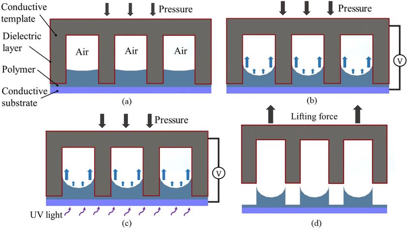
Vol. 27, No. 4 | 18 Feb 2019 | OPTICS EXPRESS A27

micro-hole array was fabricated by conventional photolithography and wet etching. The
diameter and arrangement of the MLA are determined by the design of the micro-holes array
in the template. Their AR can be precisely controlled by the electric field. In order to provide
enough space for the deformation of liquid polymer, the micro-holes depth should be much
larger than the thickness of the polymer layer and was therefore set to 50 µm. A 600 nm thick
dielectric silicon dioxide layer was subsequently formed on the template surface by thermal
oxidation so as to enhance the electric field strength [47–49]. Before the electrowetting
process, fluoroalkyl silane alcohol solution (Trichloro(1H,1H,2H,2H-perfluorooctyl) silane)
was spin coated on the surface of the template and dried as an anti-adhesion layer. Then
voltage was applied between the template and the conductive substrate to create an electric
field that changes the curvature of the meniscus polymer surface in the hole array, as shown
in Fig. 1(b). The voltage was driven by a waveform generator (Agilent 33250A) and a high
voltage power supply (Trek Model 610E). While pressure and voltage were maintained, UV
light was irradiated from the ITO coated glass substrate side to cure the polymer, as shown in
Fig. 1(c). Finally, the conductive silicon template was separated from the ITO glass substrate
and concave MLA films were obtained, as shown in Fig. 1(d). In order to generate replicas
after the fabrication of the MLA film, polydimethylsiloxane (PDMS, Dow Corning 184) was
spin-coated on the MLA film and separated after curing as a negative imprint template. By
using the PDMS negative mold to soft imprint a UV curable polymer layer (Norland optical
adhesive 65), multiple copies of the MLA film were reobtained facilely. In this method, the
structured silicon template can be re-used to fabricate MLA with different ARs by simply
changing the conditions of the applied electrical field, thereby limiting the cost of the process.

         Fig. 1. Schematic illustration of concave MLA fabrication by the electrowetting process. (a)
         Coating of a polymer layer on the bottom transparent conductive oxide substrate and contact of
         the micro-patterned template onto the polymer layer with a certain pressure to confine the
         polymer in the micro-holes; (b) Application of a voltage between the template and the
         conductive substrate under controlled pressure; (c) UV irradiation from the transparent
         conductive oxide substrate side to cure the polymer; (d) Separation of the template from the
         cured polymer.
Vol. 27, No. 4 | 18 Feb 2019 | OPTICS EXPRESS A28
2.2 Simulation methodology
2.2.1 Electrowetting simulations
The fabrication process was simulated using the finite element method (FEM) implemented in
a commercial software (COMSOL Multiphysics version 5.3).
For that purpose, we used a fluid mechanics model and an electric field model to describe
the fluid motion during the electrowetting process. According to the electro-hydrodynamics
principle, the movement of a fluid in an electric field can be described by the Navier−Stokes
equation of momentum and mass conservation [50]:
∂u 2 1
∂t + ρ u ∇u = −∇p + h∇ u + 3 h∇ ( ∇u ) + f + ρ g
ρ e
’ (1)
∂ρ + ∇ ( ρ u ) = 0
∂t
where ρ and η denote the fluid’s mass density and viscosity, respectively, p is the hydraulic
pressure in the fluid, f denotes the volumetric force generated by an electric field, u is the
e
fluid flow rate, g is gravitational acceleration and t represents time. The equation of motion
sets the fluid flow in the model as non-compressible with momentum conservation.
According to Maxwell's equation, the volumetric force f e has mainly three manifestations:
Coulomb force, electrostrictive force, and dielectrophoresis (DEP) force. DEP force is the
force which is exerted on a dielectric material when it is subjected to a non-uniform electric
field. Because the fluid used in this study is a dielectric polymer that has no free charge and
the electric field strength is insufficient to generate noticeable electrostrictive forces, the
electric volumetric force formula can be simplified to:
1
f e = − E 2 ∇ε (2)
2
where E represents the electric field intensity and ε represents the fluid’s dielectric constant.
In an electric field, the liquid molecules experience electric polarization. In a uniform electric
field, polarization molecules are evenly distributed and offset each other without showing
DEP force. In a non-uniform electric field, the distribution of polarization molecules is
directional. The DEP forces of molecules cannot offset each other and always point in the
direction of the stronger electric field region. In addition, the representation of the liquid
interface layer was described by a troposphere in this study, and is described by the basic
phase function ϕ [51,52]. According to Eq. (2), the electric volumetric force f e is only
concentrated at the gas-liquid interface as the gradient of the dielectric constant ε of the
polymer-air system varies greatly in this region.
In our simulation model, the thickness of the dielectric layer was set to 0.6 μm, as
measured experimentally, and the minimum distance between the template and the substrate
to 2 μm. Lastly, the polymer volume was fixed. The DEP force distribution and the motion of
the polymer were simulated under varying voltages of 60 V, 120 V and 180 V.
2.2.2 Ray tracing simulations
Light transmission through the MLA films was simulated using the commercial software
LightTools (Synopsys). The schematic diagram of the optical simulations is shown in Fig.
2(a). In our model, 108 parallel rays are incident on the patterned side of the MLA films and
one-period unit is illuminated, as depicted in the close-up shown in Fig. 2(b). The actual 3D
morphology of the MLA film is extracted from laser scanning confocal microscope to
establish a realistic model based on concave micro-lenses with a diameter of 20 µm and on a
Vol. 27, No. 4 | 18 Feb 2019 | OPTICS EXPRESS A29

hexagonal arrray with a pitchh of 30 µm. Th he hemisphericcal detector surrrounds the filmm and the
light intensity
              y distribution is obtained. Owwing to the sym  mmetric distribbution of the M
                                                                                          MLA, the
simplificationn does not affect the simulatiion accuracy. T The refractive index of the MMLA film
is set to 1.524
              4, which corressponds to the reefractive indexx value of NOAA65.

         Fig. 2.
               2 (a) Schematic illustration
                                  i           of thee ray-optics simullations frameworkk. Parallel light iss
         incideent to the patterneed side of the ML LA films, and thee transmitted lightt is captured by a
         hemisspherical detectorr. (b) Simulated unit cell of thee concave MLA        A with hexagonall
         arranggement (left), and
                                d corresponding sccanning electron m  microscope imagee of the fabricatedd
         MLA at a tilt angle of 45°(right).
                                 4

2.3 Characte
           erizations
The MLA film  ms fabricated in
                            i this study were
                                          w     applied to a CCT-tunablle LED lamp fo for optical
measurement.. The structuree of the CCT-tu unable LED ussed in this studdy is shown in Fig. 3(a).
The size of th
             he plate is 18 mm
                            m x 24 mm. The   T LED systeem consists off a ring-shapedd (4.3 mm
inner radius, 7.5 mm outer radius) cool-w white area and a circular (R = 3.9 mm) waarm-white
area inside the ring. The coool-white area is
                                            i made up of bblue light LEDD chips encapssulated by
7.85 wt% yelllow YAG pho    osphor with thhe peak emittinng wavelengthh of 533 nm annd 0.65%
wt% red YAG   G phosphor wiith peak emittiing wavelengthh of 625 nm aand has a CCT   T between
6200 and 6500 K. The warm-white
                           w             areea is encapsullated with 10.96 wt% yelloow YAG
phosphor with h peak emitting
                            g wavelength of o 533 nm andd 2.35% red YA   AG phosphor w with peak
emitting waveelength of 630 nm, and its CC  CT is betweenn 2500 and 28000 K. The LED  D chips of
these two areaas are driven separately
                            s          and the CCT can bbe controlled cconveniently frrom 2500
K to 6500 K by adjusting th he ratio of the driven currentts of the two aareas. The CCTT-tunable
LED is moun  nted on an alumminum fin to reeduce the effecct of LED juncction temperatuure on the
measurement,, as shown in Fig. 3(b). The schematic diaagram of the C    CCT-tunable LLED lamp
packaged with h MLA film is shown in Fig. 3(c).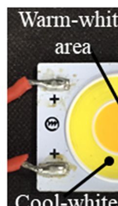
Vol. 27, No. 4 | 18 Feb 2019 | OPTICS EXPRESS A30
Fig. 3.
3 (a) Photograph of CCT-tunable chipc on board LE
ED. (b) CCT-tunabble LED mountedd
with aluminum
a fins. (c)) Schematic diagrram of CCT-tunabble LED lamp pacckaged with MLA
A
film. (d)
( Image of homee-made CCT distriibution measuremeent system.
A laser sccanning confoccal microscopee (Olympus LE EXT OLS40000) was used too measure
the geometries of the ML LA surface formed
f using different elecctrical parameeters. An
ultraviolet-vissible spectromeeter (Beijing Puxi,
P TU-1901)) was used to characterize thhe overall
(specular and diffuse) transm mittance and thhe haze (fractioon of diffused transmitted ligght to the
mitted light) off the MLA film
overall transm ms. Light was incident on thhe MLA side aat normal
direction and the spectra weere acquired fro om 450 nm to 780 nm. In thhe ACU measuurement, a
home-made teest system wass used to obtaiin the CCT disstribution, as sshown in Fig. 3(d). The
luminous flux x values at diffferent CCT rannges, powered by a Keithleyy 2450 DC souurce, were
measured by a 0.5 m integraating sphere co oupled to a specctrometer (Otsuuka LE5400)
3. Results and
a discussio
on
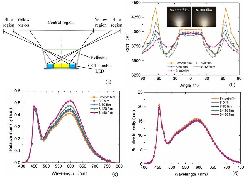
To explore the influence of the electrical parameters
p on tthe microlensees profile, we ffabricated
MLA films un nder different voltages and frequencies.
f Thhe influence off the applied vvoltage on
the MLA mo orphology was first investigated. Figure 4(a) shows tthe MLA film m surface
contours undeer different con nstant voltage, resulting in AAR values of 0..057 (0V), 0.3000 (60V),
0.366 (120V) and 0.373 (18 80V). In the abbsence of appliied voltage, thee surface contoour of the
MLA is nearrly flat. Undeer applied voltage, the conttour curvaturee of the MLA A surface
increases andd starts saturating at 180 V. ThisT saturationn is caused by the charges trrapped by
the dielectric layer. The eleectrical polarizaation charges iin the liquid wwill enrich at thhe liquid-
solid interfacee under an exteernal electric fiield. When the voltage is too high, the chargges in the
liquid will staart to cross the interface and enter the condu ductive templatte like a slight dielectric
breakdown, which
w weakens the electric po otential of the interface [53].. Therefore, the contour
curvature of MLA
M does not evolve anymo ore above 180 V and the maxximum AR vallue that is
achieved is 0.373.
To furtherr increase the saturation valu ue of the appllied voltage, sqquare wave vooltages at
different frequ uencies were applied
a during the fabricatioon process as sshown in Fig. 44(b). The
corresponding g AR obtained d are 0.366 (0Hz), 0.503 (1H Hz), 0.547 (5HHz), 0.603 (255Hz) and
0.263 (125Hzz). Compared with w constant voltages,
v squaree wave voltagees between 1 aand 25 Hz
produce a larger sag heightt. Indeed, when n the external voltage exceedds the saturation value,
the charge en nters the dieleectric layer, fo
orming a reverrse electric fieeld. Because tthere is a
certain hysterresis in the charge migration n, when the appplied voltage reverses, the electrons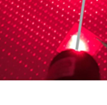
Vol. 27, No. 4 | 18 Feb 2019 | OPTICS EXPRESS A31

need time to migrate in reverse. Before the charges finish migrating, the reverse electric field
and the external electric field form a short-term codirectional superposition, making the
electric field stronger than in the saturated state [53]. Under a certain frequency of reversing,
the superposition electric field can maintain a stable value that is higher than the pristine
saturation voltage, so the contour curvature formed under the square wave voltage condition
is larger.
     Owing to the better smoothness and sag height of the MLA produced, 5 Hz was selected
as the frequency for the next tests. Figure 4(c) shows the contour comparison of the MLA
formed under different 5 Hz square wave voltages. The resulting AR value are 0.057 (0V),
0.212 (60V), 0.547 (120V) and 0.693 (180V). As previously described, the surface curvature
gradually increases with increasing voltage amplitude and reaches a maximum AR of 0.693.
Compared with the constant voltage of the same magnitude, square wave voltage provides
higher saturation voltages and achieves higher sag heights. By regulating the square wave
voltage amplitude, the AR of the MLA can be tuned over a broad range. In the following, we
refer to the planar polymer film as the “Smooth Film”, and to the concave MLA films formed
by a square wave voltage of 0 V, 60 V, 120 V and 180 V as “S-0 film”, “S-60 film”, “S-120
film”, and “S-180 film”, respectively. The macroscopic and microscopic images of S-0 film
and S-180 film are shown in Fig. 4(d). It can be clearly seen that the AR of the S-180 film is
significantly larger than S-0 film and the MLA has good spatial homogeneity.
     Details on the DEP force distribution and the morphology variation obtained from FEM
simulations are shown in Fig. 4(e). The DEP forces concentrate at the surface of the polymer.
The DEP force is close to zero in the central region and gradually increases towards the
edges. By increasing the applied voltage, the DEP forces get higher on the polymer surface,
thus increasing the AR of the MLA. The polymer surface in the initial state is almost flat. The
DEP force vectors are shown by the white arrows in the insets of Fig. 4(e). As the DEP force
is much larger in the edge regions and since the polymer volume is conserved, the edge
regions are pulled upward, while the central region is forced down, finally forming a structure
with parabolic shape.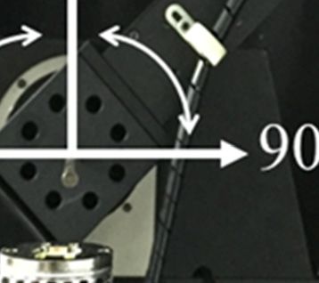
Vol. 27, No. 4 | 18 Feb 2019 | OPTICS EXPRESS A32

Fig. 4. (a) MLA film surface contour at different constant voltages. (b) MLA surface contour
for different square wave frequencies at 120 V (c) MLA surface contour for different square
wave voltages at 5 Hz. (d) Photographs (left) and scanning electron microscope images (right,
taken under 45° tilt angle) of the S-0 and S-180 films. The size of the patterned area is 20 mm
× 20 mm. (e) Simulated DEP force distribution along the meniscus polymer surface for
different applied voltages. The insets show the initial state (left) and the final state (right) of
the polymer meniscus at 180 V.
Vol. 27, No. 4 | 18 Feb 2019 | OPTICS EXPRESS A33

         Fig. 5.
               5 (a) Overall trannsmittance and (b) haze (in transm mission) spectra off the smooth film
                                                                                                       m
         plotted together with the
                                 t spectra of th he S-0, S-60, S-1 20 and S-180 fillms. (c) Far-fieldd
         transmmission pattern of a 650 nm laser beeam irradiating thee S-180 film. (d) Simulated angularr
         distrib
               bution of the tran
                                nsmitted light rays based on the m  measured morphollogies obtained att
         differeent voltages.

    Further, we
              w evaluated th   he optical propperties of the rresulting light diffusing film
                                                                                           ms. Figure
5(a) shows the measured ov    verall transmittaance of MLA ffilms. The trannsmittance valuues of the
structured filmm formed at eache     voltage arre slightly low
                                                             wer than for thhe smooth film  m, but the
average transm  mittance exceeeds 89%. Figu   ure 5(b) showss the measuredd haze (in transsmission)
of the MLA films.
               f       As the forming
                               f         voltag
                                              ge increases, thhe haze valuess of the films gradually
increase fromm 1.6% (0 V) to   o 48.7% (180 V).V The increaase in haze is ccaused by the rrefraction
of the MLA. When light iss incident on the structured surface, it is nnormally refraccted by a
large angle according
              a            to Snell’s law. With
                                            W higher currvature, the reefraction effectt is more
pronounced, thust     enhancing g the haze vallues of the fillms, namely thheir diffusion property.
Illuminating a laser beam on MLA film        m samples show    ws the scatterring performannce more
intuitively, ass shown in Fig  g. 5(c). Under the concave sstructure, the llaser beam is dispersed
into a hexagon  nal array of spots, underlyingg the good scatttering ability oof the S-180 fillm.
    To furtherr study the scaattering mechan   nism of light bby MLA films, ray optics sim   mulations
were perform med out of realistic MLA mo      orphologies. Ass shown in Figg. 5(d), all thee samples
have a high light
               l      intensity peak at 0° beecause of the relatively largge spacing bettween the
microlenses. InI the enlarged  d view, we seee that the transsmitted light eexit angle of S--0 film is
less than 9° an nd distributes mainly in the central
                                               c       region. On the other hhand, the lightt intensity
distribution of the DEP forcce-shaped samp     ples not only cconcentrates inn the central reegion, but
also forms a second
               s        peak at a higher angular range. As thhe applied volttage increases,, the peak
value of the second peak low   wers and the an ngular spread iincreases. The maximum exitt angle of
transmitted ligght of the S-60 0 film, S-120 film,
                                              f      and S-1800 film is foundd to be 9°, 25°° and 34°,
Vol. 27, No. 4 | 18 Feb 2019 | OPTICS EXPRESS A34

respectively. This demonstrates that the increase of AR of the MLA surface can more evenly
scatter the light into a wider angular range.

         Fig. 6. (a) Schematic of the light distribution in a CCT-tunable LED lamp. (b) Angle-
         dependent CCT distribution of the lamps covered with the smooth film and with the MLA
         films. The insets show the photographs of the light spots obtained with a CCT-tunable LED
         with smooth film (left) and with the S-180V film (right). (c) Emission spectra of different films
         at the zenith angles of 65°. (d) Emission spectra of the corresponding samples measured with
         an integrating sphere.

    As the fabricated MLA exhibit a high optical transmittance and broaden the angular
distribution of transmitted light, they are relevant candidates to improve light management in
CCT-tunable LEDs. Figure 6(a) shows a schematic diagram of the light distribution of the
CCT tunable LED. The LED is surrounded by a cylindric reflector as desired for practical
applications. In the center region above the lamp, the CCT values are uniform because the
rays from the warm-white and cold-white areas are not blocked and can be mixed well. In the
yellow region the light coming from the cool-white area (located near the reflector), is
blocked and cannot transmit to this region. In this part, warm-white light mostly dominates
and the CCT is low, resulting in the appearance of a yellow halo. In the blue region, the light
from the warm-white area is also shielded, and only the light from cool-white area, which is
away from the reflector, illuminates this area. Thus, the CCT of this area is significantly
higher than other angles and a blue ring appears.
    In view of the light scattering properties of MLA films, we covered the MLA film
samples at the top of the CCT-tunable LED lamp for an ACU improvement demonstration.
As shown in Fig. 6(b), the CCT curve of the lamp has a large fluctuation when covered with a
smooth film. We define the difference between the maximum and minimum CCT values as
the CCT deviation, which is as high as 791 K in the smooth film. As the AR of the MLA
increases, the CCT deviation of the lamp gradually decreases. Thus, the CCT deviation of the
S-180 film configuration is reduced to 357 K. The improvement of the ACU of the lamp is
mainly caused by the CCT decrease at a zenith angle of 65°. In other words, it relieves the
Vol. 27, No. 4 | 18 Feb 2019 | OPTICS EXPRESS A35
blue ring phenomenon. Assisted by the MLA film, the emitting light is refracted and mixed
more evenly and more light rays from the warm-white area enter the blue region. Therefore,
the CCT at an angle of 65° gradually decreases as the AR of the MLA film increases. The
inset shows the light spot patterns of the CCT-tunable LED with the smooth film (left) and
the S-180 film (right). It is obvious that the former has a clear blue ring and a yellow halo.
The latter has no obvious blue ring and the yellow halo is also significantly reduced.
To verify the analysis regarding the disappearance of the blue ring phenomenon, we
extracted and compared the emission spectra for the different configurations considered and
for a zenith angle of 65° (see Fig. 6(c)). These spectra display little difference in the peaks of
the blue light band (400 nm–500 nm). The enhancement of scattering performance has less
effect on the blue light. On the other hand, these measurements indicate significant
differences in the yellow portion of the spectra. With increasing applied voltage, the peaks
and relative intensity of the yellow light (500 nm–750 nm) spectrum gradually increase. Films
with a higher haze (higher AR, see Fig. 5(b)) have a better light diffusing property and more
warm-white light can reach the spatial range of 65° which has an overall effect of lowering
the resulting CCT at high zenith angles, as observed in Fig. 6(b).
To investigate the influence of the MLA film on the luminous flux, we used an integrating
sphere to measure the emission spectrum of the CCT-tunable LED lamp covered with the
different films. The driven current is the same as for the ACU measurement and the results
are shown in Fig. 6(d). The emission intensity of the CCT-tunable LED lamp upon integration
of the MLA films is just slightly lower than by using the smooth film, in accordance with the
transmittance values reported in Fig. 5(a). Thus, the maximum luminous flux loss ratio
amounts to 4.53% when the lamp is covered with S-180 film and with respect to the smooth
film configuration.
In practical applications, CCT-tunable LED lamps need to be adjusted to different CCT
ranges according to requirements. To this end, we validated the research results in different
CCT ranges. Table 1 lists the CCT deviations and luminous fluxes of CCT-tunable LEDs
covered by smooth film and S-180V film over the full CCT range of 2500–6500 K. From the
CCT deviation comparison, it is found that as the average CCT value increases, the CCT
deviation gradually increases. In each CCT range, the CCT deviation of the S-180V film lamp
is significantly reduced compared with the smooth film configuration, which improves the
ACU of the LED efficiently. In terms of luminous flux, the lamps covered with S-180V film
have slightly narrower CCT range than smooth film, and the decreasing ratio is within 5%.
Therefore, the MLA films can effectively improve the ACU of CCT-tunable LEDs and
maintain a high luminous flux, which meets the needs of practical applications.
Table 1. Correlated color temperature deviation (ΔCCT) and luminous flux of CCT-
tunable LED covered with a smooth film and with the S-180V film for different CCT
ranges. The uncertainties of the CCT deviation and luminous flux data were derived out
of 3 and 5 measurements, respectively.
ΔCCT (K) Luminous Flux (lm)
CCT Range (K)
Smooth film S-180V film Smooth film S-180V film
2500-3000 454 ± 4 214 ± 4 421.6 ± 0.3 403.9 ± 0.1
3000-4000 772 ± 3 339 ± 2 466.4 ± 0.2 447.2 ± 0.1
4000-5000 791 ± 6 357 ± 3 478.0 ± 0.3 456.4 ± 0.3
5000-6000 997 ± 8 616 ± 7 470.1 ± 0.1 452.7 ± 0.2
6000-6500 1206 ± 14 771 ± 9 472.6 ± 0.2 452.3 ± 0.2Vol. 27, No. 4 | 18 Feb 2019 | OPTICS EXPRESS A36
4. Conclusion
In summary, we have presented a novel approach that exploits the electrowetting effect to
fabricate MLA with tunable ARs for CCT-tunable LED applications. At the optimized
voltage frequency of 5 Hz, the AR of the MLA gradually increases from 0.057 to 0.693 by
increasing the applied voltage from 0 V to 180 V, which leads to higher DEP forces. As
confirmed experimentally and numerically, the MLA films with higher AR exhibit a higher
haze and a broader angular light distribution. When the MLA films are applied to a CCT-
tunable LED with a CCT of 3000-4000 K, the CCT deviation is largely reduced and the best
ACU performance is achieved with the S-180 MLA film, which has the highest AR of 0.693
among all the fabricated MLA. The S-180 film also shows a remarkable performance for
ACU improvement in other CCT ranges and helps to maintain a good lumen output. The
ACU enhancement is caused primarily by the homogenous mixing of the warm and of the
cool light, caused by the high diffusing property of the MLA film. Our method for the
fabrication of MLA with tailorable ARs is facile, rapid and cost-effective. Higher
improvements in ACU performances are expected by further optimizing the MLA design,
especially by reducing the spacing between the micro-lenses.
Funding
National Natural Science Foundation of China (NSFC) (51805173, 51735004 and
U1401249); Natural Science Foundation of Guangdong Province (2014A030312017); The
Fundamental Research Funds for the Central Universities (2018MS44); Karlsruhe School of
Optics & Photonics (KSOP)
Acknowledgments
The authors would like to thank Shudong Yu at South China University of Technology for his
guidance and for making this collaboration possible. They also acknowledge Prof. Jinyou
Shao, Prof. Xiangming Li and Prof. Hongmiao Tian at Xi'an Jiaotong University for
experimental guidance and helpful discussions.
References
1. T. F. Zhu, Z. Liu, Z. Liu, F. Li, M. Zhang, W. Wang, F. Wen, J. Wang, R. Bu, J. Zhang, and H. X. Wang,
“Fabrication of monolithic diamond photodetector with microlenses,” Opt. Express 25(25), 31586–31594
(2017).
2. J. D. Myers, W. Cao, V. Cassidy, S. H. Eom, R. Zhou, L. Yang, W. You, and J. Xue, “A universal optical
approach to enhancing efficiency of organic-based photovoltaic devices,” Energy Environ. Sci. 5(5), 6900–6904
(2012).
3. X. Zhou, Y. Peng, R. Peng, X. Zeng, Y. A. Zhang, and T. Guo, “Fabrication of large-scale micro-lens arrays
based on screen printing for integral imaging 3D display,” ACS Appl. Mater. Interfaces 8(36), 24248–24255
(2016).
4. H. Y. Lin, Y. M. Pai, J. X. Shi, X. Y. Chen, C. H. Lin, C. M. Weng, T. Y. Chen, C. C. Lin, M. D. B. Charlton, Y.
P. Huang, C. H. Chen, H. P. Chen, and H. C. Kuo, “Optimization of nano-honeycomb structures for flexible w-
LEDs,” Opt. Express 25(17), 20466–20476 (2017).
5. X. Luo, R. Hu, S. Liu, and K. Wang, “Heat and fluid flow in high-power LED packaging and applications,” Pror.
Energy Combust. Sci. 56, 1–32 (2016).
6. Y. U. Shudong, Y. Tang, L. I. Zongtao, K. Chen, X. Ding, and Y. U. Binhai, “Enhanced optical and thermal
performance of white light-emitting diodes with horizontally layered quantum dots phosphor nanocomposites,”
Photon. Res. 6(2), 90 (2018).
7. S. Yu, Y. Tang, Z. Li, Y. Chen, B. Yu, and G. Liang, “Freeform illumination lens design combining energy and
intensity mapping,” Opt. Eng. 56(4), 045101 (2017).
8. X. Ding, M. Li, Z. Li, Y. Tang, Y. Xie, X. Tang, T. Fu," Thermal and optical investigations of a laser-driven
phosphor converter coated on a heat pipe," App. Thermal Engin. 148, 1099-1106 (2019).
9. Y. Peng, Y. Mou, Y. Zhuo, H. Li, X. Z. Wang, M. X. Chen, and X. B. Luo, “Preparation and luminescent
performances of thermally stable redemitting phosphor-in-glass for high-power lighting,” J. Alloys Compd. 768,
114–121 (2018).
10. J. S. Li, Y. Tang, Z. T. Li, X. R. Ding, L. S. Rao, and B. H. Yu, “Effect of Quantum Dot Scattering and
Absorption on the Optical Performance of White Light-Emitting Diodes,” IEEE Trans. Electron. Dev. 65, 2877–
2884 (2018).Vol. 27, No. 4 | 18 Feb 2019 | OPTICS EXPRESS A37
11. Z. Huai, L. Sheng, and L. Xiaobing, “Enhancing Angular Color Uniformity of Phosphor-Converted White Light-
Emitting Diodes by Phosphor Dip-Transfer Coating,” J. Lightwave Technol. 31(12), 1987–1993 (2013).
12. S. Yu, B. Zhuang, J. Chen, Z. Li, L. Rao, B. Yu, and Y. Tang, “Butterfly-inspired micro-concavity array film for
color conversion efficiency improvement of quantum-dot-based light-emitting diodes,” Opt. Lett. 42(23), 4962–
4965 (2017).
13. L. Rao, Y. Tang, Z. Li, X. Ding, J. Li, S. Yu, C. Yan, and H. Lu, “Effect of ZnO nanostructures on the optical
properties of white light-emitting diodes,” Opt. Express 25(8), A432–A443 (2017).
14. Y. Tang, Z. Li, Z.-T. Li, J.-S. Li, S.-D. Yu, and L.-S. Rao, “Enhancement of Luminous Efficiency and
Uniformity of CCT for Quantum Dot-Converted LEDs by Incorporating With ZnO Nanoparticles,” IEEE Trans.
Electron Dev. 65(1), 158–164 (2018).
15. J.-S. Li, Y.-H. Chen, Z.-T. Li, S.-D. Yu, Y. Tang, X.-R. Ding, and W. Yuan, “ACU Optimization of pc LEDs by
Combining the Pulsed Spray and Feedback Method,” J. Disp. Technol. 12(10), 1229–1234 (2016).
16. J.-S. Li, C.-M. Yan, Z.-T. Li, G.-W. Liang, Y. Tang, and B.-H. Yu, “Color Uniformity Enhancement for WLEDs
Using Inverted Dispensing Method,” IEEE Photonics Technol. Lett. 29(23), 2079–2082 (2017).
17. Y. Tang, G. Liang, J. Chen, S. Yu, Z. Li, L. Rao, and B. Yu, “Highly reflective nanofiber films based on
electrospinning and their application on color uniformity and luminous efficacy improvement of white light-
emitting diodes,” Opt. Express 25(17), 20598–20611 (2017).
18. H. C. Kuo, C. W. Hung, H. C. Chen, K. J. Chen, C. H. Wang, C. W. Sher, C. C. Yeh, C. C. Lin, C. H. Chen, and
Y. J. Cheng, “Patterned structure of remote phosphor for phosphor-converted white LEDs,” Opt. Express 19(S4
Suppl 4), A930–A936 (2011).
19. S. Yu, Z. Li, G. Liang, Y. Tang, B. Yu, and K. Chen, “Angular color uniformity enhancement of white light-
emitting diodes by remote micro-patterned phosphor film,” Photon. Res. 4(4), 140 (2016).
20. Q. Chen, Z. Li, K. Chen, Y. Tang, X. Ding, and B. Yu, “CCT-tunable LED device with excellent ACU by using
micro-structure array film,” Opt. Express 24(15), 16695–16704 (2016).
21. A. Lee, H. Chen, S. C. Tan, and S. Y. R. Hui, “Precise Dimming and Color Control of Light-Emitting Diode
Systems based on Color Mixing,” IEEE Trans. Power Electron. 2015, 1 (2015).
22. A. T. L. Lee, J. K. O. Sin, and P. C. H. Chan, “Scalability of Quasi-Hysteretic FSM-Based Digitally Controlled
Single-Inductor Dual-String Buck LED Driver to Multiple Strings,” IEEE Trans. Power Electron. 29(1), 501–
513 (2014).
23. C. Y. Liu, K. J. Chen, D. W. Lin, C. Y. Lee, C. C. Lin, S. H. Chien, M. H. Shih, G. C. Chi, C. Y. Chang, and H.
C. Kuo, “Improvement of emission uniformity by using micro-cone patterned PDMS film,” Opt. Express 22(4),
4516–4522 (2014).
24. J. Yong, F. Chen, Q. Yang, G. Du, H. Bian, D. Zhang, J. Si, F. Yun, and X. Hou, “Rapid fabrication of large-
area concave microlens arrays on PDMS by a femtosecond laser,” ACS Appl. Mater. Interfaces 5(19), 9382–
9385 (2013).
25. R. Ahmed, A. K. Yetisen, and H. Butt, “High Numerical Aperture Hexagonal Stacked Ring-Based Bidirectional
Flexible Polymer Microlens Array,” ACS Nano 11(3), 3155–3165 (2017).
26. J. Tan, M. Shan, C. Zhao, and J. Liu, “Design and fabrication of diffractive microlens arrays with continuous
relief for parallel laser direct writing,” Appl. Opt. 48, 340–345 (2008).
27. M. Severi and P. L. Mottier, “Etching selectivity control during resist pattern transfer into silica for the
fabrication of microlenses with reduced spherical aberrations,” Opt. Eng. 38(1), 146–150 (1999).
28. A. M. B. Stern and T. R. Jay, “Dry etching for coherent refractive microlens arrays,” Opt. Eng. 33(11), 3547–
3551 (1994).
29. Z. D. Popovic, R. A. Sprague, and G. A. Connell, “Technique for monolithic fabrication of microlens arrays,”
Appl. Opt. 27(7), 1281–1284 (1988).
30. J. Zhang, C. Wang, J. Zeng, and A. J. Pang, “A Low Cost Bumping Method for Flip Chip Assembly and MEMS
Integration,” IEEE Trans. Compon. Packag. Tech. 30(4), 781–786 (2007).
31. H. Jung and K. H. Jeong, “Monolithic polymer microlens arrays with high numerical aperture and high packing
density,” ACS Appl. Mater. Interfaces 7(4), 2160–2165 (2015).
32. C. Y. Chang, S. Y. Yang, L. S. Huang, and J. H. Chang, “Fabrication of plastic microlens array using gas-
assisted micro-hot-embossing with a silicon mold,” Infrared Phys. Technol. 48(2), 163–173 (2006).
33. D. Xie, X. Chang, X. Shu, Y. Wang, H. Ding, and Y. Liu, “Rapid fabrication of thermoplastic polymer refractive
microlens array using contactless hot embossing technology,” Opt. Express 23(4), 5154–5166 (2015).
34. X. J. Shen and L. Lin, Micro Plastic Embossing Process: Experimental and Theoretical Characterizations
(Springer Berlin Heidelberg, 2001).
35. M. Kuang, L. Wang, and Y. Song, “Controllable printing droplets for high-resolution patterns,” Adv. Mater.
26(40), 6950–6958 (2014).
36. J. Y. Kim, N. B. Brauer, V. Fakhfouri, D. L. Boiko, E. Charbon, G. Grutzner, and J. Brugger, “Hybrid polymer
microlens arrays with high numerical apertures fabricated using simple ink-jet printing technique,” Opt. Mater.
Express 1(2), 259–269 (2011).
37. R. Hünig, A. Mertens, M. Stephan, A. Schulz, B. Richter, M. Hetterich, M. Powalla, U. Lemmer, A. Colsmann,
and G. Gomard, “Flower Power: Exploiting Plants’ Epidermal Structures for Enhanced Light Harvesting in
Thin Film Solar Cells,” Adv. Opt. Mater. 4(10), 1487–1493 (2016).Vol. 27, No. 4 | 18 Feb 2019 | OPTICS EXPRESS A38
38. B. Fritz, R. Hünig, R. Schmager, M. Hetterich, U. Lemmer, and G. Gomard, “Assessing the influence of
structural disorder on the plant epidermal cells’ optical properties: a numerical analysis,” Bioinspir. Biomim.
12(3), 036011 (2017).
39. Y. Peng, Y. Mou, X. Guo, X. Xu, H. Li, M. Chen, and X. Luo, “Flexible fabrication of a patterned red phosphor
layer on a YAG:Ce3+ phosphor-in-glass for high-power WLEDs,” Opt. Mater. Express 8(3), 605 (2018).
40. Q. Xu, B. Dai, Y. Huang, H. Wang, Z. Yang, K. Wang, S. Zhuang, and D. Zhang, “Fabrication of polymer
microlens array with controllable focal length by modifying surface wettability,” Opt. Express 26(4), 4172–4182
(2018).
41. C. Fang, J. Zheng, Y. Zhang, Y. Li, S. Liu, W. Wang, T. Jiang, X. Zhao, and Z. Li, “Antireflective Paraboloidal
Microlens Film for Boosting Power Conversion Efficiency of Solar Cells,” ACS Appl. Mater. Interfaces 10(26),
21950–21956 (2018).
42. Y. Peng, X. Guo, R. Liang, Y. Mou, H. Cheng, M. Chen, and S. Liu, “Fabrication of Microlens Arrays with
Controlled Curvature by Micromolding Water Condensing Based Porous Films for Deep Ultraviolet LEDs,”
ACS Photonics 4(10), 2479–2485 (2017).
43. B. Yang, J. Zhou, Q. Chen, L. Lei, and K. Wen, “Fabrication of hexagonal compound eye microlens array using
DMD-based lithography with dose modulation,” Opt. Express 26(22), 28927–28937 (2018).
44. X. Li, Y. Ding, J. Shao, H. Liu, and H. Tian, “Fabrication of concave microlens arrays using controllable
dielectrophoretic force in template holes,” Opt. Lett. 36(20), 4083–4085 (2011).
45. X. Li, Y. Ding, J. Shao, H. Tian, and H. Liu, “Fabrication of microlens arrays with well-controlled curvature by
liquid trapping and electrohydrodynamic deformation in microholes,” Adv Mater 24, OP165–169, OP190
(2012).
46. M. Vallet, B. Berge, and L. Vovelle, “Electrowetting of water and aqueous solutions on poly(ethylene
terephthalate) insulating films,” Polymer (Guildf.) 37(12), 2465–2470 (1996).
47. X. Li, J. Shao, H. Tian, Y. Ding, and X. Li, “Fabrication of high-aspect-ratio microstructures using
dielectrophoresis-electrocapillary force-driven UV-imprinting,” J. Micromech. Microeng. 21(6), 065010 (2011).
48. X. Li, H. Tian, J. Shao, Y. Ding, and H. Liu, “Electrically modulated microtransfer molding for fabrication of
micropillar arrays with spatially varying heights,” Langmuir 29(5), 1351–1355 (2013).
49. X. Li, H. Tian, Y. Ding, J. Shao, and Y. Wei, “Electrically templated dewetting of a UV-curable prepolymer film
for the fabrication of a concave microlens array with well-defined curvature,” ACS Appl. Mater. Interfaces
5(20), 9975–9982 (2013).
50. H. Tian, J. Shao, Y. Ding, X. Li, and X. Li, “Numerical studies of electrically induced pattern formation by
coupling liquid dielectrophoresis and two-phase flow,” Electrophoresis 32(17), 2245–2252 (2011).
51. D. Jacqmin, Calculation of Two-Phase Navier–Stokes Flows Using Phase-Field Modeling (Academic Press
Professional, Inc., 1999).
52. C. Zhou, P. Yue, J. J. Feng, C. F. Ollivier-Gooch, and H. H. Hu, “3D Phase-Field Simulations of Interfacial
Dynamics in Viscoelastic Fluids with Adaptive Meshing,” in 61st Annual Meeting of the APS Division of Fluid
Dynamics (2008).
53. X. Li, H. Tian, J. Shao, Y. Ding, X. Chen, L. Wang, and B. Lu, “Decreasing the Saturated Contact Angle in
Electrowetting-on-Dielectrics by Controlling the Charge Trapping at Liquid-Solid Interfaces,” Adv. Funct.
Mater. 26(18), 2994–3002 (2016).You can also read