Optical evolution through integration - www.vlcphotonics.com January 2014
←
→
Page content transcription
If your browser does not render page correctly, please read the page content below
Optical evolution through integration

                January 2014

           www.vlcphotonics.com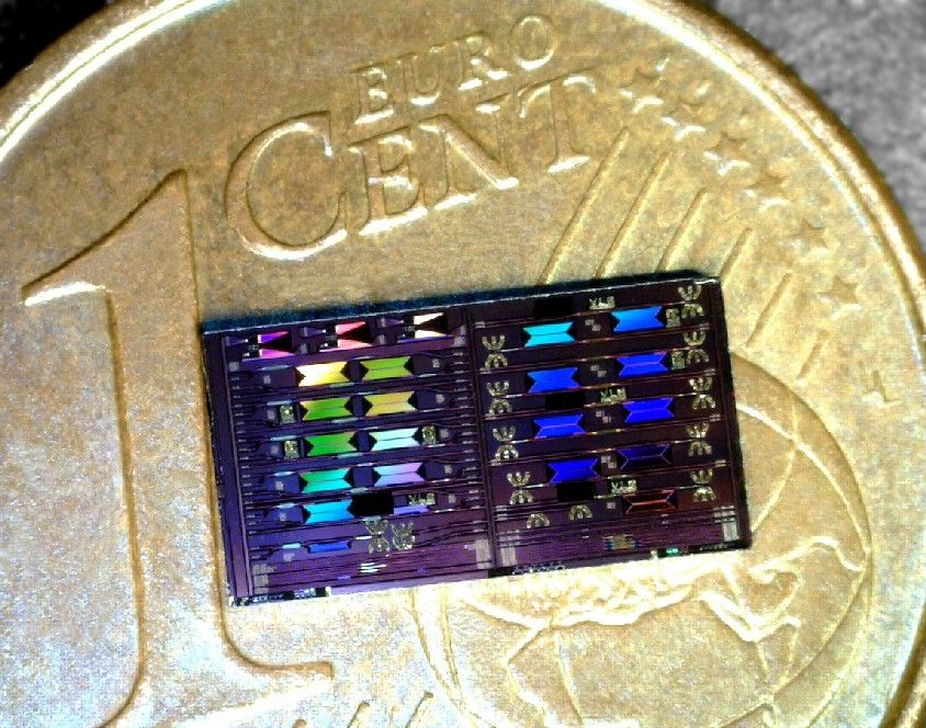
Company Introduction

• Optical chip design in multiple photonic technologies

• UPV spin-off, presence in Spain and the Netherlands

• 7 members of extensive academic and industrial experience

• 10+ years in the field of integrated optics and photonics

 02/27/14                         www.vlcphotonics.com        2
What does photonic integration mean?

      Aggregate multiple components of a system into a single monolithic chip.

                                                                            Transistors
                                                                            Capacitors
                                                                            Resistors
                                                                            Inductors
                                                                            etc.

           Same evolution path as electronics:
                                  Lasers/LEDs
                                  Photodetectors
                                  Modulators
                                  Optical Filters
                                  Couplers/Splitters
                                  Multiplexers
                                  Interferometers
                                  etc.                     Micro-optics

                                                                     Integrated optics
02/27/14                        www.vlcphotonics.com                               3
Applications and Markets

           Communications                            Signal Processing
                                                     • Optical Metrology
           • FTTx and Access Networks
                                                     • Optical Instrumentation
           • Microwave/RF Photonics
                                                     • Astrophotonics
           • Long-haul and transport networks
                                                     • Quantum Optics/QKD
           • Optical Datacom

                Fiber Sensing                              BioPhotonics
                • Structural Engineering                   • Medical Instrumentation
                • Chemical Sensors                         • Photonic Lab-on-a-Chip
                • Transport and Aerospace                  • Analytics and Diagnostics
                • Energy and Utilities                     • Optical Biosensors

02/27/14                            www.vlcphotonics.com                                 4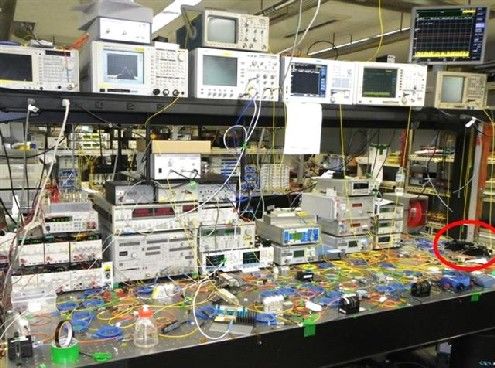
Photonic Integration: Why?

Advantages of chip integration:
    – Reduced volume and weight
    – Simpler assembly and packaging
    – Better mechanical and thermal stability
    – Enable complex system scalability
    – Allow to scale up production
    – Reduce costs on large series

     System
                          Chip Design              Manufacture and test
    Concept

Mimic the electronic
  fabless model          Design houses              Generic foundries

02/27/14                    www.vlcphotonics.com                          5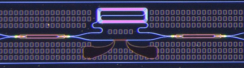
VLC Photonics activity

                     Custom design    and    Manufacture   of

                            application-specific

                     Photonic Integrated Circuits

      Largest            Cost effectively             Low-risk and fast
   technology &          through shared              prototyping due to
 foundry selection       manufacturing                proven expertise

02/27/14                  www.vlcphotonics.com                      6
Photonic integration: How?
                             System concept                          Packaging

C                                                                                                   F
                                                                                                    O
U                                                                            Chip testing           U
S
           Optical architecture
                                                                                                    N
T                                                                                                   D
                                                                                                    R
O                                                                          Manufacture

             Chip architecture                                                                      I
M                                                                                                   E
E                                                                                                   S
R                       Chip design                               Mask layout + DRC

                                                                                               PDKs +
                                         Performance simulation                             Licensed IP

                   2-8 weeks                                              4-8 months

             Total flexibility + Turn-key solution
02/27/14                               www.vlcphotonics.com                                     7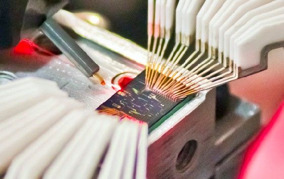
Multiple technologies
                      Depending on material technology:
                       - Silicon photonics: Silicon Dioxide (SiO2), Silicon-On-

                      Insulator (SOI), Silicon Nitride (Si3N4), etc.

                       - III-V semiconductors: Indium Phosphide (InP),
                      Gallium Arsenide (GaAs), etc.
                       - Lithium Niobate (LiNbO3)

    Best Technology Features                  SOI     SiO2/Si   Si3N4/SiO2   InP/GaAs   LiNbO3
                  Low propagation loss
                Good coupling to fibers
              Good electro-optic effect
              Good thermo-optic effect
        Good electro-absorption effect
        Light generation / regeneration
                          Small footprint
           Compatibility with electronics

                 Wavelength range:          ~1200-2000 nm (Si3N4: 400 – 2350 nm)

02/27/14                                www.vlcphotonics.com                                 8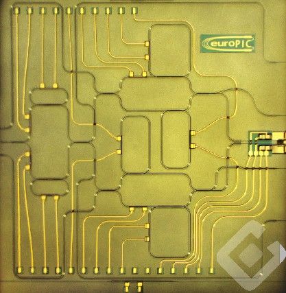
Part of our foundry network

02/27/14   www.vlcphotonics.com          9
Design and Test Infrastructure

–    Full photonic design framework, with several commercial

     software licenses and proprietary libraries.

–    OPCLUSTUX HPC simulation cluster (10 HP Proliant ML110

     servers, 2 Intel Xeon processors each, 40 GB RAM, 2 TB storage)

–    Access to a 4M€ optical communications lab, RF test

     up to 50 GHz, digital up to 40 Gb/s

–    Fully automated photonic characterization and test

     setups for bare chips in clean vaults.

–    Manual wire bonding and thermal testing capabilities

    02/27/14                               www.vlcphotonics.com        10
Added value
VLC Photonics designs in the best suited material technology and for
the most appropriate foundry.
VLC Photonics offers a proprietary library of photonic building blocks
with new or extended functionalities from the standard PDKs.
VLC Photonics aims for fast response and first-time-right fabrication
thanks to its long experience with its tools and partners.
VLC Photonics ensures confidentiality along the whole manufacturing
chain. NDA in place from start, customer's design IP transferred.
02/27/14 www.vlcphotonics.com 11Ex: Ultra-compact wavelength channel splitting
Miniature dual Arrayed Waveguide Grating (AWG) for wavelength channel
splitting system, to be used in optical telecom or in a fiber sensing system.
Photonic chip layout Manufactured SOI prototype
Optical system concept at ePIXfab MPW run, 2011
Fiber sensors
Mux/
Mux/
Interrogator demux
demux
Standard PLC vs. SOI AWG sizes
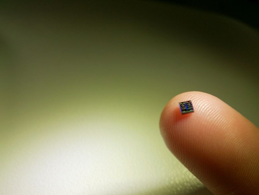
02/27/14 www.vlcphotonics.com 12Ex: Miniature fiber sensor interrogation
Fiber Bragg Grating (FBG) sensor interrogator, based on
AWG + 10 GHz Mach-Zehnder modulator + photodiode.
Read-out up to 100 kHz, spectral resolution below 10 pm.
Manufactured SOI prototypes, 2012
Equivalent fiber interrogator
size comparison
~10x smaller!
02/27/14 www.vlcphotonics.com 13Ex: Optimized photonic receiver
Using ring-assisted Mach-Zehnder interferometer filters
complementary acting as frequency discriminators, to
simplify on-chip detection with a balanced photodiode
for low-power MWP links.
Optical system concept
and chip architecture Photonic chip layout
Manufactured InP prototype, 2012
02/27/14 www.vlcphotonics.com 14Example: Next-gen optical network encoder
Novel OCDMA system using passive delay lines and parallel waveguide couplers.
Code tunability is achieved by the use of thermo optic heaters, which add phase
shifts to each sample. Prototyped in two different technologies.
TriPleX prototype
Optical system concept Photonic chip layout
at LioniX MPW run, 2011
SOI version, 2012
02/27/14 www.vlcphotonics.com 15Ex: Integrated Microwave Photonic Beamformer
Comparable bulk beamformer
Optical
system
concept
and chip
architecture
- World first silicon photonic MWPBF Manufactured SOI prototype
- Signal processing at 40 GHz at ePIXfab MPW run, 2011
- Precise relative phase tuning per branch (filter tap)
- Smallest foot print, near future merge with electronics
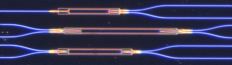
02/27/14 www.vlcphotonics.com 16Ex: Precise interferometric systems
Interferometers:
- Mach-Zehnder
- Michelson
- Sagnac
- ...
Excellent
accuracy vs.
fiber based
implementations
02/27/14 www.vlcphotonics.com 173D Photonic crystal structures - Automated pattern generation - Periodic structures - All kind of cell geometries and sizes - GDS/CAD ready for production Applications: - Lighting - Solar energy harvesting - Dielectric mirrors - Resonant cavities - Highly directional antennas - Non-linear effects - Lasing - Waveguides and junctions 9th April, 2012 www.vlcphotonics.com 18
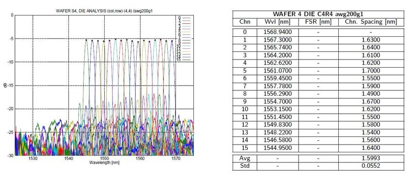
BB Example: 16 Channels AWG @ 200 GHz

                                          Telecom grade specs

                                          Ultracompact design

                                      Also possible in e.g. 1310 nm

9th April, 2012        www.vlcphotonics.com                           19
BB Example: Parametric Echelle gratings
Mux/demux device, optimized for:
- low insertion losses
- low PDL
- low crosstalk
- small size
x high dependence from fabrication
Critical to have the BB
validated for each foundry
Flat surfaces for metallization, or DBR reflectors
9th April, 2012 www.vlcphotonics.com 20BB Example: Asymmetric thermally-tuned MZI
Excellent repeatability even with
design-process decoupling
9th April, 2012 www.vlcphotonics.com 21BB Example: 2x2 MMI (50/50 coupling ratio)
1x2 (50/50)
2x2 (85/15)
2x2 (50/50)
Same device compared in three
different PICs → Excellent repeatability
9th April, 2012 www.vlcphotonics.com 22BB Example: Parametric MMI designs
Symmetric and non-symmetric
coupllng ratios
2×2 MMIs
1×3 MMIs
2×3 MMIs
3×3 MMIs
4×4 MMIs
9th April, 2012 www.vlcphotonics.com 23BB Example: Parametric AWG designs
Telecom Multiplexers / Demultiplexers
Spectrometers
Etc.
All material platforms
Multiple geometries
Custom channel count
and wavelength spacing
9th April, 2012 www.vlcphotonics.com 24Thank you for your attention
info@vlcphotonics.com
www.vlcphotonics.com
@vlcphotonicsYou can also read