ROOM TEMPERATURE IN-SITU MEASUREMENT OF THE SPIN VOLTAGE OF A BISBTE3 THIN FILM
←
→
Page content transcription
If your browser does not render page correctly, please read the page content below
www.nature.com/scientificreports

            OPEN           Room temperature in-situ
                           measurement of the spin voltage of
                           a BiSbTe3 thin film
                           Arthur Leis 1,2,3, Michael Schleenvoigt2,4, Abdur Rehman Jalil 2,4, Vasily Cherepanov 1,2,
                           Gregor Mussler2,4, Detlev Grützmacher2,4, F. Stefan Tautz 1,2,3 & Bert Voigtländer 1,2,3*
                           One of the hallmarks of topological insulators (TIs), the intrinsic spin polarisation in the topologically
                           protected surface states, is investigated at room temperature in-situ by means of four-probe scanning
                           tunnelling microscopy (STM) for a BiSbTe3 thin film. To achieve the required precision of tip positions
                           for measuring a spin signal, a precise positioning method employing STM scans of the local topography
                           with each individual tip is demonstrated. From the transport measurements, the spin polarisation in the
                           topological surface states (TSS) is estimated as p ~ 0.3 – 0.6, which is close to the theoretical limit.

                           Three-dimensional topological insulators (TI) are known to possess topologically protected surface states (TSS)
                           emerging from time-reversal symmetry and strong spin-orbit coupling in the material1–3. Topological surface
                           states are located in the band gap of the TI and form a linearly dispersing Dirac cone. Moreover, these topological
                           surface states are helical in character, so that electrons populating them have a spin that is locked to their momen-
                           tum4. As a consequence of this spin-momentum locking, TI materials in principle allow for the generation of
                           spin-polarised charge carriers merely by the injection of a charge current, without the need of external magnetic
                           fields or ferromagnetic contacts. These and other properties of topological surface states prove to be useful for
                           spintronics5,6 and quantum computation7. It is therefore important to realize TSS with a large degree of helical
                           polarisation, preferably already at room temperature.
                               The helical spin texture of the topological surface states of 3D TIs has been studied extensively by means of
                           angle-resolved photoemission spectroscopy (ARPES)8–12. Recently, also the electrical detection of the intrinsic
                           spin polarisation in TSS has been reported in transport experiments13–21, employing a multi-terminal potentio-
                           metric approach with ferromagnetic (FM) contacts. However, most transport investigations suffer from intrinsic
                           difficulties, such as the parasitic contribution to charge transport through electronic states from the bulk and
                           contaminations introduced during the ex-situ fabrication of devices, which can modify the electronic structure
                           of the TI and the TSS and consequently reduce its spin polarisation. One approach to reduce bulk contributions
                           to transport experiments is reducing the sample thickness either by exfoliation or by growing epitaxial thin film
                           systems. There are clear advantages in using epitaxial thin films, as the Fermi level within the band gap of the
                           compound TI can be tuned by alloying different TI systems such as Bi2Te3 and Sb2Te322–25. Furthermore, epitaxial
                           growth in UHV in conjunction with four-probe STM offers the possibility to measure transport in-situ, i.e. with-
                           out contaminations.
                               In this study, we report the in-situ electrical observation of the intrinsic spin polarisation of charge carriers
                           in a (Bi0.06Sb0.94)2Te3 thin film at room temperature. By using a four-probe STM26, we inject charge carriers from
                           non-magnetic (NM) tungsten tips and measure the spin-dependent voltage drop between a FM nickel tip and
                           a NM tip. From this measurement, we determine the intrinsic spin polarisation in the TSS of the TI thin film to
                           be p ~ 0.3 – 0.6, which is close to theoretical predictions of the maximum value27. The large spin signal in our
                           measurements is attributed to the high quality of the epitaxial films, the in-situ measurement with a four-probe
                           STM, excluding any lithographic processes, and the strong suppression of the contribution of trivial bulk states to
                           charge transport due to thin film conditions, which forces the entirety of the induced charge current through the
                           spin-polarised TSS. We enhance the sensitivity of the measurements by determining the relevant probe distances
                           using STM scans.

                           1
                            Peter Grünberg Institut (PGI-3), Forschungszentrum Jülich, 52425, Jülich, Germany. 2Jülich Aachen Research
                           Alliance (JARA), Fundamentals of Future Information Technology, 52425, Jülich, Germany. 3Experimentalphysik IV
                           A, RWTH Aachen University, Otto-Blumenthal-Straße, 52074, Aachen, Germany. 4Peter Grünberg Institut (PGI-9),
                           Forschungszentrum Jülich, 52425, Jülich, Germany. *email: b.voigtlaender@fz-juelich.de

Scientific Reports |   (2020) 10:2816 | https://doi.org/10.1038/s41598-020-59679-9                                                            1
www.nature.com/scientificreports/ www.nature.com/scientificreports
Figure 1. Measurement principle of the spin-dependent potential with STM tips. (a) Typical transport
measurement setup as seen by the optical microscope. With the four linearly arranged STM tips in contact to
the sample surface acting as electrical probes, a current is induced between the outer two tips, while the
resulting potential difference is measured between the inner ones. (b) Due to the helical→ nature of the TSS, the
orientation of charge carrier spin is perpendicular to their corresponding momentum k and the surface
normal, with the intrinsic TSS spin polarisation p being the degree of helicity. The electrical contact between a
voltage probe and the TI surface can be regarded as two parallel channels with conductances G↑ and G↓ for the
two spin orientations. For a finite probe magnetisation (G↑ ≠ G↓), the voltage probe acquires a spin-dependent
potential Vs, which is given by the interface condition requiring zero current flow (cf. Eq. 1). In this sketch,
charge transport takes place in kx-direction and Δkx denotes the shift of the Fermi circle due to applied bias.
Note that the indicated shift in electrochemical potential v FΔkx cosφ refers to the extremal position φ = 0.
Figure 2. Conceptual sketch of the electrical measurement setup and the resulting potential along the line of
the linearly arranged STM tips. While a NM voltage probe senses the local spin-averaged potential indicated by
the black line (that is logarithmically-shaped in case of a two-dimensional infinite plane31), a magnetised FM tip
acquires the spin-chemical potential Vs. As the spin voltage scales with the current density according to Eq. 2,
the obtained signal is larger if the FM probe is placed close to a current-injecting tip.
Principle of the Spin Voltage Measurement
Using a four-tip STM, four-point resistance measurements on the surface of the TI film are performed in-situ by
positioning the STM tips on the sample and using them as electrical contacts. All measurements are carried out
at room temperature in a UHV environment. Rutherford backscattering spectrometry (RBS) of the TI film com-
position and a previous investigation of a sample grown in the same system28 shows that within the experimental
error, the surface Fermi level EF of our sample is located at the Dirac point (EF = ED = 0).
Due to spin-momentum locking, the spin orientation of charge carriers is directly correlated to their momen-
tum. The injection of a current therefore leads to a net spin polarisation of the current carried by the TSS. The
STM tips are arranged linearly, such that the distance-dependent measurement of the local electrochemical
potential at the surface is enabled, as shown in Figs. 1a and 2. The application of a bias voltage driving the injected
current introduces a shift Δkx of the Fermi circle in the transport direction from its equilibrium position in recip-
rocal space. Because of the linear dispersion relation of the TSS, the electrochemical potential of all states at the
Scientific Reports | (2020) 10:2816 | https://doi.org/10.1038/s41598-020-59679-9 2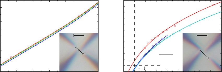
www.nature.com/scientificreports/ www.nature.com/scientificreports
→
original Fermi level is shifted by v FΔkx cosφ, where φ is the angle between the in-plane momentum vector k and
the transport direction (Fig. 1b). Due to the spin-momentum locking (indicated by the arrows in Fig. 1b), a shift
between the average electrochemical potentials of spin-up and spin-down states is introduced, as long as the
intrinsic spin polarisation p is finite. Hence, by applying a bias voltage, the current-induced local electrochemical
potential is spin-split (Fig. 2).
While a non-magnetic contact can only probe the spin-averaged ohmic potential represented by the
black curve in Fig. 2, a FM tip with an effective spin sensitivity PFM = (G↑ − G↓)/(G↑ + G↓)29, given by the
spin-dependent conductances G↑ and G↓ from the FM tip to the sample, can be used to acquire the additional
spin-dependent potential component Vs. Figure 1b illustrates the measurement principle. The electrical contact
between each voltage probe and the TI surface is represented by two parallel channels for the two spin states. At
each point on the TI surface, the voltage probes sit at the potential that is created by the voltage drop between the
injection probes. In case of finite PFM and finite TSS polarisation p, the voltage probe additionally floats to a finite
spin-dependent potential Vs. For an ideal spin probe PFM = 1(−1), Vs is defined as the average electrochemical
potential of charge carriers in the spin-up(-down) state. A general expression for Vs is obtained from the interface
condition requiring zero current flow between the FM voltage probe and the TI surface30
2π v
∫0 dφ[G↑ ↑ ρ ↑ + G↓ ↓ ρ ↓ ]Vs − F Δkx cosφ = 0,
e (1)
where the density operator ρ of the statistical ensemble of charge carriers in the Dirac cone depends on their spin
polarisation p. Hence, ↑ ρ ↑ and ↓ ρ ↓ represent the corresponding probabilities of finding charge carriers in
the spin-up and in the spin-down state, respectively. For ideal spin polarisation p = 1, the probabilities are given
by ↑ ρ ↑ = cos2 φ and ↓ ρ ↓ = sin2 φ . The resulting general expression of the spin potential (as derived in
2 2
Supplementary Note 4) is given by
−1
k T
−E F
h
Vs(x ) = pPFM j(x )kF + B ln1 + e kBT ,
e 2
v
F (2)
with j(x) representing the local current density at the position of the FM probe. Usually, Vs(x) is considered in the
limit EF ≫ kBT20,21,30, resulting in Vs = pPFM h2 1 j(x ), which corresponds to the first term in Eq. 2. In our case, the
e kF
first term is zero, since EF = ED = 0 implies kF = 0. Therefore, the spin voltage is given by the second term of Eq. 2,
as
h v F 1
Vs(x ) = pPFM j(x ),
e 2 kBT ln2 (3)
where the term in brackets originates from the effective wave number of thermally excited charge carriers.
An exemplary tip arrangement as seen in optical microscopy is shown in Fig. 1a. Tips 1 and 4 are tungsten
STM tips placed at fixed positions to inject a charge current I in the TI. Tip 3 is a NM tungsten tip, while tip 2 is a
magnetised FM nickel tip. The latter two are used to probe the local electrochemical potential. To magnetise the
nickel tip in-situ, we use an electromagnet inside the STM chamber. With only one of the two voltage probes being
sensitive to the spin orientation of charge carriers, the measured voltage difference between the two comprises an
ohmic component VΩ and a spin-dependent component Vs, as
I s24 s − D
+ V ,
ΔV = ln − ln 24
2πσ2D s12 s + D s
12 (4)
for purely two-dimensional charge transport31. The corresponding distances are depicted in Fig. 2.
According to Eq. 2, the spin voltage Vs is influenced by material parameters p and vF, the current density
I
( 1
12
)
1
j = 2π s + s at the position of the FM tip31 and its PFM. The spin signal may be obtained in the limit of van-
24
ishing inter-tip distance D → 0, as in this case the first (ohmic) term VΩ in Eq. 4 vanishes. In the experiment, we
keep tips 1, 2, 4 fixed and move tip 3. By measuring the four-point resistance at various D and for opposite FM tip
magnetisation directions, we determine the constant spin contribution and estimate the spin polarisation of the
surface states of the TI.
Results
The electrical measurements are performed on the surface of a 10 nm thin film of (Bi0.06Sb0.94)2Te3 grown by
molecular-beam epitaxy (MBE) on a Si(111) substrate. As the largest spin voltage signal and the highest mobility
is expected for a Fermi level close to the Dirac point, we have chosen the corresponding sample stoichiometry.
After growth, the sample is transferred to the STM chamber by means of a vacuum transfer. The details of the
MBE growth procedure are outlined in a previous publication32. The independent measurement of σ2D which
enters as a parameter in Eq. 4 is presented in Supplementary Note 2.
Spin voltage measurement. For each tip configuration, we infer the corresponding four-point resistance
from IV-characteristics recorded with a maximum induced current of I ≈ 50 μA. In order to determine tip
distances as precisely as possible, we use a method for tip positioning that employs overlapping STM scans. It is
described in more detail below. We use a symmetric configuration with the voltage-probing FM tip positioned
Scientific Reports | (2020) 10:2816 | https://doi.org/10.1038/s41598-020-59679-9 3
www.nature.com/scientificreports/ www.nature.com/scientificreports
Figure 3. Results of the spin voltage measurement in two tip configurations. The spin-sensitive four-point
resistance is measured as function of distance between the inner voltage-probing tips. The tip configuration is
depicted in the insets, respectively. For the sake of comparison between the sets of measurements with slightly
different s12 and s24, the resistance is plotted versus a dimensionless inter-tip distance χ. (a) Measurement
results obtained in the symmetric configuration (s12 ≈ s24 ≈ 3.5 μm). Data points in red and blue correspond to
measurements with opposite magnetisation directions of the FM tip, while data points coloured in green were
obtained with only NM tips, providing a control experiment. (b) In the high current density configuration, the
FM tip is positioned close to a current-injecting tip (s12 ≈ 0.4 μm, s24 ≈ 7 μm). Red and blue/cyan data points
denote resistances acquired with reversed magnetic polarisation directions of the FM tip, respectively. The lines
of corresponding colour represent fits of the resistance model (Eq. 4).
approximately in between the current-inducing tips with s12 ≈ s24 ≈ 3.5 μm. Figure 3a shows results of resistance
measurements corresponding to this tip arrangement. In this figure, the varied inter-tip distance D is replaced by
a normalised dimensionless distance
s12 + s24
χ=D ,
s12s24 (5)
because this allows the direct comparison of results obtained for different distances, as explained in
Supplementary Note 3. Red and blue data points correspond to sets of measurements for which the FM tips have
been magnetised oppositely beforehand. The graph also includes a control measurement with only NM tips rep-
resented by green data points. As can be inferred from the fits of the model function in Eq. 4 to the data sets (lines
of corresponding colour in Fig. 3a), the resistance curves are offset to each other by
ΔV (D → 0) h v F 1 1 1
Rs = = pPFM + ,
I 2
2πe kBT ln2 s12 s24 (6)
resulting from Vs as given by Eq. 3 in the case of a 2D current density. As shown in Fig. 3a, we obtain a finite
resistance offset with inverted signs for opposite magnetisation of the FM tip with Rs = (1.0 ± 0.3) Ω and
Rs = (−1.7 ± 0.2) Ω. In case of our control experiment with an unpolarised tip, we measure a spin resistance
Rs = (0.0 ± 0.1) Ω. When performing the same experiment on a Bi0.53Sb0.47Te3 thin film sample, we do not observe
any offset in the data, which is explained by the large kF in this sample and the correspondingly small Vs (Eq. 2).
The corresponding data are found in Supplementary Note 5. In general, for TI samples of different materials or
doping levels, it is important to keep a low kF and a small bulk carrier contribution in order for the spin voltage
to be pronounced.
While we observe a reversal of the sign of the resistance offset upon changing the FM’s magnetisation direc-
tion, the magnitude of the signal is rather small. The spin-dependent signal can be enhanced using a tip configu-
ration in which the FM probe is situated in a position of high current density, i.e. close (within a few hundred nm)
to a current-injecting tip, resulting in a more pronounced spin-splitting (cf. Fig. 2 and Eq. 3). Figure 3b shows
three sets of resistance measurements with different FM polarisation. As can be seen, finite resistance offsets with
reversed signs are clearly observed at χ = 0 for the respective tip magnetisation orientations. With Rs = (8 ± 2) Ω
for one magnetisation direction and Rs = (−4.8 ± 0.4) Ω and Rs = (−6 ± 2) Ω for the opposite one, the effect is
larger by a factor of ~ 5 compared to the symmetric configuration in Fig. 3a, as expected from the corresponding
increase of the current density.
Tip positioning with STM images. The determination of the spin signal in our transport measurements
is limited by the uncertainty of the four-point resistance arising from the mispositioning of the STM tips on
the surface (see Eq. 6). Since our visual control of the tip positions is based on optical microscopy, the position
uncertainty is given by the latter’s resolution. Even when assuming an optimistic error of ±250 nm, the uncer-
tainty of the ohmic part of the resistance arising from tip positioning controlled by the optical microscope would
amount to δRΩ ≈ 8 Ω (using Eq. 4), which is about the same magnitude as the spin-dependent signal. Since this
uncertainty depends on the local slope of the electrical potential dRΩ/dx ∝ j(x), just as the desired spin signal
Scientific Reports | (2020) 10:2816 | https://doi.org/10.1038/s41598-020-59679-9 4www.nature.com/scientificreports/ www.nature.com/scientificreports
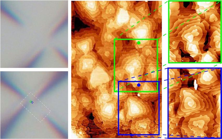
Figure 4. Tip positioning method based on overlapping STM scans used for spin-sensitive transport
measurements. (a) Using one of the STM tips, a large overview scan of the area of the sample surface in which
the contacts will be positioned is acquired. The overview scan (shown partially in (c)) constitutes a map for
further tip navigation. (b,c) Subsequently, all four tips are moved close to their target positions to perform small
scans. Once a topographic structure from the small scan is recognized in the overview scan, the corresponding
tip position within the reference map is known. With all tip positions being identified, the tips can be navigated
to their desired configuration in tunnelling contact by using piezoelectric control. The exact position of each tip
can then be reconfirmed by further scans before contact is finally established.
itself (Eq. 2), this problem cannot be solved by a sophisticated tip arrangement. Therefore, we use a more precise
method of tip positioning to measure the spin-split potential.
Our method of tip positioning employs STM scans of the local sample topography with each of the four tips.
In detail, one of the tips (tip 1) is first used to perform an overview scan of a large area (e.g. 4 μm × 10 μm) of the
sample surface, while the remaining STM tips reside outside of the scanned area (Fig. 4a). Then, the other tips are
moved into the scanned area close to their target positions for the four-probe measurement by use of the optical
microscope. Subsequently, all tips are brought into tunnelling contact and small scans of the sample surface are
performed, as schematically shown in Fig. 4b. By making use of distinct features in the local surface topogra-
phy, these scans can be located in the image of the overview scan (Fig. 4c). After moving all tips to their desired
positions, the STM tips are lowered to the sample surface to establish electrical contact31 and the spin voltage is
measured as described above. For a series of distance-dependent four-point measurements, one of the probes is
retracted into tunnelling contact and moved to the next position. A possible influence of the step edges seen in the
STM scans of the topography on the measured resistance is discussed in Supplementary Note 7.
All inter-tip distances are determined from the tip positions in the large overview scan. As a first approxima-
tion, the inter-tips distances can be accessed by measuring the nominal distances between all tip positions in the
STM overview scan using the calibrated linear piezo constants of the corresponding piezo elements. However, it
is also important to take into account sources of error for the determination of distances in this reference map.
Since time-dependent effects such as creep and thermal drift and the non-linear behaviour of the piezoelectric
effect at high voltages can distort recorded STM images, we consider the impact of these effects on the overview
scan. These effects are evaluated separately, as presented in Supplementary Note 6 and taken into account for the
accurate determination of the tip positions. In total, we estimate that the precision for the determination of the
tip positions is about ±25 nm, i.e. at least an order of magnitude better than in optical microscopy. We find that
the combined uncertainty from tip positioning results in a systematic error of only few percent for the measured
spin resistance Rs.
Discussion
So far, we obtained the spin-dependent resistance offsets Rs (Eq. 6) from the four-point measurements. However,
these values still depend on the specific tip arrangement, while the spin polarisation of the TSS p is the desired
intrinsic quantity. Using the recorded STM scans of the TI surface, the inter-tip distances s12 and s24 can be deter-
mined for each set of measurements. To compare the degree of spin polarisation in our measurements, we define
1 1 h v F 1
S = R s / + = pPFM
s s 2 π e 2 kBT ln2
12 24 (7)
as the critical offset parameter, which only depends on intrinsic material parameters. From the measurements in
Fig. 3a, we identify S = (1.9 ± 0.5) Ωμm and S = (−2.9 ± 0.4) Ωμm for the respective FM magnetisation direc-
tions, while in the case of the measurements in Fig. 3b, S = (3.0 ± 0.8) Ωμm, (−2.9 ± 0.2) Ωμm, (−1.6 ± 0.5) Ω
μm are obtained. According to the model introduced above, the S stemming from the spin-dependent potential
for opposite magnetisations are expected to have the same absolute values but with inverted signs. The observed
variation of the absolute values can be explained by the fact that each set of measurements was performed with
a different (fresh) FM tip and the effective magnetic tip polarisation PFM depends on the microscopic details of
each individual tip.
Scientific Reports | (2020) 10:2816 | https://doi.org/10.1038/s41598-020-59679-9 5www.nature.com/scientificreports/ www.nature.com/scientificreports
To quantify the spin polarisation p in the TSS from our measurements, we make use of the expression for S
(Eq. 7). We use the Fermi velocity vF = 3.8 ⋅ 105 m/s obtained from a previous ARPES measurement of a sample
with the same stoichiometry28 and take into account a geometrical factor of 1/ 2 in PFM due to the 45°-orientation
of the magnetisation direction, which is along the STM tip, with respect to the surface. Hence, a fully polarised
FM tip would yield PFM = 1/ 2 in Eq. 7 in our experimental geometry.
So far, we have only considered the top TSS. Since the current is partially carried by the bottom TSS of the
film, only the fraction of the current that propagates through the top TSS is relevant for determining p. Assuming
that the current divides equally between the top and the bottom TSS and using typical values for the effective spin
polarisation of the ferromagnetic tip33–35 of PFM ~ 0.25–0.5 (without the geometric factor 1/ 2 ), a spin polarisa-
tion in the TSS of p ~ 0.3–0.6 results. This range is similar to values observed in other transport investiga-
tions14,16,18,20,36. The main source of variation of p in our experiment is the value of the tip polarisation.
In the literature, the spin polarisation is sometimes defined as the average spin of all charge carriers with a pos-
itive group velocity in transport direction27,37. Such an averaging over parts of the Fermi circle results in geometric
normalisation factors and hence in maximum spin polarisations below 1. For example, in the definition of Yazyev
et al.27, the integration over half the Fermi circle yields a value of π/4 for the case of ideal spin texture. In contrast,
in our definition of p as the intrinsic spin polarisation of the TSS, the maximum value corresponding to an ideal
helical spin texture is p = 1.
To put our measured value of 0.3–0.6 into perspective, we note that ab initio calculations for TI materials have
shown that the TSS polarisation p as defined in this work can be reduced by ~0.35 due to spin-orbit entangle-
ment27, as the electron spin quantum number is no longer conserved in the corresponding TI systems. Assuming
that there is spin-orbit entanglement in our sample, our measured range of p is remarkably close to the theoretical
limit. Another possible reduction of p results from bulk states. Previous investigations have shown that the coex-
istence of excited bulk states is severely limiting the magnitude of the spin voltage in 3D TIs14,21,29. In this regard,
our thin film system is beneficial as it has been shown that the bulk contribution to the conductivity is negligi-
ble32,38 and that the Te interface layer between our TI film and the substrate does not contribute to the measured
conductivity39.
As suggested in previous publications30,40, spin polarisation signals in transport measurements can also be
interpreted to have other causes such as the bulk Rashba effect or the local Hall effect induced by the stray field
of polarised FM contacts. While the Hall effect can be excluded in our system due to the small dimension of the
contact area of our tips and a general absence of the Hall effect in infinite plane systems41,42, a contribution of the
Rashba effect of bulk states to the spin signal in TI samples is in principle possible29. However, the thermal pop-
ulation of the appropriate spin-split bulk states is expected to be small due to a negligible number of bulk charge
carriers in our thin film system. Furthermore, any contribution of a Rashba effect caused by charge carriers accu-
mulated at the surface of the TI due to band bending43 can be excluded, as the effect of near-surface band bending
is negligible in case of a 10 nm film32,38. The magnitude of our detected signal also seems to be too large to origi-
nate from Rashba-split states, which are expected to contribute less to spin polarisation than the TSS, because of
the smaller Fermi circle and a partial suppression from Rashba states with opposite helicity37. In general, if there
is a bulk Rashba effect concurrent to the TSS, it is expected to be counteracting due to its opposite polarisation37.
In conclusion, we presented spin-sensitive, distance-dependent four-point resistance measurements of the
spin voltage using a four-tip STM. Our tip positioning technique, relying on overlapping scans with each of the
four tips, allows for transport measurements with precisely defined probe geometries. The in-situ spin-sensitive
resistance measurements on the MBE-grown (Bi0.06Sb0.94)2Te3 thin film sample reveal a spin signal at room tem-
perature. With other sources of spin polarisation of charge carriers proven to be irrelevant, we conclude that the
effect is caused by spin-momentum locking in the TSS. A quantitative evaluation, assuming an equal distribution
of the total current between the top and the bottom TSS, leads to an estimate for the TSS spin polarisation of
p ~ 0.3–0.6. This range for the spin polarisation is remarkable, as it is close to the theoretical limit for systems with
spin-orbit entanglement27.
For future applications, BiSbTe3 thin films can be grown on gate-controllable substrates32, enabling the electri-
cal gate control of the spin voltage by changing the Fermi wave number kF of the charge carriers. Furthermore, our
tip positioning method offers possibilities to perform transport measurements on structures that require precise
electrical contacting, such as the edge channels of 2D TI films.
Methods
Sample preparation. The thin-film growth is performed on a 10 × 10 mm2 Si(111) sample by means of
molecular beam epitaxy (MBE). The Si sample is cleaned from organic contaminations and the native oxide
chemically using a wet etching procedure (RCA/hydrofluoric acid). After the transfer to the MBE chamber (base
pressure 1 ⋅ 10−10 mbar) and prior to deposition, the Si sample is heated to 700 °C for 10 min to remove the hydro-
gen termination at the surface that is formed during etching. The subsequent growth of the TI film is carried out
at a substrate temperature of 330 °C and evaporator temperatures of TTe = 325 °C, TBi = 470 °C and TSb = 475 °C,
corresponding to a flux ratio of 100: 10: 1 (Te: Sb: Bi). To ensure the formation of a Te monolayer on the Si(111)
surface at the start of the growth process, the Te evaporator is opened a few seconds ahead of the Bi and Sb evap-
orators. After depositing the thin film and cooling the sample down to room temperature, the sample is loaded
into the four-tip scanning tunnelling microscope (STM) chamber by means of vacuum transfer. Subsequent to the
in-situ measurements, X-ray reflectivity and Rutherford backscattering measurements are performed ex-situ to
confirm the film thickness and to determine the atomic composition of the ternary compound.
Four-probe measurement. The transport investigation is carried out in-situ using a four-tip STM at room
temperature. Electrical contact to the TI film is established by lowering the four STM tips towards the sample
from tunnelling contact. For all measurements, the tips are arranged in a straight line with two tungsten tips
Scientific Reports | (2020) 10:2816 | https://doi.org/10.1038/s41598-020-59679-9 6www.nature.com/scientificreports/ www.nature.com/scientificreports
injecting the current, while the remaining two tips (tungsten and nickel) measure the voltage drop in between.
The distance-dependent four-point resistances are obtained from the resulting IV-characteristics at each respec-
tive tip position. For macroscopic resistance measurements at large tip distances (~50 μm), the tip positioning is
monitored by an optical microscope. In case of resistance measurements at sub-μm distances, the positions of the
tips are controlled using overlapping STM scans performed with each tip. All STM tips used in the experiment
are prepared by electrochemical etching. The ferromagnetic nickel tip is magnetised in-situ in the STM chamber
prior to each set of measurements using an electromagnet.
Data availability
Data within the manuscript and its Supplementary Information is available from the corresponding author upon
reasonable request.
Received: 30 October 2019; Accepted: 3 February 2020;
Published: xx xx xxxx
References
1. Hasan, M. Z. & Kane, C. L. Colloquium: Topological insulators. Rev. Mod. Phys. 82, 3045–3067, https://doi.org/10.1103/
RevModPhys.82.3045 (2010).
2. Qi, X.-L. & Zhang, S.-C. Topological insulators and superconductors. Rev. Mod. Phys. 83, 1057–1110, https://doi.org/10.1103/
RevModPhys.83.1057 (2011).
3. Fu, L., Kane, C. L. & Mele, E. J. Topological insulators in three dimensions. Phys. Rev. Lett. 98, 106803, https://doi.org/10.1103/
PhysRevLett.98.106803 (2007).
4. Moore, J. E. & Balents, L. Topological invariants of time-reversal-invariant band structures. Phys. Rev. B 75, 121306, https://doi.
org/10.1103/PhysRevB.75.121306 (2007).
5. Žutić, I., Fabian, J. & Das Sarma, S. Spintronics: Fundamentals and applications. Rev. Mod. Phys. 76, 323–410, https://doi.
org/10.1103/RevModPhys.76.323 (2004).
6. Pesin, D. & Macdonald, A. Spintronics and pseudospintronics in graphene and topological insulators. Nature Materials 11, 409–416,
https://doi.org/10.1038/nmat3305 (2012).
7. Fu, L. & Kane, C. L. Superconducting proximity effect and majorana fermions at the surface of a topological insulator. Phys. Rev. Lett.
100, 096407, https://doi.org/10.1103/PhysRevLett.100.096407 (2008).
8. Hsieh, D. et al. A tunable topological insulator in the spin helical Dirac transport regime. Nature 460, 1101–5, https://doi.
org/10.1038/nature08234 (2009).
9. Zhang, H. et al. Topological insulators in Bi2Se3, Bi2Te3 and Sb2Te3 with a single Dirac cone on the surface. Nature Physics 5, 438–442,
https://doi.org/10.1038/nphys1270 (2009).
10. Xia, Y. et al. Observation of a large-gap topological-insulator class with a single Dirac cone on the surface. Nature Physics 5, 398–402,
https://doi.org/10.1038/nphys1274 (2009).
11. Pan, Z.-H. et al. Electronic structure of the topological insulator Bi2Se3 using angle-resolved photoemission spectroscopy: Evidence
for a nearly full surface spin polarization. Phys. Rev. Lett. 106, 257004, https://doi.org/10.1103/PhysRevLett.106.257004 (2011).
12. Jozwiak, C. et al. Widespread spin polarization effects in photoemission from topological insulators. Phys. Rev. B 84, 165113, https://
doi.org/10.1103/PhysRevB.84.165113 (2011).
13. Li, H. C. et al. Electrical detection of charge-current-induced spin polarization due to spin-momentum locking in Bi2Se3. Nature
Nanotechnology 9, 218–224, https://doi.org/10.1038/nnano.2014.16 (2014).
14. Dankert, A., Geurs, J., Kamalakar, M. V., Charpentier, S. & Dash, S. P. Room temperature electrical detection of spin polarized
currents in topological insulators. Nano Letters 15, 7976–7981, https://doi.org/10.1021/acs.nanolett.5b03080 (2015).
15. Ando, Y. et al. Electrical detection of the spin polarization due to charge flow in the surface state of the topological insulator Bi1.5 Sb0.5
Te1.7 Se1.3. Nano Letters 14, 6226–6230, https://doi.org/10.1021/nl502546c (2014).
16. Tian, J., Miotkowski, I., Hong, S. & Chen, Y. Electrical injection and detection of spin-polarized currents in topological insulator
Bi2Te2 Se. Scientific Reports 5, 14293, https://doi.org/10.1038/srep14293 (2015).
17. Liu, L. et al. Spin-polarized tunneling study of spin-momentum locking in topological insulators. Phys. Rev. B 91, 235437, https://
doi.org/10.1103/PhysRevB.91.235437 (2015).
18. Lee, J. S., Richardella, A., Hickey, D. R., Mkhoyan, K. A. & Samarth, N. Mapping the chemical potential dependence of current-
induced spin polarization in a topological insulator. Phys. Rev. B 92, 155312, https://doi.org/10.1103/PhysRevB.92.155312 (2015).
19. Tang, J. et al. Electrical detection of spin-polarized surface states conduction in (Bi0.53Sb0.47)2Te3 topological insulator. Nano Letters
14, 5423–5429, https://doi.org/10.1021/nl5026198 (2014).
20. Hus, S. M. et al. Detection of the spin-chemical potential in topological insulators using spin-polarized four-probe STM. Phys. Rev.
Lett. 119, 137202, https://doi.org/10.1103/PhysRevLett.119.137202 (2017).
21. Ko, W. et al. Accessing the intrinsic spin transport in a topological insulator by controlling the crossover of bulk-to-surface
conductance. Phys. Rev. Lett. 121, 176801, https://doi.org/10.1103/PhysRevLett.121.176801 (2018).
22. Kong, D. et al. Ambipolar field effect in the ternary topological insulator (BixSb 1−x) 2Te 3 by composition tuning. Nature
Nanotechnology 6, 705–9, https://doi.org/10.1038/nnano.2011.172 (2011).
23. Zhang, J. et al. Band structure engineering in (Bi1−x Sbx)2 Te3 ternary topological insulators. Nature Communications 2, 574, https://
doi.org/10.1038/ncomms1588 (2011).
24. He, X. et al. Highly tunable electron transport in epitaxial topological insulator (Bi1−xSbx)2 Te3 thin films. Applied Physics Letters 101,
123111, https://doi.org/10.1063/1.4754108 (2012).
25. Weyrich, C. et al. Growth, characterization, and transport properties of ternary (Bi1−xSbx)2Te3. J. Phys.: Condens. Matter 28, 495501,
https://doi.org/10.1088/0953-8984/28/49/495501 (2016).
26. Cherepanov, V. et al. Ultra compact multitip scanning tunneling microscope with a diameter of 50 mm. Review of Scientific
Instruments 83, 033707, https://doi.org/10.1063/1.3694990 (2012).
27. Yazyev, O. V., Moore, J. E. & Louie, S. G. Spin polarization and transport of surface states in the topological insulators Bi2Se3 and
Bi2Te3 from first principles. Phys. Rev. Lett. 105, 266806, https://doi.org/10.1103/PhysRevLett.105.266806 (2010).
28. Kellner, J. et al. Tuning the Dirac point to the Fermi level in the ternary topological insulator (Bi1?xSbx)2Te3. Applied Physics Letters
107, 251603, https://doi.org/10.1063/1.4938394 (2015).
29. Yang, F. et al. Switching of charge-current-induced spin polarization in the topological insulator BiSbTeSe2. Phys. Rev. B 94, 075304,
https://doi.org/10.1103/PhysRevB.94.075304 (2016).
30. Li, P. & Appelbaum, I. Interpreting current-induced spin polarization in topological insulator surface states. Phys. Rev. B 93, 220404,
https://doi.org/10.1103/PhysRevB.93.220404 (2016).
31. Voigtländer, B. et al. Invited Review Article: Multi-tip Scanning Tunneling Microscopy: Experimental Techniques and Data
Analysis. Review of Scientific Instruments 89, 101101, https://doi.org/10.1063/1.5042346 (2018).
Scientific Reports | (2020) 10:2816 | https://doi.org/10.1038/s41598-020-59679-9 7www.nature.com/scientificreports/ www.nature.com/scientificreports
32. Lüpke, F. et al. In situ disentangling surface state transport channels of a topological insulator thin film by gating. npj Quantum
Materials 3, 46, https://doi.org/10.1038/s41535-018-0116-1 (2018).
33. Alvarado, S. F. Tunneling potential barrier dependence of electron spin polarization. Phys. Rev. Lett. 75, 513–516, https://doi.
org/10.1103/PhysRevLett.75.513 (1995).
34. Soulen, R. J. et al. Measuring the spin polarization of a metal with a superconducting point contact. Science 282, 85–88, https://doi.
org/10.1126/science.282.5386.85 (1998).
35. Kim, T. H. & Moodera, J. S. Large spin polarization in epitaxial and polycrystalline Ni films. Phys. Rev. B 69, 020403, https://doi.
org/10.1103/PhysRevB.69.020403 (2004).
36. Dankert, A. et al. Origin and evolution of surface spin current in topological insulators. Phys. Rev. B 97, 125414, https://doi.
org/10.1103/PhysRevB.97.125414 (2018).
37. Hong, S., Diep, V., Datta, S. & Chen, Y. P. Modeling potentiometric measurements in topological insulators including parallel
channels. Phys. Rev. B 86, 085131, https://doi.org/10.1103/PhysRevB.86.085131 (2012).
38. Just, S. et al. 1908.09412v1 .
39. Lüpke, F. et al. Chalcogenide-based van der Waals epitaxy: Interface conductivity of tellurium on Si(111). Phys. Rev. B 96, 035301,
https://doi.org/10.1103/PhysRevB.96.035301 (2017).
40. de Vries, E. K. et al. Towards the understanding of the origin of charge-current-induced spin voltage signals in the topological
insulator Bi2Se3. Phys. Rev. B 92, 201102, https://doi.org/10.1103/PhysRevB.92.201102 (2015).
41. Buehler, M. & Pearson, G. Magnetoconductive correction factors for an isotropic Hall plate with point sources. Solid-State Electronics
9, 395–407, https://doi.org/10.1016/0038-1101(66)90154-7 (1966).
42. Buehler, M. A Hall four-point probe on thin plates: Theory and experiment. Solid-State Electronics 10, 801–812, https://doi.
org/10.1016/0038-1101(67)90163-3 (1967).
43. King, P. D. C. et al. Large tunable Rashba spin splitting of a two-dimensional electron gas in Bi2Se3. Phys. Rev. Lett. 107, 096802,
https://doi.org/10.1103/PhysRevLett.107.096802 (2011).
Acknowledgements
This work was supported by the German excellence cluster ML4Q (Matter and Light for Quantum Computing).
F.S.T. acknowledges support of the Deutsche Forschungsgemeinschaft through the SFB 1083, project A12.
Author contributions
F.S.T., D.G., B.V. and A.L. conceived the research. A.L. performed the transport experiments. A.L., V.C. and B.V.
designed the transport experiments. M.S., A.R.J., G.M. and D.G. carried out the MBE growth of the sample. The
manuscript was written by A.L., B.V. and F.S.T. All authors discussed and commented on the manuscript.
Competing interests
The authors declare no competing interests.
Additional information
Supplementary information is available for this paper at https://doi.org/10.1038/s41598-020-59679-9.
Correspondence and requests for materials should be addressed to B.V.
Reprints and permissions information is available at www.nature.com/reprints.
Publisher’s note Springer Nature remains neutral with regard to jurisdictional claims in published maps and
institutional affiliations.
Open Access This article is licensed under a Creative Commons Attribution 4.0 International
License, which permits use, sharing, adaptation, distribution and reproduction in any medium or
format, as long as you give appropriate credit to the original author(s) and the source, provide a link to the Cre-
ative Commons license, and indicate if changes were made. The images or other third party material in this
article are included in the article’s Creative Commons license, unless indicated otherwise in a credit line to the
material. If material is not included in the article’s Creative Commons license and your intended use is not per-
mitted by statutory regulation or exceeds the permitted use, you will need to obtain permission directly from the
copyright holder. To view a copy of this license, visit http://creativecommons.org/licenses/by/4.0/.
© The Author(s) 2020
Scientific Reports | (2020) 10:2816 | https://doi.org/10.1038/s41598-020-59679-9 8You can also read