SELF-DRIVEN HIGHLY RESPONSIVE PN JUNCTION INSE HETEROSTRUCTURE NEAR-INFRARED LIGHT DETECTOR - ARXIV
←
→
Page content transcription
If your browser does not render page correctly, please read the page content below
Self-Driven Highly Responsive PN Junction
InSe Heterostructure Near-Infrared Light
Detector

CHANDRAMAN PATIL,1,† CHAOBO DONG,1,† HAMED DALIR,1,2
SERGIY KRYLYUK,3 ALBERT V. DAVYDOV,3 AND VOLKER J.
SORGER,1, 2, *
1
 Department of Electrical and Computer Engineering, George Washington University, Washington, DC
20052, USA
2Optelligence   LLC, Upper Marlboro, MD 20772, USA
3Materials   Science and Engineering Division, National Institute of Standards and Technology
Gaithersburg, MD 20899, USA
*sorger@gwu.edu

Abstract: Photodetectors converting light signals into detectable photocurrents are
ubiquitously in use today. To improve the compactness and performance of next-generation
devices and systems, low dimensional materials provide rich physics to engineering the light-
matter interaction. Photodetectors based on two-dimensional (2D) material van der Waals
heterostructures have shown high responsivity and compact integration capability, mainly in
the visible range due to their intrinsic bandgap. The spectral region of near-infrared (NIR) is
technologically important featuring many data communication and sensing applications. While
some initial NIR 2D material-based detectors have emerged, demonstrating doping-junction-
based 2D material photodetectors with the capability to harness the charge-separation
photovoltaic-effect are yet outstanding. Here, we demonstrate a 2D p–n van der Waals
heterojunction photodetector constructed by vertically stacking p-type and n-type few-layer
indium selenide (InSe) 2D flakes. This heterojunction charge-separation-based photodetector
shows a three-fold enhancement in responsivity at near-infrared spectral region (980 nm) as
compared to a photoconductor detector based on p- or n-only doped regions, respectively. We
show, that this junction device exhibits self-powered photodetection operation and hence
enables few pA-low dark currents, which is about 3-4 orders of magnitude more efficient than
state-of-the-art foundry-based devices. Such capability opens doors for small signal-to-noise
environments and low photon-count detectability without having to rely on external gain. We
further demonstrate millisecond response rates in this sensitive zero-bias voltage regime. Such
sensitive photodetection capability in the technologically relevant NIR wavelength region at
low form factors holds promise for several applications including wearable biosensors, 3D
sensing, and remote gas sensing.

Keywords – Indium selenide, heterojunction, 2D pn junction, self-driven photodetector, Near-
infrared detection

1. Introduction

2D semiconducting materials due to their bandgap have been studied as promising
photodetector materials, by changing the layer numbers or forming vdW heterostructures,
owing to their high responsivity, fast response time, broadband photodetection, photo-
detectivity, and low dark current noise [1]-[7]. The operation of these high-performance devices
demands high bias voltage leading to large power consumption due to the Schottky barrier
potential and poor photogenerated carrier collection. This limits technological applications for
remote operation conditions under extreme environments, biomedical sensing, and portable
devices [8]-[11]. However, self-driven photodetectors are promising devices to solve energy
consumption issues where the photon energy is higher than the bandgap of the material for a
better signal-to-noise ratio. Recently, few self-driven 2D material-based photodetectors have
been demonstrated in [9], [12]-[14]. III-VI group 2D materials (InSe, GaSe, and GaTe) have
been recently studied for light-matter interaction properties for optoelectronic applications [15]-
[17]. 2D InSe, with its direct bandgap (~1.25 eV) [18] has recently been investigated showing
higher ultrasensitive photodetection characteristics than other 2D semiconducting materials
such as MoS2 and WSe2 [19]-[22]. For p- and n- doped materials used in heterostructure devices
forms atomically sharp p-n junctions [23]-[25].
   A thorough study has been performed on InSe based photodetectors in the visible spectrum
but is yet to be explored in detail for near-infrared (NIR) applications [26], [27]. Optoelectronic
devices for detection, modulation, and sensing applications in mid infrared spectrum are also
limited by the lack of on-chip sources and high cost of production [28]-[30]. The optoelectronic
devices based on InSe are usually designed in transistor configuration, thus requires high
electrical bias gating or bias voltage [19], [27], [31]. Furthermore, the NIR wavelength at 980
nm is widely used for optical humidity sensing fields such as indoor air quality, industrial
production process control, and agricultural instrumentation [32], [33]. Also, with the
technological advancement in building autonomous vehicles, LiDAR-based devices usually are
designed at 940 – 980 nm wavelengths for short to medium range positioning and mapping
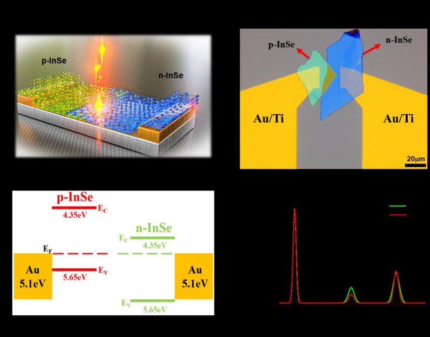
[34], [35]. Due to a direct bandgap (1.25 eV) [18], InSe is an attractive material for
manufacturing optoelectronic devices in this range.
   Here, we demonstrate a self-driven p-InSe/n-InSe heterostructure photodetector for NIR
applications. The p- and n- doped 2D InSe flakes form the vertical heterostructure stack
showing a ~3 times improvement in responsivity and ~3.5 times lower response time as
compared to p- or n-type InSe photodetector thus demonstrating a novel fast and sensitive InSe
heterojunction-based NIR photodetector suitable for low power optical sensors or detector
devices or neuromorphic photonic applications [36], [37].

2. Results and Discussion

Enhancing light-matter interaction by building heterostructures using 2D materials paves a way
towards building high-performance and energy-efficient compact photodetectors [38]. The 2D
material-based photodetectors are often limited by the high bias voltage required for photon-
generated carrier collection due to high resistance and the Schottky barrier [39]. Here, we
demonstrate a pn junction-based photodetector using InSe for near-infrared detection or sensing
applications as seen in Fig. 1a. The 2D InSe flakes are mechanically exfoliated from their bulk
counterpart and transferred precisely on pre-fabricated Au/Ti metal contacts using the novel 2D
material transfer system discussed in [40]. The optical microscope image of the device is shown
in Fig. 1b. The pn InSe heterojunction is formed by using Sn-doped InSe (n-type) and Zn-doped
InSe (p-type) materials grown by a vertical Bridgman method. The band diagram for the device
structure can be seen in Fig. 1c where the in-built heterojunction potential helps in collecting
the photogenerated carriers in the absence of external electrical bias potential. The material
quality was assured after transfer using Raman spectroscopy by observing Raman active modes
for relative intensity peaks at A11g, A21g, and E12g [18].

  The photovoltaic properties of the p-InSe/n-InSe heterojunction, p-InSe, and n-InSe based
photodetector device is studied at 980 nm under vertical illumination using a free-space optical
setup. Fig. 2a shows the current-voltage(I-V) characteristics for photocurrent measurement of
the pn-InSe junction, p-InSe, and n-InSe, where the illumination power is 111.6 μW. The pn-
junction device exhibits an order of magnitude higher photocurrent as compared to the p- and
n- InSe devices. Thus indicating higher photo-absorption at 980 nm for the van der Waals
heterojunction characteristics. Fig. 2b shows the power-dependent photocurrent response of the
pn junction
Fig. 1. PN heterojunction n-InSe/p-InSe photodetector (a) A schematic representation of the n-InSe/p-InSe van der
Waals p-n junction photodetector. (b) An optical micrograph image of the device (top view), where n-InSe was stacked
on the top of the p-InSe flake, transferred on Au/Ti electrodes using the 2D printer technique. (c) Band diagram for p-
InSe (red), n-InSe (green) and Au contact (yellow). (d) The Raman spectra of the p-InSe, n-InSe, and the junction
regions. All material-associated Raman peaks of p-InSe, n-InSe, and pn InSe junction are observed showing peaks
positions and relative intensity associated with out-of-plane vibrational modes (A11g and A21g) and in-plane vibrational
modes (E12g).

device. It can be observed that the photocurrent generation saturates after reaching high optical
incident power intensity. The photovoltaic effect is attributed to the built-in electric field in the
heterojunction depletion region, Fig. 2c shows the dark current mapped at different voltages for
the device. This shows a very small change in the dark current with an increase in the bias
voltage leading to low electrical energy loss. As a result of the built-in potential of the junction,
the device can be operated under no external bias for collecting photo-generated carriers.
Fig. 2d shows the relationship between the photocurrent and the input optical power for pn-
InSe heterojunction, p-InSe, and n-InSe devices under zero bias voltage at 980 nm light
illumination. It can be seen that the built-in potential in the pn junction device shows higher
photocurrent generation as compared to the non-junction (p- and n-) type devices.
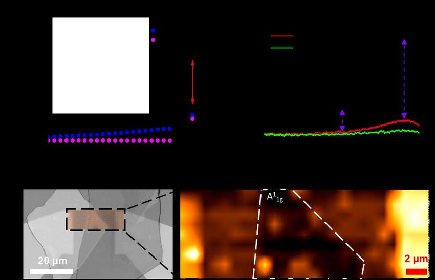
Fig. 2. The photovoltaic characteristics of pn-InSe heterojunction (a) Typical I–V characteristics of p (red), n
(green), and pn junction (black) 2D InSe photodetector. (b) The I-V characteristics of the pn-InSe heterojunction under
different optical input power showing saturation of photocurrent at higher optical power. (c) Dark current mapping
under bias voltage for pn junction device indicates picoamps range current. This exhibits a noise equivalent power
(NEP) of ~2nW/Hz0.5 (*add NEP at 1V*) at zero (1 V) bias. (d) The corresponding fitting curves for the relationship
between the photocurrents and the optical power of the p-InSe/n-InSe heterojunction in zero biased voltage, in 980 nm
light condition.

   Further, the photodetector devices were tested for responsivity as a function of wavelength
from 800 nm to 900 nm (supercontinuum source) and at 980 nm (diode laser) for NIR
photodetection. Fig. 3a shows the responsivity (Rλ=[Iph-Idark]/Pin) of pn heterojunction, p-, and
n- InSe at the zero-bias voltage for pn device and 2 V for p- and n- devices. The pn junction
device shows enhanced responsivity along the NIR wavelength as compared to n- and p-
devices by 3.03 times. It can be found that the maximum responsivity of p-InSe/n-InSe
heterojunction is about 0.5 mAW-1 at 980 nm under zero bias. The photoluminescence (PL)
spectra of the p-InSe, n-InSe, and pn-InSe heterojunction from 800 nm to 1000 nm were
observed using a 532 nm laser for excitation. The peak at 980 nm (1.265 eV) in the PL spectrum
shows the intensity of pn-InSe heterojunction higher than that of p-InSe and n-InSe by ~5.9
times at 980 nm as seen in Fig. 3b. The Raman spectroscopy was used to map the pn junction
stack for observing the clean heterojunction formed between the two flakes. No additional peaks
were observed due to contaminants or defects produced in the material after fabrication [41].

Fig. 3. Spectral characterization of pn-InSe heterojunction (a) Experimental spectra of responsivity of p-InSe, n-
InSe, and pn-InSe heterojunction at 0 V under 800–900 nm and 980 nm light illumination. (b) Photoluminescence
spectra of p-InSe, n-InSe, and p-InSe/n-InSe heterojunction shows strong agreement with the responsivity spectra. An
enhancement of 4.5 times and 5.9 times in intensity is observed at 900 nm and 980 nm, respectively. (c) The quality
of the heterojunction created was assessed at the A11g Raman peak at the physical position of the heterojunction region
(white dashed region), as shown by Raman mapping analysis. A 532 nm laser was used for excitation.

 The photoresponse of the pn-InSe photodetector is expected to be higher than the p- and n-
InSe due to the built-in potential inside the heterojunction. The on/off switching response for
pn-InSe (at 0 V), p- (at -2 V), and n- (at 2 V) photodetector under 980 nm (111.6 μW)
illumination was measured by modulating the optical sources power supply. With an increase
in the external electric field, the charge density in the InSe is high leading to a decrease in
mobility of photo-generated carriers as a result of the decrease in carrier drift velocity. The rise
and fall time of the pn junction device shows a faster response time as compared to the p- and
n-only InSe photodetectors (Fig.4). Due to the absence of junction for p- and n- InSe devices,
the photocarrier collection is possible only after applying an electrical bias. Therefore, both the
devices were tested at 2 V bias for the response time measurement, unlike the built-in electric
field of the p-n junction, light-excited electron-hole pairs can be more effectively separated,
i.e., photovoltaic effect versus relying on a photoconductor for the n- and p-only junction
devices. The response time of pn-InSe device shows a rise time/fall time (τr/τf) response of 8.3
ms/9.6 ms (Fig.4b), which is reduced as compared to n- and p- InSe device by 9.7 ms/30.4 ms
(Fig.4b) and 13.7 ms/19.4 ms (Fig.4c), respectively. This is an interesting result since it shows
the engineerability for designing fast response photodetectors by stacking the 2D materials and
enhancing the optoelectronic properties of the material for various applications.

Fig. 4. Time dependent photoresponse of (a) pn-InSe photodetector at 0 V with rise time/fall time (τr/τf) of 8.3 ms/9.6
ms., (b) n-InSe at 2 V with τr/τf of 18 ms/ 40ms, and (c) p-InSe at -2 V with τr/τf of 22 ms/29 ms . Uunder 980 nm light
illumination.

   Lastly, the pn-junction device was tested for photoresponse and photocurrent mapping at
external bias voltages. The gradient map demonstrates a faster response of the device at zero
bias and also at sub-volt forward bias voltages (Fig. 5a). The nature of the shape of the gradient
is governed by the usually observed pn diode I-V characteristics. The separation of photo-
generated electron-hole pairs is better under the influence of external bias voltage. However,
the device suffers from high charge density leading to lower drift current velocity in the
material. Therefore the time response and sensitivity of the device are adversely affected by
applied external bias. This device shows promising performance for sensing application in the
NIR spectral region owing to its extremely low dark current and response rate at zero external
bias. A summary of the tradeoff between the response time of the device and operational
voltages is represented in Fig. 5b based on the current and previously reported photodetector
devices for NIR applications [42]-[50].
Fig. 5. Photoresponse mapping under external bias (a) Photoresponse at different bias voltage(-2 V to 2 V) with
photocurrent of pn-InSe under 980 nm illumination demonstrated the fastest response under 0 V bias condition. (b)
Comparison of the photoresponse under the external bias of 2D photodetectors for NIR applications discussed in the
literature.

3. Conclusion

A self-driven photodetector was realized for NIR applications at 980 nm and an extremely low
dark current in the range of few picoamps was achieved. The photoresponse of the 2D InSe was
enhanced by building a pn vdW heterojunction using p- and n- doped InSe showing an increase
of ~3 times in responsivity. For comparison, n-InSe and p-Inse photodetector devices were built
as control samples. This tendency was also observed in the PL spectra of the p-, n-, and pn InSe
devices where the intensity was observed to be enhanced by ~6 times in the latter. The device
also demonstrates improvement in response time by ~3.5 times lower than p- or n-type InSe
photodetector. Thus demonstrating a novel fast and sensitive InSe heterojunction-based NIR
photodetector suitable for low power optical sensors or detector devices. Such performance of
this device shows a high potential for realizing a NIR photodetector for sensing and optical
applications. Furthermore, by engineering the interlayer stacking to match closely with the
lattice structure and improving the metal contact Schottky barrier, it is expected that the device
performance in the NIR region will be further improved. Further investigations are required to
determine the chemical and mechanical material stability of the InSe heterojunction structure
under various environmental effects for applications like remote sensing and biological sensing.

4. Methods

4.1 Device Fabrication

              The InSe pn junction heterostructure is formed using 2D flakes exfoliated from its bulk
and transferred using the micro stamp-assisted transfer system on prefabricated electrical
contacts [40]. The electrical contacts were formed using electron beam lithography for a
channel length of 20 µm. The metal Ti/Au (5 nm/45 nm) was deposited using the electron beam
evaporation method. The lift-off was performed using acetone at room temperature followed
by rinsing in isopropyl alcohol and nitrogen drying.
4.2 Device Experimentation
The experimental setup for measuring the 2D InSe pn junction heterostructure devices
comprises a tunable (NKT SUPERCONTINUUM Compact) source and fixed wavelength laser
diode module (CPS980 Thorlbas, INC.) at 980 nm wavelength. The light beam was illuminated
at the junction of the device using an objective lens. A source meter (Keithly 2600B) was used
for electrical response measurements. The response time of the device was measured by
modulating the electrical power supply to the laser. The Raman and photoluminescence
measurements were performed at a laser wavelength of 532 nm.
Disclosures
Data availability. Data underlying the results presented in this paper are not publicly available at this time but may
be obtained from the authors upon reasonable request.
Funding. V.S. is supported by the AFOSR PECASE award (FA9550-20-1-0193).
Acknowledgments. A. V. D. and S. K. acknowledge support through the Material Genome Initiative funding
allocated to NIST.
Disclaimer: Certain commercial equipment, instruments, or materials are identified in this paper in order to specify the
experimental procedure adequately. Such identification is not intended to imply recommendation or endorsement by
the National Institute of Standards and Technology, nor is it intended to imply that the materials or equipment identified
are necessarily the best available for the purpose.
Disclosures. The authors declare no conflict of interaction.
Data availability. Data underlying the results presented in this paper are not publicly available at this time but may
be obtained from the authors upon reasonable request.
†These authors equally contributed to this work.References
1. M. Buscema et al, "Photovoltaic effect in few-layer black phosphorus PN junctions
defined by local electrostatic gating," Nature Communications, vol. 5, (1), pp. 1-
6, 2014.
2. Y. Chen et al, "Two-dimensional WSe2/SnSe pn junctions secure ultrahigh
thermoelectric performance in n-type Pb/I Co-doped polycrystalline SnSe,"
Materials Today Physics, vol. 16, pp. 100306, 2021.
3. S. Kang et al, "2D semiconducting materials for electronic and optoelectronic
applications: potential and challenge," 2D Materials, vol. 7, (2), pp. 022003, 2020.
4. L. Lv et al, "Design and tailoring of two-dimensional Schottky, PN and tunnelling
junctions for electronics and optoelectronics," Nanoscale, vol. 13, (14), pp. 6713-
6751, 2021.
5. R. Maiti et al, "Strain-engineered high-responsivity MoTe 2 photodetector for
silicon photonic integrated circuits," Nature Photonics, vol. 14, (9), pp. 578-584,
2020.
6. X. Yuan et al, "Wafer-scale arrayed pn junctions based on few-layer epitaxial
GaTe," Nano Research, vol. 8, (10), pp. 3332-3341, 2015.
7. T. Zheng et al, "Layer-number dependent and structural defect related optical
properties of InSe," RSC Advances, vol. 7, (87), pp. 54964-54968, 2017.
8. Y. Wang et al, "Applications of 2D-Layered Palladium Diselenide and Its van der
Waals Heterostructures in Electronics and Optoelectronics," Nano-Micro Letters,
vol. 13, (1), pp. 1-52, 2021.
9. X. Zhang et al, "High performance broadband self-driven photodetector based on
MXene (Ti3C2Tx)/GaAs Schottky junction," Mater Des, pp. 109850, 2021.
10. Q. Han et al, "Integrating Near-Infrared Visual Fluorescence with a
Photoelectrochemical Sensing System for Dual Readout Detection of
Biomolecules," Anal. Chem., vol. 93, (7), pp. 3486-3492, 2021.
11. Q. Wu et al, "A simple-structured silicon photodetector possessing asymmetric
Schottky junction for NIR imaging," Physics Letters A, pp. 127586, 2021.
12. H. Shang et al, "A mixed-dimensional 1D Se–2D InSe van der Waals
heterojunction for high responsivity self-powered photodetectors," Nanoscale
Horizons, vol. 5, (3), pp. 564-572, 2020.
13. J. Wu et al, "Enhanced performance of a graphene/GaAs self-driven near-infrared
photodetector with upconversion nanoparticles," Nanoscale, vol. 10, (17), pp.
8023-8030, 2018.
14. Y. Liu et al, "Self-powered and high responsivity photodetector based on a n-Si/p-
GaTe heterojunction," Nanotechnology, vol. 32, (22), pp. 225204, 2021.
15. H. Zhong, Z. Bai and B. Zou, "Tuning the luminescence properties of colloidal I–
III–VI semiconductor nanocrystals for optoelectronics and biotechnology
applications," The Journal of Physical Chemistry Letters, vol. 3, (21), pp. 3167-
3175, 2012.
16. Z. Yang and J. Hao, "Recent progress in 2D layered III–VI semiconductors and
their heterostructures for optoelectronic device applications," Advanced Materials
Technologies, vol. 4, (8), pp. 1900108, 2019.17. C. Ho, "Thickness-dependent carrier transport and optically enhanced
transconductance gain in III-VI multilayer InSe," 2D Materials, vol. 3, (2), pp.
025019, 2016.
18. M. R. Molas et al, "Raman spectroscopy of GaSe and InSe post-transition metal
chalcogenides layers," Faraday Discuss., vol. 227, pp. 163-170, 2021.
19. Z. Chen, J. Biscaras and A. Shukla, "A high performance graphene/few-layer InSe
photo-detector," Nanoscale, vol. 7, (14), pp. 5981-5986, 2015.
20. W. Feng et al, "Ultrahigh photo-responsivity and detectivity in multilayer InSe
nanosheets phototransistors with broadband response," Journal of Materials
Chemistry C, vol. 3, (27), pp. 7022-7028, 2015.
21. O. Lopez-Sanchez et al, "Ultrasensitive photodetectors based on monolayer MoS
2," Nature Nanotechnology, vol. 8, (7), pp. 497-501, 2013.
22. D. A. Nguyen et al, "Highly enhanced photoresponsivity of a monolayer WSe2
photodetector with nitrogen-doped graphene quantum dots," ACS Applied
Materials & Interfaces, vol. 10, (12), pp. 10322-10329, 2018.
23. R. Cheng et al, "Electroluminescence and photocurrent generation from atomically
sharp WSe2/MoS2 heterojunction p–n diodes," Nano Letters, vol. 14, (10), pp.
5590-5597, 2014.
24. S. R. Tamalampudi et al, "High performance and bendable few-layered InSe
photodetectors with broad spectral response," Nano Letters, vol. 14, (5), pp. 2800-
2806, 2014.
25. F. Wang et al, "Tunable GaTe-MoS2 van der Waals p–n junctions with novel
optoelectronic performance," Nano Letters, vol. 15, (11), pp. 7558-7566, 2015.
26. M. Dai et al, "A dual-band multilayer InSe self-powered photodetector with high
performance induced by surface plasmon resonance and asymmetric Schottky
junction," ACS Nano, vol. 12, (8), pp. 8739-8747, 2018.
27. H. Jang et al, "High‐Performance Near‐Infrared Photodetectors Based on Surface‐
Doped InSe," Advanced Functional Materials, vol. 31, (3), pp. 2006788, 2021.
28. E. Heidari et al, "On-chip Fourier transform spectrometer on silicon-on-sapphire,"
Opt. Lett., vol. 44, (11), pp. 2883-2886, 2019.
29. E. Heidari et al, "Hexagonal transverse-coupled-cavity VCSEL redefining the
high-speed lasers," Nanophotonics, vol. 9, (16), pp. 4743-4748, 2020.
30. A. Rostamian et al, "Towards lab-on-chip ultrasensitive ethanol detection using
photonic crystal waveguide operating in the mid-infrared," Nanophotonics, vol.
10, (6), pp. 1675-1682, 2021.
31. L. Liu et al, "Ferroelectric-gated InSe photodetectors with high on/off ratios and
photoresponsivity," Nano Letters, vol. 20, (9), pp. 6666-6673, 2020.
32. H. Li et al, "Optical humidity sensor based on ZnO nanomaterials," in 2020 IEEE
5th Optoelectronics Global Conference (OGC), 2020, .
33. S. Sikarwar et al, "Fabrication of nanostructured yttria stabilized zirconia
multilayered films and their optical humidity sensing capabilities based on
transmission," Sensors Actuators B: Chem., vol. 232, pp. 283-291, 2016.
34. H. J. Lee, K. Y. Jung and Y. Kim, "Nanostructured Fe 2 O 3/TiO 2 composite
particles with enhanced NIR reflectance for application to LiDAR detectable cool
pigments," RSC Advances, vol. 11, (28), pp. 16834-16840, 2021.35. A. Jha, "A review of visible, near-IR, and mid-IR transitions in rare-earth doped
glass waveguides for remote sensing and LIDAR," in Lidar Remote Sensing for
Environmental Monitoring VII, 2006, .
36. R. Amin et al, "ITO-based electro-absorption modulator for photonic neural
activation function," APL Materials, vol. 7, (8), pp. 081112, 2019.
37. J. K. George et al, "Neuromorphic photonics with electro-absorption modulators,"
Optics Express, vol. 27, (4), pp. 5181-5191, 2019.
38. R. Maiti et al, "Loss and coupling tuning via heterogeneous integration of MoS 2
layers in silicon photonics," Optical Materials Express, vol. 9, (2), pp. 751-759,
2019.
39. C. Patil, R. Maiti and V. J. Sorger, "WS2 monolayer integrated photodetector," in
CLEO: QELS_Fundamental Science, 2020, .
40. R. A. Hemnani et al, "2D material printer: a deterministic cross contamination-free
transfer method for atomically layered materials," 2D Mater., vol. 6, (1), pp.
015006, 2018. Available: https://doi.org/10.1088/2053-1583/aae62a. DOI:
10.1088/2053-1583/aae62a.
41. S. Gupta, E. Heintzman and J. Jasinski, "Multiphonon Raman spectroscopy
properties and Raman mapping of 2D van der Waals solids: graphene and beyond,"
J. Raman Spectrosc., vol. 46, (2), pp. 217-230, 2015.
42. S. Zhao et al, "Highly Polarized and Fast Photoresponse of Black Phosphorus‐InSe
Vertical p–n Heterojunctions," Advanced Functional Materials, vol. 28, (34), pp.
1802011, 2018.
43. L. Ye et al, "Near-infrared photodetector based on MoS2/black phosphorus
heterojunction," Acs Photonics, vol. 3, (4), pp. 692-699, 2016.
44. F. Wang et al, "Submillimeter 2D Bi2Se3 Flakes toward High‐Performance
Infrared Photodetection at Optical Communication Wavelength," Advanced
Functional Materials, vol. 28, (33), pp. 1802707, 2018.
45. D. Kufer et al, "Hybrid 2D–0D MoS2–PbS quantum dot photodetectors," Adv
Mater, vol. 27, (1), pp. 176-180, 2015.
46. H. J. Jin et al, "Ultrasensitive WSe2/α-In2Se3 NIR Photodetector Based on
Ferroelectric Gating Effect," Advanced Materials Technologies, vol. n/a, (n/a), pp.
2100494, Available:
https://onlinelibrary.wiley.com/doi/abs/10.1002/admt.202100494. DOI:
10.1002/admt.202100494.
47. M. Hafeez et al, "Chemical vapor deposition synthesis of ultrathin hexagonal
ReSe2 flakes for anisotropic raman property and optoelectronic application," Adv
Mater, vol. 28, (37), pp. 8296-8301, 2016.
48. H. Fu et al, "Different-sized black phosphorus nanosheets with good
cytocompatibility and high photothermal performance," RSC Advances, vol. 7,
(24), pp. 14618-14624, 2017.
49. W. Feng et al, "Ultrahigh photo-responsivity and detectivity in multilayer InSe
nanosheets phototransistors with broadband response," Journal of Materials
Chemistry C, vol. 3, (27), pp. 7022-7028, 2015.
50. B. Chitara et al, "Ultrathin Bi 2 O 2 S nanosheet near-infrared photodetectors,"
Nanoscale, vol. 12, (30), pp. 16285-16291, 2020.You can also read