SI5330X DATA SHEET - SKYWORKS
←
→
Page content transcription
If your browser does not render page correctly, please read the page content below

Si5330x Data Sheet

Ultra-Low Additive Jitter Fanout Clock Buffers with up to 10
                                                                                                 KEY FEATURES
Universal Outputs from Any-Format Input and Wide Frequency
Range from 1 MHz to 725 MHz                                                                       • Ultra-low additive jitter: 50 fs rms
                                                                                                  • Built-in LDOs for high PSRR performance
The Si5330x family of Universal/Any-format fanout buffers is ideal for clock distribution
(1 MHz minimum) and redundant clocking applications. These devices feature typical                • Up to 10 outputs
ultra-low jitter characteristics of 50 fs and operate over a wide frequency range. Built-in       • Any-format Inputs (LVPECL, Low-power
LDOs deliver high PSRR performance and reduce the need for external components,                     LVPECL, LVDS, CML, HCSL, LVCMOS)
simplifying low-jitter clock distribution in noisy environments.                                  • Wide frequency range
                                                                                                  • Output Enable option
The Si5330x family is available in multiple configurations, with some versions offering
                                                                                                  • Multiple configuration options
a selectable input clock using a 2:1 input mux. Other features include independent
                                                                                                    • Dual Bank option
(synchronous) output enable, glitchless switching, LOS monitor of input clocks, output
clock division, and built-in format translation. These buffers can be paired with the               • 2:1 Input Mux operation
Si534x clocks and jitter attenuators, the Si5332 clocks, and the Si5xx oscillators to             • Synchronous output enable
deliver end-to-end clock tree performance.                                                        • Loss of signal (LOS) monitors for loss of
                                                                                                    input clock
                                                                                                  • Output clock division: /1, /2, /4
                                                                                                  • RoHS compliant, Pb-free
                                                                                                  • Temperature range: –40 to +85 °C

             Skyworks Solutions, Inc. • Phone [781] 376-3000 • Fax [781] 376-3100 • sales@skyworksinc.com • www.skyworksinc.com
1    Rev. 1.0 • Skyworks Proprietary Information • Products and Product Information are Subject to Change Without Notice • November 5, 2021     1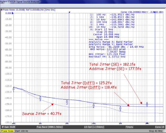
Si5330x Data Sheet • Ordering Guide

1. Ordering Guide

                                                     Table 1.1. Product Family Overview

       Part                 Description            Input    Input      Output         Glitch-      LOS       OE         Synchro-      Clk Divid-
      Number                                       MUX                                 less       Output    Option      nous OE1      er Option
                                                                                      Switch1

    Si53301-B-GM     6 output universal buffer      Yes       2       6 Diff / 12       Yes        Yes     Per Bank         Yes        Per Bank
                        with 2:1 input mux                               SE

    Si53302-B-GM     10 output universal buffer     Yes       2      10 Diff / 20       Yes        Yes     Per Bank         Yes        Per Bank
                        with 2:1 input mux                              SE

    Si53303-B-GM     Dual 1:5 universal buffer      No        2       5 Diff / 10        No        No      Per Bank         Yes        Per Bank
                                                                         SE

    Si53304-B-GM     6 output universal buffer      Yes       2       6 Diff / 12       Yes        No      Individual       Yes            No
                        with 2:1 input mux                               SE

    Si53305-B-GM     10 output universal buffer     Yes       2      10 Diff / 20       Yes        No      Individual       Yes            No
                        with 2:1 input mux                              SE

    Si53306-B-GM     4 output universal buffer,     No        1      4 Diff / 8 SE       No        No       Single          Yes            No
                           single input

    Si53307-B-GM     2 output universal buffer      Yes       2      2 Diff / 4 SE      Yes        No       Single          Yes            No
                        with 2:1 input mux

    Si53308-B-GM     Dual 1:3 universal buffer      No        2      3 Diff / 6 SE       No        Yes     Per Bank         Yes        Per Bank

Note:
 1. The synchronous features (Glitch-less switching and Synchronous OE) of the Si533xx family require a minimum input clock
    frequency of 1 MHz. If the selected input clock stops, pauses, or is gapped such that the 1 MHz minimum is not met for any
    time interval, then the output clock(s) will be disabled (turned off). Once the paused input clock restarts, the output clock may
    NOT start up immediately. Output start-up (turning back on) may be delayed for several input clock cycles until the internal
    synchronizer determines the input clock is once again valid.
 2. Click on the part number above to see a block diagram for each corresponding part number.

                                                     Table 1.2. Si5330x Ordering Guide

           Part Number                            Package                            Pb-Free, ROHS-6                      Temperature

         Si53301-B-GM1                             32-QFN                                 Yes                             –40 to 85 °C

         Si53302-B-GM1                             44-QFN                                 Yes                             –40 to 85 °C

         Si53303-B-GM1                             44-QFN                                 Yes                             –40 to 85 °C

         Si53304-B-GM1                             32-QFN                                 Yes                             –40 to 85 °C

         Si53305-B-GM1                             44-QFN                                 Yes                             –40 to 85 °C

         Si53306-B-GM1                             16-QFN                                 Yes                             –40 to 85 °C

         Si53307-B-GM1                             16-QFN                                 Yes                             –40 to 85 °C

         Si53308-B-GM1                             32-QFN                                 Yes                             –40 to 85 °C

          Si53301/4-EVB                       Evaluation Board                                —                                 —

Note:
 1. Add an "R" at the end of the OPN to denote tape and reel ordering options.

               Skyworks Solutions, Inc. • Phone [781] 376-3000 • Fax [781] 376-3100 • sales@skyworksinc.com • www.skyworksinc.com
2      Rev. 1.0 • Skyworks Proprietary Information • Products and Product Information are Subject to Change Without Notice • November 5, 2021      2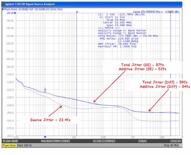
Table of Contents
1. Ordering Guide             . . . . . . . . . . . . . . . . . . . . . . . . . . . . . . 2
2. Functional Description. . . . . . . . . . . . . . . . . . . . . . . . . . . . 5
    2.1 Universal, Any-Format Input Termination .                    .   .   .   .   .   .   .   .   .   .   .   .   .   .   .   .   .   .   .   . 5
    2.2 Internal Input Bias Resistors            .   .   .   .   .   .   .   .   .   .   .   .   .   .   .   .   .   .   .   .   .   .   .   .   . 8
    2.3 Voltage Reference (VREF) .               .   .   .   .   .   .   .   .   .   .   .   .   .   .   .   .   .   .   .   .   .   .   .   .   . 9
    2.4 Universal, Any-Format Output Buffer                  .   .   .   .   .   .   .   .   .   .   .   .   .   .   .   .   .   .   .   .   .   . 9
    2.5 Input Mux (Si53301/02/04/05/07 Only) .                   .   .   .   .   .   .   .   .   .   .   .   .   .   .   .   .   .   .   .   .   .10
    2.6 Glitchless Clock Input Switching .               .   .   .   .   .   .   .   .   .   .   .   .   .   .   .   .   .   .   .   .   .   .   .10
    2.7 Synchronous Output Enable                .   .   .   .   .   .   .   .   .   .   .   .   .   .   .   .   .   .   .   .   .   .   .   .   .10
    2.8 Loss of Signal (LOS) Indicator .             .   .   .   .   .   .   .   .   .   .   .   .   .   .   .   .   .   .   .   .   .   .   .   .11
    2.9 Flexible Output Divider .            .   .   .   .   .   .   .   .   .   .   .   .   .   .   .   .   .   .   .   .   .   .   .   .   .   .11
    2.10 Power Supply (VDD and VDDOX) .                  .   .   .   .   .   .   .   .   .   .   .   .   .   .   .   .   .   .   .   .   .   .   .11
    2.11 Output Clock Termination Options .                  .   .   .   .   .   .   .   .   .   .   .   .   .   .   .   .   .   .   .   .   .   .12
    2.12 LVCMOS Output Termination to Support 1.5 V and 1.2 V .                              .   .   .   .   .   .   .   .   .   .   .   .   .   .14
    2.13 AC Timing Waveforms .               .   .   .   .   .   .   .   .   .   .   .   .   .   .   .   .   .   .   .   .   .   .   .   .   .   .15
    2.14 Typical Phase Noise Performance (Differential Input Clock)                          .   .   .   .   .   .   .   .   .   .   .   .   .   .16
    2.15 Typical Phase Noise Performance (Single-Ended Input Clock)                              .   .   .   .   .   .   .   .   .   .   .   .   .18
    2.16 Input Mux Noise Isolation .             .   .   .   .   .   .   .   .   .   .   .   .   .   .   .   .   .   .   .   .   .   .   .   .   .19
    2.17 Power Supply Noise Rejection .                  .   .   .   .   .   .   .   .   .   .   .   .   .   .   .   .   .   .   .   .   .   .   .19

3. Electrical Specifications . . . . . . . . . . . . . . . . . . . . . . . . . .                                                                 20
4. Detailed Block Diagrams . . . . . . . . . . . . . . . . . . . . . . . . . .                                                                   29
5. Pin Descriptions . . . . . . . . . . . . . . . . . . . . . . . . . . . . .                                                                    36
    5.1 Si53301 Pin Descriptions             .   .   .   .   .   .   .   .   .   .   .   .   .   .   .   .   .   .   .   .   .   .   .   .   .   .36
    5.2 Si53302 Pin Descriptions             .   .   .   .   .   .   .   .   .   .   .   .   .   .   .   .   .   .   .   .   .   .   .   .   .   .39
    5.3 Si53303 Pin Descriptions             .   .   .   .   .   .   .   .   .   .   .   .   .   .   .   .   .   .   .   .   .   .   .   .   .   .42
    5.4 Si53304 Pin Descriptions             .   .   .   .   .   .   .   .   .   .   .   .   .   .   .   .   .   .   .   .   .   .   .   .   .   .45
    5.5 Si53305 Pin Descriptions             .   .   .   .   .   .   .   .   .   .   .   .   .   .   .   .   .   .   .   .   .   .   .   .   .   .48
    5.6 Si53306 Pin Descriptions             .   .   .   .   .   .   .   .   .   .   .   .   .   .   .   .   .   .   .   .   .   .   .   .   .   .52
    5.7 Si53307 Pin Descriptions             .   .   .   .   .   .   .   .   .   .   .   .   .   .   .   .   .   .   .   .   .   .   .   .   .   .54
    5.8 Si53308 Pin Descriptions             .   .   .   .   .   .   .   .   .   .   .   .   .   .   .   .   .   .   .   .   .   .   .   .   .   .56

6. Package Outlines . . . . . . . . . . . . . . . . . . . . . . . . . . . . .                                                                    59
    6.1 16-QFN Package Diagram .                 .   .   .   .   .   .   .   .   .   .   .   .   .   .   .   .   .   .   .   .   .   .   .   .   .59
    6.2 32-QFN Package Diagram .                 .   .   .   .   .   .   .   .   .   .   .   .   .   .   .   .   .   .   .   .   .   .   .   .   .60
    6.3 44-QFN Package Diagram .                 .   .   .   .   .   .   .   .   .   .   .   .   .   .   .   .   .   .   .   .   .   .   .   .   .61

7. Land Patterns . . . . . . . . . . . . . . . . . . . . . . . . . . . . . .                                                                     62
              Skyworks Solutions, Inc. • Phone [781] 376-3000 • Fax [781] 376-3100 • sales@skyworksinc.com • www.skyworksinc.com
3     Rev. 1.0 • Skyworks Proprietary Information • Products and Product Information are Subject to Change Without Notice • November 5, 2021       3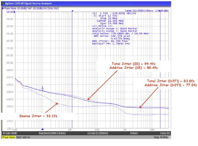
7.1 16-QFN Land Pattern.             .   .   .   .   .   .   .   .   .   .   .   .   .   .   .   .   .   .   .   .   .   .   .   .   .   .   .62
    7.2 32-QFN Land Pattern.             .   .   .   .   .   .   .   .   .   .   .   .   .   .   .   .   .   .   .   .   .   .   .   .   .   .   .63
    7.3 44-QFN Land Pattern.             .   .   .   .   .   .   .   .   .   .   .   .   .   .   .   .   .   .   .   .   .   .   .   .   .   .   .64

8. Top Markings . . . . . . . . . . . . . . . . . . . . . . . . . . . . . .                                                                      65
    8.1 Si53301/04/08 Top Markings .                 .   .   .   .   .   .   .   .   .   .   .   .   .   .   .   .   .   .   .   .   .   .   .   .65
    8.2 Si53302/03/05 Top Markings .                 .   .   .   .   .   .   .   .   .   .   .   .   .   .   .   .   .   .   .   .   .   .   .   .66
    8.3 Si53306/07 Top Markings .                .   .   .   .   .   .   .   .   .   .   .   .   .   .   .   .   .   .   .   .   .   .   .   .   .67

9. Revision History . . . . . . . . . . . . . . . . . . . . . . . . . . . . .                                                                    68

              Skyworks Solutions, Inc. • Phone [781] 376-3000 • Fax [781] 376-3100 • sales@skyworksinc.com • www.skyworksinc.com
4     Rev. 1.0 • Skyworks Proprietary Information • Products and Product Information are Subject to Change Without Notice • November 5, 2021       4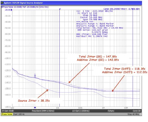
Si5330x Data Sheet • Functional Description

2. Functional Description

The Si5330x family of low-jitter, low-skew, universal/any-format buffers accepts most common differential or LVCMOS input signals.
These devices are available in multiple configurations customized for the end application (refer to 1. Ordering Guide for more details on
configurations).

2.1 Universal, Any-Format Input Termination

The universal input stage enables simple interfacing to a wide variety of clock formats, including LVPECL, low-power LVPECL,
LVCMOS, LVDS, HCSL, and CML. The simplified tables below summarize the various ac- and dc-coupling options supported by the
device. For the best high-speed performance, the use of differential formats is recommended. For both single-ended and differential
input clocks, the fastest possible slew rate is recommended since low slew rates can increase the noise floor and degrade jitter
performance. Though not required, a minimum slew rate of 0.75 V/ns is recommended for differential formats and 1.0 V/ns for
single-ended formats. See AN766: Understanding and Optimizing Clock Buffer’s Additive Jitter Performance for more information.

                                               Table 2.1. AC-Coupled Clock Input Options

                            Clock Format                                                1.8 V                              2.5/3.3 V

                    LVPECL/Low-power LVPECL                                              N/A                                  Yes

                               LVCMOS                                                    No                                   Yes

                                 LVDS                                                    Yes                                  Yes

                                 HCSL                                                    No                                   Yes

                                  CML                                                    Yes                                  Yes

                                               Table 2.2. DC-Coupled Clock Input Options

                            Clock Format                                                1.8 V                              2.5/3.3 V

                    LVPECL/Low-power LVPECL                                              N/A                                  Yes

                               LVCMOS                                                    No                                   Yes

                                 LVDS                                                    No                                   Yes

                                 HCSL                                                    No                                   Yes

                                  CML                                                    No                                   No

              Skyworks Solutions, Inc. • Phone [781] 376-3000 • Fax [781] 376-3100 • sales@skyworksinc.com • www.skyworksinc.com
5     Rev. 1.0 • Skyworks Proprietary Information • Products and Product Information are Subject to Change Without Notice • November 5, 2021   5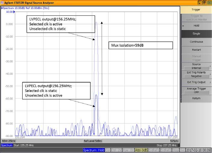
Si5330x Data Sheet • Functional Description

                                                                                                        VDD

                                               0.1 µF                                               Si5330x
                                                                                 CLKx

                                                        100
                                                                                CLKxb

                                               0.1 µF
             Figure 2.1. Differential (HCSL, LVPECL, Low-Power LVPECL, LVDS, CML) AC-Coupled Input Termination

                                                                                                          VDD

                                                                                                                                         VDD
                                                                                                   1k
       VDD = 3.3 V or 2.5 V
                                                                                                                                        Si5330x
    CMOS                                                                                                              CLKx
                                                           50
    Driver
                              Rs                                                                                      CLKxb

                                                                             VTERM = VDD/2
    Note:                                                                                          1k
    Value for Rs should be chosen so that the total
    source impedance matches the characteristic
    impedance of the PCB trace.

                                    Figure 2.2. DC-Coupled, Single-Ended (LVCMOS) Input Termination

                                                                                             VDD
                                                                                                    VDD
                                                                                        1k
                                                                                                                                VDD
                                                                                                          1k
                   VDD = 3.3 V or 2.5 V                              VBIAS = VDD/2
                                                                                                                              Si5330x
                 CMOS                                                                                          CLKx
                                                                50
                 Driver
                                          Rs                                                               CLKxb

                                                                                        1k
                                                                                                          1k
                Notes:
                1. Assumes all VDDs are at the same level.
                                                                                                                        VTERM = VDD/2
                2. Value for Rs should be chosen so that the total
                   source impedance matches the characteristic
                   impedance of the PCB trace.

                                    Figure 2.3. AC-Coupled, Single-Ended (LVCMOS) Input Termination

              Skyworks Solutions, Inc. • Phone [781] 376-3000 • Fax [781] 376-3100 • sales@skyworksinc.com • www.skyworksinc.com
6     Rev. 1.0 • Skyworks Proprietary Information • Products and Product Information are Subject to Change Without Notice • November 5, 2021      6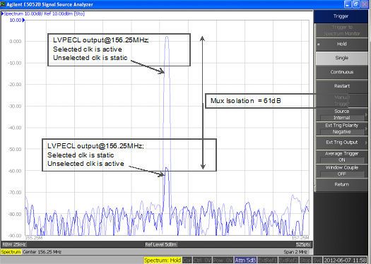
Si5330x Data Sheet • Functional Description

                                                                                                  VDD

                 DC Coupled LVPECL Input Termination Scheme 1
                                                                                                                     VDD
                                                                                        R1              R1
                             VDD = 3.3 V or 2.5 V
                                                                                                                           Si5330x
                    “Standard”                                 50                                        CLKx
                     LVPECL
                                                                                                         CLKxb
                      Driver
                                                               50

                                                                                        R2              R2      VTERM = VDD – 2V
                                                                                                                R1 // R2 = 50 Ohm
                             3.3 V LVPECL: R1 = 127 Ohm, R2 = 82.5 Ohm
                             2.5 V LVPECL: R1 = 250 Ohm, R2 = 62.5 Ohm

                 DC Coupled LVPECL Input Termination Scheme 2
                                                                              VTERM = VDD – 2 V

                                                                                                                     VDD
                                                                            50               50
                            VDD = 3.3 V or 2.5 V
                                                                                                                           Si5330x
                    “Standard”                                 50                                        CLKx
                     LVPECL
                                                                                                         CLKxb
                      Driver
                                                               50

                 DC Coupled LVDS Input Termination                                                                   VDD

                            VDD = 3.3 V or 2.5 V
                                                                                                                           Si5330x
                    Standard                                   50                                            CLKx
                     LVDS                                                         100                    CLKxb
                     Driver
                                                               50

                  DC Coupled HCSL Input Termination                                                                  VDD

                            VDD = 3.3 V or 2.5 V
                                                    33                                                                     Si5330x
                                                                                 50                          CLKx
                    Standard
                   HCSL Driver                      33                                                   CLKxb
                                                                                 50

                                                         50            50

                                 Note: 33 Ohm series termination is optional depending on the location of the receiver.

                                           Figure 2.4. Differential DC-Coupled Input Terminations

              Skyworks Solutions, Inc. • Phone [781] 376-3000 • Fax [781] 376-3100 • sales@skyworksinc.com • www.skyworksinc.com
7     Rev. 1.0 • Skyworks Proprietary Information • Products and Product Information are Subject to Change Without Notice • November 5, 2021   7
Si5330x Data Sheet • Functional Description
Table 2.3. AC/DC-Coupled Clock Input Requirements for Glitchless, Non-Continuous Clocks1, 2, 3
Input Clock Driver Stop State
Clock Input Type
Low High High-Z
DC-Coupled Yes Yes No
AC-Coupled Yes No No
Note:
1. "Non-continuous clocks” means any clock that can be stopped, disabled, or gapped.
2. “Yes” means this configuration is supported.
3. “No” indicates that the configuration is not supported. Operating under a "No" condition can result in erroneous clock outputs
and/or erroneous LOS indications. Operating the device in unsupported configurations is not recommended.
2.2 Internal Input Bias Resistors
Internal bias resistors ensure a differential output low condition in the event that the clock inputs are not connected. The clock input
should not be actively driven when power is not applied to the device. The non-inverting input is biased with a 18.75 kΩ pull-down to
GND and a 75 kΩ pull-up to VDD. The inverting input is biased with a 75 kΩ pull-up to VDD.
VDD
Si5330x
RPU RPU
+
CLK0 or RPD
CLK1
–
RPU = 75 k
RPD = 18.75 k
Figure 2.5. Internal Input Bias Resistors
Skyworks Solutions, Inc. • Phone [781] 376-3000 • Fax [781] 376-3100 • sales@skyworksinc.com • www.skyworksinc.com
8 Rev. 1.0 • Skyworks Proprietary Information • Products and Product Information are Subject to Change Without Notice • November 5, 2021 8Si5330x Data Sheet • Functional Description
2.3 Voltage Reference (VREF)
The VREF pin can be used to bias the input receiver, as shown in the figure below, when a single-ended input clock (such as LVCMOS)
is used. Note that VREF = VDD/2 and should be compatible with the Vcm rating of the single-ended input clock driving the CLK0 or
CLK1 inputs. To optimize jitter and duty cycle performance, use the circuit in Figure 2.3 AC-Coupled, Single-Ended (LVCMOS) Input
Termination on page 6. VREF pin should be left floating when differential clocks are used.
VDDO = 3.3V , 2.5V
Si5330x
Rs
CMOS Driver CLKx
50
CLKxb
VREF
100 nF
Figure 2.6. Using Voltage Reference with Single-Ended Input Clock
2.4 Universal, Any-Format Output Buffer
The highly flexible output drivers support a wide range of clock signal formats, including LVPECL, low power LVPECL, LVDS, CML,
HCSL, and LVCMOS. SFOUTx[1] and SFOUTx[0] are 3-level inputs that can be pinstrapped to select the Bank A and Bank B clock
signal formats independently. This feature enables the device to be used for format/level translation in addition to clock distribution,
minimizing the number of unique buffer part numbers required in a typical application and simplifying design reuse. For EMI reduction
applications, four LVCMOS drive strength options are available for each VDDO setting.
Table 2.4. Output Signal Format Selection
SFOUTx[1] SFOUTx[0] VDDOX = 3.3 V VDDOX = 2.5 V VDDOX = 1.8 V
Open1 Open1 LVPECL LVPECL N/A
0 0 LVDS LVDS LVDS
0 1 LVCMOS, 24 mA drive LVCMOS, 18 mA drive LVCMOS, 12 mA drive
1 0 LVCMOS, 18 mA drive LVCMOS, 12 mA drive LVCMOS, 9 mA drive
1 1 LVCMOS, 12 mA drive LVCMOS, 9 mA drive LVCMOS, 6 mA drive
Open1 0 LVCMOS, 6 mA drive LVCMOS, 4 mA drive LVCMOS, 2 mA drive
Open1 1 LVPECL Low power LVPECL Low power N/A
0 Open1 CML CML CML
1 Open1 HCSL HCSL N/A
Note:
1. SFOUTx[1:0] are 3-level input pins. Tie low for “0” setting. Tie high for “1” setting. When left open, the pin is internally biased to
VDD/2.
Skyworks Solutions, Inc. • Phone [781] 376-3000 • Fax [781] 376-3100 • sales@skyworksinc.com • www.skyworksinc.com
9 Rev. 1.0 • Skyworks Proprietary Information • Products and Product Information are Subject to Change Without Notice • November 5, 2021 9Si5330x Data Sheet • Functional Description
2.5 Input Mux (Si53301/02/04/05/07 Only)
The Si53301/02/04/05/07 provide two clock inputs for applications that need to select between one of two clock sources. The CLK_SEL
pin selects the active clock input and has an internal pulldown resistor. The following table summarizes the input and output clock
based on the input mux pin settings.
Table 2.5. Input Mux Logic
CLK_SEL CLK0 CLK1 Q1 Qb
L L X L H
L H X H L
H X L L H
H X H H L
Note:
1. On the next negative transition of CLK0 or CLK1.
2.6 Glitchless Clock Input Switching
The Si53301/2/4/5/7 feature glitchless switching between two valid input clocks. The following figure illustrates that switching between
input clocks does not generate runt pulses or glitches at the output.
CLK1
CLK0
CLK_SEL
Note 1 Note 2 Note 3
Qn
Notes:
1. Qn continues with CLK0 for 2-3 falling edges of CLK0.
2. Qn is disabled low for 2-3 falling edges of CLK1 .
3. Qn starts on the first rising edge after 1 + 2.
Figure 2.7. Glitchless Input Clock Switch
The Si53301/2/4/5/7 support glitchless switching between clock inputs with a frequency variance up to 10x. When a switchover to a
new clock is made, the output will disable low after two or three clock cycles of the previously selected input clock. The outputs will
remain low for up to three clock cycles of the newly-selected clock, after which the outputs will start from the newly-selected input. If a
switchover to an absent clock is made, the output will glitchlessly stop low and wait for edges of the newly-selected clock. A switchover
from an absent clock to a live clock will also be glitchless. Note that the CLK_SEL input should not be toggled faster than 1/250th the
frequency of the slower input clock.
2.7 Synchronous Output Enable
The Si5330x features a synchronous output enable (disable) feature. The output enable pin is sampled and synchronized to the falling
edge of the input clock. This feature prevents runt pulses from being generated when the outputs are enabled or disabled.
When OE is low, Q is held low and Qb is held high for differential output formats. For LVCMOS output format options, both Q and Qb
are held low when OE is set low. The output enable pin has an internal pull-up that enables the outputs when left unconnected. See
Table 3.10 AC Characteristics on page 24 for output enable and output disable times.
Skyworks Solutions, Inc. • Phone [781] 376-3000 • Fax [781] 376-3100 • sales@skyworksinc.com • www.skyworksinc.com
10 Rev. 1.0 • Skyworks Proprietary Information • Products and Product Information are Subject to Change Without Notice • November 5, 2021 10Si5330x Data Sheet • Functional Description
2.8 Loss of Signal (LOS) Indicator
Si53301/2/8 feature a Loss of Signal (LOS) indicator. The LOS0 and LOS1 indicators are used to check for the presence of input clocks
CLK0 and CLK1. The LOS0 and LOS1 pins must be checked prior to selecting the clock input or should be polled to check for the
presence of the currently selected input clock. In the event that an input clock is not present, the associated LOSx pin will assume a
logic high (LOSx = 1) state. When a clock is present at the associated input clock pin, the LOSx pin will assume a logic low (LOSx = 0)
state.
2.9 Flexible Output Divider
The Si53301/02/03/08 provide optional clock division in addition to clock distribution. The divider setting for each bank of output clocks
is selected via 3-level control pins as shown in the table below. Leaving the DIVx pins open will force a divider value of 1, which is the
default mode of operation.
Table 2.6. Divider Selection
DIVx1 Divider Value
Open ÷1 (default)
0 ÷2
1 ÷4
Notes:
1. DIVx are 3-level input pins. Tie low for “0” setting. Tie high for “1” setting. When left open, the pin is internally biased to VDD/2.
2.10 Power Supply (VDD and VDDOX)
The device includes separate core (VDD) and output driver supplies (VDDOX). This feature allows the core to operate at a lower voltage
than VDDO, reducing current consumption in mixed supply applications. The core VDD supports 3.3, 2.5, or 1.8 V. Control signals, such
as CLK_SEL, DIV, and OE, are in the VDD domain. Each output bank has its own VDDOX supply, supporting 3.3, 2.5, or 1.8 V.
Skyworks Solutions, Inc. • Phone [781] 376-3000 • Fax [781] 376-3100 • sales@skyworksinc.com • www.skyworksinc.com
11 Rev. 1.0 • Skyworks Proprietary Information • Products and Product Information are Subject to Change Without Notice • November 5, 2021 11Si5330x Data Sheet • Functional Description
2.11 Output Clock Termination Options
The recommended output clock termination options for ac and dc are shown below. Unused outputs should be left unconnected.
AC-Coupled LVPECL Output Termination Scheme 1
VDD
R1 R1
VDDOX 0.1 uF VDD = 3.3 V or 2.5 V
Si5330x Q 50
LVPECL
Qb Receiver
50
0.1 uF
VBIAS = VDD – 1.3 V
Rb Rb R2 R2
R1 // R2 = 50
3.3 V LVPECL: R1 = 82.5 ; R2 = 127 ; Rb = 120
2.5 V LVPECL: R1 = 62.5 ; R2 = 250 ; Rb = 90
AC-Coupled LVPECL Output Termination Scheme 2
VDDOX 0.1 uF VDD = 3.3 V or 2.5 V
Si5330x Q 50
LVPECL
Qb Receiver
50
0.1 uF
50 50
Rb Rb
VBIAS = VDD – 1.3 V
3.3 V LVPECL: Rb = 120
2.5 V LVPECL: Rb = 90
DC-Coupled LVPECL Output Termination Scheme 1
Note: VDDOX = VDDOA or VDDOB = 3.3 V, 2.5 V
VDDO
R1 R1
VDDOX
VDD = VDDOX
Si5330x Q 50
LVPECL
Qb Receiver
50
R2 R2 VTERM = VDDO – 2 V
R1 // R2 = 50
3.3 V LVPECL: R1 = 127 ; R2 = 82.5
2.5 V LVPECL: R1 = 250 ; R2 = 62.5
DC-Coupled LVPECL Output Termination Scheme 2
Note: VDDOX = VDDOA or VDDOB = 3.3 V, 2.5 V
VDDOX
VDD = VDDOX
Si5330x Q 50
LVPECL
Qb Receiver
50
50 50
VTERM = VDDO – 2 V
Figure 2.8. LVPECL AC and DC Output Terminations
Skyworks Solutions, Inc. • Phone [781] 376-3000 • Fax [781] 376-3100 • sales@skyworksinc.com • www.skyworksinc.com
12 Rev. 1.0 • Skyworks Proprietary Information • Products and Product Information are Subject to Change Without Notice • November 5, 2021 12Si5330x Data Sheet • Functional Description
DC Coupled LVDS and Low-Power LVPECL Termination
VDDOX = 3.3 V or 2.5 V, or 1.8 V (LVDS only) VDD
Si5330x Q 50
Standard
100 LVDS
Qn
50 Receiver
AC Coupled LVDS and Low-Power LVPECL Termination
VDDOX = 3.3 V or 2.5 V or 1.8 V (LVDS only) 0.1 uF VDD
Si5330x Q 50
Standard
100 LVDS
Qn
50 Receiver
0.1 uF
AC Coupled CML Termination
VDDOX = 3.3V or 2.5V or 1.8V 0.1 uF VDD
Si5330x Q 50
Standard
100 CML
Qn
50 Receiver
0.1 uF
DC Coupled HCSL Receiver Termination
VDDOX = 3.3 V or 2.5 V
VDD (3.3 V or 2.5 V only)
Si5330x Q 50
Standard
Qn HCSL
50 Receiver
50 50
DC Coupled HCSL Source Termination
VDDO = 3.3V
42.2 VDD
Si5330x Q 50
Standard
Qn 42.2 HCSL
50 Receiver
86.6 86.6
Figure 2.9. LVDS, CML, HCSL, and Low-Power LVPECL Output Terminations
CMOS
Receivers
Si5330x
CMOS Driver
Rs Zo
Zout
50
Figure 2.10. LVCMOS Output Termination
Table 2.7. Recommended LVCMOS RS Series Termination
SFOUTX[1] SFOUTX[0] RS (Ω)
3.3 V 2.5 V 1.8 V
0 1 33 33 33
Skyworks Solutions, Inc. • Phone [781] 376-3000 • Fax [781] 376-3100 • sales@skyworksinc.com • www.skyworksinc.com
13 Rev. 1.0 • Skyworks Proprietary Information • Products and Product Information are Subject to Change Without Notice • November 5, 2021 13Si5330x Data Sheet • Functional Description
SFOUTX[1] SFOUTX[0] RS (Ω)
1 0 33 33 33
1 1 33 33 0
Open 0 0 0 0
2.12 LVCMOS Output Termination to Support 1.5 V and 1.2 V
LVCMOS clock outputs are natively supported at 1.8, 2.5, and 3.3 V. However, 1.2 V and 1.5 V LVCMOS clock outputs can be
supported via a simple resistor divider network that will translate the buffer’s 1.8 V output to a lower voltage as shown in the following
figure.
VDDO = 1.8 V R1
50
R2
1.5V LVCMOS: R1 = 43 , R2 = 300 , IOUT = 12 mA
1.2V LVCMOS: R1 = 58 , R2 = 150 , IOUT = 12 mA
R1
LVCMOS
50
R2
Figure 2.11. 1.5 V and 1.2 V LVCMOS Low-Voltage Output Termination
Skyworks Solutions, Inc. • Phone [781] 376-3000 • Fax [781] 376-3100 • sales@skyworksinc.com • www.skyworksinc.com
14 Rev. 1.0 • Skyworks Proprietary Information • Products and Product Information are Subject to Change Without Notice • November 5, 2021 14Si5330x Data Sheet • Functional Description
2.13 AC Timing Waveforms
TPHL TSK
CLK VPP/2 QN VPP/2
Q VPP/2 QM VPP/2
TPLH TSK
Propagation Delay Output-Output Skew
Q 80% VPP Q 80% VPP
20% VPP 20% VPP
TF TR
Rise/Fall Time
Figure 2.12. AC-Coupled Timing Waveforms
Skyworks Solutions, Inc. • Phone [781] 376-3000 • Fax [781] 376-3100 • sales@skyworksinc.com • www.skyworksinc.com
15 Rev. 1.0 • Skyworks Proprietary Information • Products and Product Information are Subject to Change Without Notice • November 5, 2021 15Si5330x Data Sheet • Functional Description
2.14 Typical Phase Noise Performance (Differential Input Clock)
Each of the phase noise plots superimposes Source Jitter, Total SE Jitter, and Total Diff Jitter on the same diagram.
• Source Jitter—Reference clock phase noise (measured Single-ended to PNA).
• Total Jitter (SE)—Combined source and clock buffer phase noise measured as a single-ended output to the phase noise analyzer
and integrated from 12 kHz to 20 MHz.
• Total Jitter (Diff)—Combined source and clock buffer phase noise measured as a differential output to the phase noise analyzer
and integrated from 12 kHz to 20 MHz. The differential measurement as shown in each figure is made using a balun. For more
information, see 3. Electrical Specifications.
Note: To calculate the total RMS phase jitter when adding a buffer to your clock tree, use the root-sum-square (RSS).
AG E5052 Phase Noise
Analyzer
PSPL 5310A PSPL 5310A
CLKx
CLK SYNTH 50
SMA103A Si5330x 50ohm
50
Balun CLKxb Balun
Figure 2.13. Differential Measurement Method Using a Balun
Frequency Differential Source Jitter Total Jitter Additive Jitter Total Jitter Additive Jitter
(MHz) Input Slew Rate (V/ns) (fs) (SE) (fs) (SE) (fs) (Differential) (fs) (Differential) (fs)
156.25 1.0 38.2 147.8 142.8 118.3 112.0
Figure 2.14. Total Jitter Differential Input (156.25 MHz)
Skyworks Solutions, Inc. • Phone [781] 376-3000 • Fax [781] 376-3100 • sales@skyworksinc.com • www.skyworksinc.com
16 Rev. 1.0 • Skyworks Proprietary Information • Products and Product Information are Subject to Change Without Notice • November 5, 2021 16Si5330x Data Sheet • Functional Description
Frequency Differential Source Jitter Total Jitter Additive Jitter Total Jitter Additive Jitter
(MHz) Input Slew Rate (V/ns) (fs) (SE) (fs) (SE) (fs) (Differential) (fs) (Differential) (fs)
312.5 1.0 33.10 94.39 88.39 83.80 76.99
Figure 2.15. Total Jitter Differential Input (312.5 MHz)
Frequency Differential Source Jitter Total Jitter Additive Jitter Total Jitter Additive Jitter
(MHz) Input Slew Rate (V/ns) (fs) (SE) (fs) (SE) (fs) (Differential) (fs) (Differential) (fs)
625 1.0 23 57 52 59 54
Figure 2.16. Total Jitter Differential Input (625 MHz)
Skyworks Solutions, Inc. • Phone [781] 376-3000 • Fax [781] 376-3100 • sales@skyworksinc.com • www.skyworksinc.com
17 Rev. 1.0 • Skyworks Proprietary Information • Products and Product Information are Subject to Change Without Notice • November 5, 2021 17Si5330x Data Sheet • Functional Description
2.15 Typical Phase Noise Performance (Single-Ended Input Clock)
For single-ended phase noise measurements, the phase noise analyzer was connected directly without the use of a balun.
The following figure shows three phase noise plots superimposed on the same diagram.
Frequency Single-Ended Source Jitter Total Jitter Additive Jitter Total Jitter Additive Jitter
(MHz) Input Slew Rate (V/ns) (fs) (SE) (fs) (SE) (fs) (Differential) (fs) (Differential) (fs)
156.25 1.0 40.74 182.12 177.51 125.22 118.41
Figure 2.17. Total Jitter Single-Ended Input (156.25 MHz)
Skyworks Solutions, Inc. • Phone [781] 376-3000 • Fax [781] 376-3100 • sales@skyworksinc.com • www.skyworksinc.com
18 Rev. 1.0 • Skyworks Proprietary Information • Products and Product Information are Subject to Change Without Notice • November 5, 2021 18Si5330x Data Sheet • Functional Description
2.16 Input Mux Noise Isolation
The input clock mux is designed to minimize crosstalk between CLK0 and CLK1. This improves phase jitter performance when clocks
are present at both the CLK0 and CLK1 inputs. The following figure shows a measurement of the input mux’s noise isolation.
Figure 2.18. Input Mux Noise Isolation (Differential Input Clock, 44-QFN Package)
Figure 2.19. Input Mux Noise Isolation (Single-Ended Input Clock, 44-QFN Package)
2.17 Power Supply Noise Rejection
The device supports on-chip supply voltage regulation to reject power supply noise and simplify low-jitter operation in real-world envi-
ronments. This feature enables robust operation alongside FPGAs, ASICs and SoCs and may reduce board-level filtering requirements.
See AN491: Power Supply Rejection for Low-Jitter Clocks for more information.
Skyworks Solutions, Inc. • Phone [781] 376-3000 • Fax [781] 376-3100 • sales@skyworksinc.com • www.skyworksinc.com
19 Rev. 1.0 • Skyworks Proprietary Information • Products and Product Information are Subject to Change Without Notice • November 5, 2021 19Si5330x Data Sheet • Electrical Specifications
3. Electrical Specifications
Table 3.1. Recommended Operating Conditions
Parameter Symbol Test Condition Min Typ Max Unit
Ambient Operating Temperature TA –40 — 85 °C
1.71 1.8 1.89 V
LVDS, CML 2.38 2.5 2.63 V
2.97 3.3 3.63 V
Supply Voltage Range1 VDD
LVPECL, low power LVPECL, 2.38 2.5 2.63 V
LVCMOS 2.97 3.3 3.63 V
HCSL 2.97 3.3 3.63 V
1.71 1.8 1.89 V
LVDS, CML, LVCMOS 2.38 2.5 2.63 V
2.97 3.3 3.63 V
Output Buffer Supply Voltage1 VDDOX
LVPECL, low power LVPECL, 2.38 2.5 2.63 V
LVCMOS 2.97 3.3 3.63 V
HCSL 2.97 3.3 3.63 V
Note:
1. Core supply VDD and output buffer supplies VDDO are independent. LVCMOS clock input is not supported for VDD = 1.8 V but
is supported for LVCMOS clock output for VDDOX = 1.8 V. LVCMOS outputs at 1.5 V and 1.2 V can be supported via a simple
resistor divider network.
2. See 2.12 LVCMOS Output Termination to Support 1.5 V and 1.2 V.
Table 3.2. Input Clock Specifications
(VDD=1.8 V ± 5%, 2.5 V ± 5%, or 3.3 V ± 10%, TA= –40 to 85 °C)
Parameter Symbol Test Condition Min Typ Max Unit
Differential Input Common
VCM VDD = 2.5 V ± 5%, 3.3 V ± 10% 0.05 — — V
Mode Voltage
Differential Input Swing
VIN 0.2 — 2.2 V
(peak-to-peak)
LVCMOS Input High Voltage VIH VDD = 2.5 V ± 5%, 3.3 V ± 10% VDD × 0.7 — — V
LVCMOS Input Low Voltage VIL VDD = 2.5 V ± 5%, 3.3 V ± 10% — — VDD × 0.3 V
CLK0 and CLK1 pins with
Input Capacitance CIN — 5 — pF
respect to GND
Skyworks Solutions, Inc. • Phone [781] 376-3000 • Fax [781] 376-3100 • sales@skyworksinc.com • www.skyworksinc.com
20 Rev. 1.0 • Skyworks Proprietary Information • Products and Product Information are Subject to Change Without Notice • November 5, 2021 20Si5330x Data Sheet • Electrical Specifications
Table 3.3. DC Common Characteristics
(VDD = 1.8 V ± 5%, 2.5 V ± 5%, or 3.3 V ± 10%,TA = –40 to 85 °C)
Parameter Symbol Test Condition Min Typ Max Unit
Supply Current IDD — 65 100 mA
LVPECL (3.3 V)
— 35 — mA
Si53301/2/3/4/5/6/8
LVPECL (3.3 V) Si53307 — 40 — mA
Low Power LVPECL (3.3 V)
— 35 — mA
Si53301/2/4/5/6/7/8
Low Power LVPECL (3.3 V)
— 30 — mA
Si53303
LVDS (3.3 V) — 20 — mA
CML (3.3V), Si53301/4/8 — 35 — mA
CML (3.3V), Si53302/3/5 — 30 — mA
Output Buffer Supply Current CML (3.3V), Si53306 — 40 — mA
(Per Clock Output)
CML (3.3V), Si53307 — 60 — mA
IDDOX
@ 100 MHz (differential)
HCSL, 100 MHz, 2 pF load
— 35 — mA
@ 200MHz (CMOS) (3.3 V)
CMOS (1.8 V, SFOUT =
Open/0), per output, CL = 5 pF, — 5 — mA
200 MHz
CMOS (2.5 V, SFOUT =
Open/0), per output, CL = 5 pF, — 8 — mA
200 MHz
CMOS (3.3 V, SFOUT = 0/1),
per output, CL = 5 pF, 200 MHz — 20 — mA
Si53306/7
CMOS (3.3 V, SFOUT = 0/1),
per output, CL = 5 pF, 200 MHz — 15 — mA
Si53301/2/3/4/5/8
Voltage Reference VREF VREF pin, IREF = ±500 µA — VDD/2 — V
SFOUTx, DIVx, CLK_SEL, OEx
0.85 × VDD — — V
Si53303
Input High Voltage VIH
SFOUTx, DIVx, CLK_SEL, OEx
0.8 × VDD — — V
Si53301/2/4/5/6/7/8
SFOUTx, DIVx
Input Mid Voltage VIM 0.45 × VDD 0.5 × VDD 0.55 × VDD V
3-level input pins
SFOUTx, DIVx, CLK_SEL, OEx
— — 0.2 × VDD V
Si53301/2/4/5/6/7/8
Input Low Voltage VIL
SFOUTx, DIVx, CLK_SEL, OEx
— — 0.15 × VDD V
Si53303
Output Voltage High (LOSx) VOH IDD = –1 mA 0.8 x VDD — — V
Output Voltage Low (LOSx) VOL IDD = 1 mA — — 0.2 x VDD V
Internal Pull-down Resistor RDOWN CLK_SEL, DIVx, SFOUTx, — 25 — kΩ
Skyworks Solutions, Inc. • Phone [781] 376-3000 • Fax [781] 376-3100 • sales@skyworksinc.com • www.skyworksinc.com
21 Rev. 1.0 • Skyworks Proprietary Information • Products and Product Information are Subject to Change Without Notice • November 5, 2021 21Si5330x Data Sheet • Electrical Specifications
Parameter Symbol Test Condition Min Typ Max Unit
Internal Pull-up Resistor RUP OEx, DIVx, SFOUTx — 25 — kΩ
Table 3.4. Output Characteristics (LVPECL)
(VDDOX = 2.5 V ± 5%, or 3.3 V ± 10%, TA = –40 to 85 °C)
Parameter Symbol Test Condition Min Typ Max Unit
Output DC Common Mode
VCOM VDDOX – 1.595 — VDDOX – 1.245 V
Voltage
Single-Ended Output Swing VSE 0.55 0.80 1.050 V
Note:
1. Unused outputs can be left floating. Do not short unused outputs to ground.
Table 3.5. Output Characteristics (Low Power LVPECL)
(VDDOX = 2.5 V ± 5%, or 3.3 V ± 10%, TA = –40 to 85 °C)
Parameter Symbol Test Condition Min Typ Max Unit
Output DC Common Mode RL = 100 Ω across Qn
VCOM VDDOX – 1.895 VDDOX – 1.275 V
Voltage and Qn
RL = 100 Ω across Qn
Single-Ended Output Swing VSE 0.25 0.60 0.85 V
and Qn
Table 3.6. Output Characteristics (CML)
(VDDOX = 1.8 V ± 5%, 2.5 V ± 5%, or 3.3 V ± 10%,TA = –40 to 85 °C)
Parameter Symbol Test Condition Min Typ Max Unit
Terminated as shown in Figure
2.9 LVDS, CML, HCSL, and Low-
Single-Ended Output Swing VSE 300 400 550 mV
Power LVPECL Output Terminations
on page 13 (CML termination).
Skyworks Solutions, Inc. • Phone [781] 376-3000 • Fax [781] 376-3100 • sales@skyworksinc.com • www.skyworksinc.com
22 Rev. 1.0 • Skyworks Proprietary Information • Products and Product Information are Subject to Change Without Notice • November 5, 2021 22Si5330x Data Sheet • Electrical Specifications
Table 3.7. Output Characteristics (LVDS)
(VDDOX = 1.8 V ± 5%, 2.5 V ± 5%, or 3.3 V ± 10%, TA = –40 to 85 °C)
Parameter Symbol Test Condition Min Typ Max Unit
RL = 100 Ω across QN and QN
247 — 490 mV
Si53301/2/4/5/6/7/8
Single-Ended Output Swing VSE
RL = 100 Ω across QN and QN
247 — 454 mV
Si53303
Output Common Mode Voltage VDDOX = 2.38 to 2.63 V, 2.97 to 3.63 V,
VCOM1 1.10 1.25 1.35 V
(VDDO = 2.5 V or 3.3V) RL = 100 Ω across QN and QN
VDDOX = 1.71 to 1.89 V, RL = 100 Ω
across QN and QN 0.85 0.97 1.25 V
Output Common Mode Voltage Si53301/2/4/5/6/7/8
VCOM2
(VDDO = 1.8 V) VDDOX = 1.71 to 1.89 V, RL = 100 Ω
across QNand QN 0.85 0.97 1.1 V
Si53303
Table 3.8. Output Characteristics (LVCMOS)
(VDDOX = 1.8 V ± 5%, 2.5 V ± 5%, or 3.3 V ± 10%,TA = –40 to 85 °C)
Parameter Symbol Test Condition Min Typ Max Unit
Si53301/2/4/5/6/7/8 0.75 × VDDOX — — V
Output Voltage High VOH
Si53303 0.8 × VDDOX — — V
Si53301/2/4/5/6/7/8 — — 0.25 × VDDOX V
Output Voltage Low VOL
Si53303 — — 0.2 × VDDOX V
Note:
1. IOH and IOL per the Output Signal Format Table for specific VDDOX and SFOUTx settings.
Table 3.9. Output Characteristics (HCSL)
(VDDOX = 2.5 V ± 5% or 3.3 V ± 10%, TA = –40 to 85 °C))
Parameter Symbol Test Condition Min Typ Max Unit
RL = 50 Ω to GND
550 700 900 mV
Si53301/2/3/4/5/6/8
Output Voltage High VOH
RL = 50 Ω to GND
550 700 850 mV
Si53307
Output Voltage Low VOL RL = 50 Ω to GND –150 0 150 mV
Single-Ended Output Swing VSE RL = 50 Ω to GND 550 700 850 mV
Crossing Voltage VC RL = 50 Ω to GND 250 350 550 mV
Skyworks Solutions, Inc. • Phone [781] 376-3000 • Fax [781] 376-3100 • sales@skyworksinc.com • www.skyworksinc.com
23 Rev. 1.0 • Skyworks Proprietary Information • Products and Product Information are Subject to Change Without Notice • November 5, 2021 23Si5330x Data Sheet • Electrical Specifications
Table 3.10. AC Characteristics
(VDD = VDDOX = 1.8 V ± 5%, 2.5 V ± 5%, or 3.3 V ± 10%,TA = –40 to 85 °C)
Parameter Symbol Test Condition Min Typ Max Unit
F < 100 MHz — TPER + 15 — ns
LOSx Clear Time TLOSCLR
F > 100 MHz — 25 — ns
LOSx Activation Time TLOSACT — 15 — µs
LVPECL, low power LVPECL,
1 — 725 MHz
Frequency F LVDS, CML, HCSL1
LVCMOS 1 — 200 MHz
200 MHz, 20/80% TR/TFSi5330x Data Sheet • Electrical Specifications
Parameter Symbol Test Condition Min Typ Max Unit
F = 1 MHz — 1570 — ns
Output Enable Time
TEN F = 100 MHz — 20 — ns
Si53306/7
F = 725 MHz — 5 — ns
F = 1 MHz — 2000 — ns
Output Disable Time
TDIS F = 100 MHz — 30 — ns
Si53301/2/4/5/8
F = 725 MHz — 5 — ns
F = 1 MHz — 2000 — ns
Output Disable Time
TDIS F = 100 MHz — 25 — ns
Si53303
F = 725 MHz — 15 — ns
F = 1 MHz — 2000 — ns
Output Disable Time
TDIS F = 100 MHz — 35 — ns
Si53306/7
F = 725 MHz — 5 — ns
LVCMOS
— 50 120 ps
(12 mA drive to no load)7
Output to Output Skew2 TSK
LVPECL — 35 75 ps
LVDS — 35 85 ps
Part to Part Skew3 TPS Differential — — 150 ps
10 kHz sinusoidal noise — –63 — dBc
100 kHz sinusoidal noise — –62 — dBc
Power Supply Noise Rejection4
PSNR
(Si53305/2) 500 kHz sinusoidal noise — –58 — dBc
10 MHz sinusoidal noise — –55 — dBc
10 kHz sinusoidal noise — –65 — dBc
100 kHz sinusoidal noise — –63 — dBc
Power Supply Noise Rejection4
PSNR
(Si53308/4/1) 500 kHz sinusoidal noise — –60 — dBc
10 MHz sinusoidal noise — –55 — dBc
10 kHz sinusoidal noise — –72 — dBc
100 kHz sinusoidal noise — –70 — dBc
Power Supply Noise Rejection4
PSNR
(Si53307/6) 500 kHz sinusoidal noise — –67 — dBc
10 MHz sinusoidal noise — –62 — dBc
10 kHz sinusoidal noise — –90 — dBc
100 kHz sinusoidal noise — –90 — dBc
Power Supply Noise Rejection4
PSNR
(Si53303) 500 kHz sinusoidal noise — –80 — dBc
10 MHz sinusoidal noise — –70 — dBc
Skyworks Solutions, Inc. • Phone [781] 376-3000 • Fax [781] 376-3100 • sales@skyworksinc.com • www.skyworksinc.com
25 Rev. 1.0 • Skyworks Proprietary Information • Products and Product Information are Subject to Change Without Notice • November 5, 2021 25Si5330x Data Sheet • Electrical Specifications
Parameter Symbol Test Condition Min Typ Max Unit
Notes:
1. HCSL measurements were made with receiver termination and applies for 2.5 V and 3.3 V only. See Figure 2.9 LVDS, CML,
HCSL, and Low-Power LVPECL Output Terminations on page 13.
2. Output to Output skew specified for outputs with an identical configuration.
3. Defined as skew between any output on different devices operating at the same supply voltage, temperature, and equal load
condition. Using the same type of inputs on each device, the outputs are measured at the differential cross points.
4. Measured for 156.25 MHz carrier frequency. Sine-wave noise added to VDDOX (3.3 V = 100 mVPP) and noise spur amplitude
measured. See "AN491: Power Supply Rejection for Low-Jitter Clocks" for further details.
5. TBD
6. 50% input duty cycle.
7. LVCMOS outputs are in phase.
Table 3.11. Additive Jitter, Differential Clock Input
Additive Jitter
Input1,2 Output
(fs rms, 12 kHz to 20 MHz)3
Amplitude
VDD
Freq Differential
VIN
Clock Format 20%-80% Slew Clock Format Typ Max
(MHz) Rate (V/ns)
(Single-Ended,
Peak-to-Peak)
3.3 725 Differential 0.15 0.637 LVPECL 45 65
3.3 725 Differential 0.15 0.637 LVDS 50 65
3.3 156.25 Differential 0.5 0.458 LVPECL 160 185
3.3 156.25 Differential 0.5 0.458 LVDS 150 200
2.5 725 Differential 0.15 0.637 LVPECL 45 65
2.5 725 Differential 0.15 0.637 LVDS 50 65
2.5 156.25 Differential 0.5 0.458 LVPECL 145 185
2.5 156.25 Differential 0.5 0.458 LVDS 145 195
Notes:
1. For best additive jitter results, use the fastest slew rate possible. See "AN766: Understanding and Optimizing Clock Buffer's
Additive Jitter Performance" for more information.
2. AC-coupled differential inputs.
3. Measured differentially using a balun at the phase noise analyzer input. See Figure 2.13 Differential Measurement Method Using
a Balun on page 16.
Skyworks Solutions, Inc. • Phone [781] 376-3000 • Fax [781] 376-3100 • sales@skyworksinc.com • www.skyworksinc.com
26 Rev. 1.0 • Skyworks Proprietary Information • Products and Product Information are Subject to Change Without Notice • November 5, 2021 26Si5330x Data Sheet • Electrical Specifications
Table 3.12. Additive Jitter, Single-Ended Clock Input
Additive Jitter
Input1,2 Output
(fs rms, 12 kHz to 20 MHz)3
Amplitude
VDD
Freq VIN SE 20%-80% Slew
Clock Format Clock Format Typ Max
(MHz) Rate (V/ns)
(single-ended,
peak to peak)
3.3 200 Single-ended 1.70 1 LVCMOS4 120 160
3.3 156.25 Single-ended 2.18 1 LVPECL 160 185
3.3 156.25 Single-ended 2.18 1 LVDS 150 200
3.3 156.25 Single-ended 2.18 1 LVCMOS4 130 180
2.5 200 Single-ended 1.70 1 LVCMOS5 120 160
2.5 156.25 Single-ended 2.18 1 LVPECL 145 185
2.5 156.25 Single-ended 2.18 1 LVDS 145 195
2.5 156.25 Single-ended 2.18 1 LVCMOS5 140 180
Notes:
1. For best additive jitter results, use the fastest slew rate possible. See "AN766: Understanding and Optimizing Clock Buffer's
Additive Jitter Performance" for more information.
2. DC-coupled single-ended inputs.
3. Measured single-ended at the phase noise analyzer input. See Figure 2.17 Total Jitter Single-Ended Input (156.25 MHz) on page
18.
4. Drive Strength: 12 mA, 3.3 V (SFOUT = 11). LVCMOS jitter is measured single-ended.
5. Drive Strength: 9 mA, 2.5 V (SFOUT = 11). LVCMOS jitter is measured single-ended.
Skyworks Solutions, Inc. • Phone [781] 376-3000 • Fax [781] 376-3100 • sales@skyworksinc.com • www.skyworksinc.com
27 Rev. 1.0 • Skyworks Proprietary Information • Products and Product Information are Subject to Change Without Notice • November 5, 2021 27Si5330x Data Sheet • Electrical Specifications
Table 3.13. Thermal Conditions
Package Parameter Symbol Test Condition Value Unit
Thermal Resistance, Junction to Ambient θJA Still air 60 °C/W
3 x 3 mm QFN1 Thermal Resistance, Junction to Case θJC Still air 10.8 °C/W
Thermal Resistance, Junction to Board θJB Still air 34.1 °C/W
Thermal Resistance, Junction to Ambient θJA Still air 50.3 °C/W
5 x 5 mm QFN2 Thermal Resistance, Junction to Case θJC Still air 10.3 °C/W
Thermal Resistance, Junction to Board θJB Still air 30.9 °C/W
Thermal Resistance, Junction to Ambient θJA Still air 46.2 °C/W
7 x 7 mm QFN3 Thermal Resistance, Junction to Case θJC Still air 27.1 °C/W
Thermal Resistance, Junction to Board θJB Still air 28 °C/W
Note:
1. Based on a 2-layer, PCB with Dimension 3"x4.5". PCB Thickness of 1.6mm. PCB Center Land with 4 Via to backside, 75% Cu
coverage.
2. Based on PCB with dimension 3" x 4.5", PCB Thickness of 1.6 mm. PCB Center Land with 4 Via to top plane.
3. Based on 2-layer PCB with dimension 3" x 4.5", PCB Thickness of 1.6 mm. PCB Center Land with 16 Via to back side with 75%
Cu coverage.
Table 3.14. Absolute Maximum Ratings
Parameter Symbol Test Condition Min Typ Max Unit
Storage Temperature TS –55 — 150 °C
Supply Voltage VDD –0.5 — 3.8 V
Input Voltage VIN –0.5 — VDD+ 0.3 V
Output Voltage VOUT — — VDD+ 0.3 V
ESD Sensitivity HBM HBM, 100 pF, 1.5 kΩ — — 2000 V
ESD Sensitivity CDM — — 500 V
Peak Soldering Reflow Pb-Free; Solder reflow profile
TPEAK — — 260 °C
Temperature per JEDEC J-STD-020
Maximum Junction
TJ — — 125 °C
Temperature
Note:
1. Stresses beyond those listed in this table may cause permanent damage to the device. Functional operation specification
compliance is not implied at these conditions. Exposure to maximum rating conditions for extended periods may affect device
reliability.
Skyworks Solutions, Inc. • Phone [781] 376-3000 • Fax [781] 376-3100 • sales@skyworksinc.com • www.skyworksinc.com
28 Rev. 1.0 • Skyworks Proprietary Information • Products and Product Information are Subject to Change Without Notice • November 5, 2021 28Si5330x Data Sheet • Detailed Block Diagrams
4. Detailed Block Diagrams
VDD
VDDOA
Power Supply Filtering
DIVA
SFOUTA[1:0]
VREF VREF Generator OEA
Q0
LOS0 LOS Q0b
Monitor
LOS1 Q1
DIVA
Q1b
Q2
CLK0 Q2b
0
CLK0b DIVB
SFOUTB[1:0]
CLK1 OEB
1
CLK1b Q3
Q3b
Q4
DIVB
Q4b
Q5
Switching Q5b
CLK_SEL
Logic
VDDOB
Figure 4.1. Si53301 Block Diagram
Skyworks Solutions, Inc. • Phone [781] 376-3000 • Fax [781] 376-3100 • sales@skyworksinc.com • www.skyworksinc.com
29 Rev. 1.0 • Skyworks Proprietary Information • Products and Product Information are Subject to Change Without Notice • November 5, 2021 29Si5330x Data Sheet • Detailed Block Diagrams
VDD
VDDOA
Power Supply Filtering
DIVA
SFOUTA[1:0]
OEA
Q0
VREF VREF Generator
Q0b
Q1
Q1b
LOS0 DIVA
Q2
LOS
Monitor Q2b
LOS1
Q3
Q3b
Q4
CLK0 Q4b
0
CLK0b
DIVB
CLK1 SFOUTB[1:0]
1 OEB
CLK1b
Q5
Q5b
Q6
Q6b
Q7
DIVB
Q7b
Q8
Switching
CLK_SEL Q8b
Logic
Q9
Q9b
VDDOB
Figure 4.2. Si53302 Block Diagram
Skyworks Solutions, Inc. • Phone [781] 376-3000 • Fax [781] 376-3100 • sales@skyworksinc.com • www.skyworksinc.com
30 Rev. 1.0 • Skyworks Proprietary Information • Products and Product Information are Subject to Change Without Notice • November 5, 2021 30Si5330x Data Sheet • Detailed Block Diagrams
VDD
VDDOA
Power Supply Filtering
DIVA
SFOUTA[1:0]
OEA
VREF VREF Generator
Q0
Q0b
Q1
Q1b
CLK0 DIVA
Q2
CLK0b Q2b
Q3
Q3b
Q4
Q4b
DIVB
SFOUTB[1:0]
OEB
Q5
Q5b
Q6
Q6b
CLK1 Q7
DIVB
CLK1b Q7b
Q8
Q8b
Q9
Q9b
VDDOB
Figure 4.3. Si53303 Block Diagram
Skyworks Solutions, Inc. • Phone [781] 376-3000 • Fax [781] 376-3100 • sales@skyworksinc.com • www.skyworksinc.com
31 Rev. 1.0 • Skyworks Proprietary Information • Products and Product Information are Subject to Change Without Notice • November 5, 2021 31Si5330x Data Sheet • Detailed Block Diagrams
VDD
VDDOA
Power Supply Filtering
SFOUTA[1:0]
OE0
Q0
Q0b
OE1
VREF VREF Generator Q1
Q1b
OE2
Q2
CLK0 Q2b
0
CLK0b SFOUTB[1:0]
OE3
CLK1 Q3
1 Q3b
CLK1b
OE4
Q4
Q4b
OE5
Q5
Switching Q5b
CLK_SEL
Logic VDDOB
Figure 4.4. Si53304 Block Diagram
Skyworks Solutions, Inc. • Phone [781] 376-3000 • Fax [781] 376-3100 • sales@skyworksinc.com • www.skyworksinc.com
32 Rev. 1.0 • Skyworks Proprietary Information • Products and Product Information are Subject to Change Without Notice • November 5, 2021 32Si5330x Data Sheet • Detailed Block Diagrams
VDD
VDDOA
Power Supply Filtering
OE0
Q0
VREF VREF Generator Q0b
OE1
Q1
Q1b
OE2
Q2
Q2b
OE3
Q3
Q3b
OE4
Q4
CLK0 Q4b
0
CLK0b SFOUT[1:0]
OE5
Q5
CLK1
1 Q5b
CLK1b OE6
Q6
Q6b
OE7
Q7
Q7b
OE8
Switching Q8
CLK_SEL Q8b
Logic
OE9
Q9
Q9b
VDDOB
Figure 4.5. Si53305 Block Diagram
Skyworks Solutions, Inc. • Phone [781] 376-3000 • Fax [781] 376-3100 • sales@skyworksinc.com • www.skyworksinc.com
33 Rev. 1.0 • Skyworks Proprietary Information • Products and Product Information are Subject to Change Without Notice • November 5, 2021 33Si5330x Data Sheet • Detailed Block Diagrams
VDD
Power Supply VDDO
Filtering SFOUT[1:0]
OE
Q0
Q0b
Q1
Q1b
CLK
CLKb
Q2
Q2b
Q3
Q3b
Figure 4.6. Si53306 Block Diagram
VDD
VDDO
Power Supply
Filtering SFOUT[1:0]
OE
Q0
Q0b
CLK0
0
CLK0b
CLK1
1
CLK1b
Q1
Q1b
Switching
CLK_SEL
Logic
Figure 4.7. Si53307 Block Diagram
Skyworks Solutions, Inc. • Phone [781] 376-3000 • Fax [781] 376-3100 • sales@skyworksinc.com • www.skyworksinc.com
34 Rev. 1.0 • Skyworks Proprietary Information • Products and Product Information are Subject to Change Without Notice • November 5, 2021 34Si5330x Data Sheet • Detailed Block Diagrams
VDD
VDDOA
Power Supply Filtering
DIVA
SFOUTA[1:0]
OEA
VREF VREF Generator
Q0
Q0b
CLK0 DIVA
Q1
CLK0b Q1b
Q2
Q2b
LOS0 LOS
DIVB
Monitor
LOS1 SFOUTB[1:0]
OEB
Q3
Q3b
CLK1 Q4
DIVB
CLK1b Q4b
Q5
Q5b
VDDOB
Figure 4.8. Si53308 Block Diagram
Skyworks Solutions, Inc. • Phone [781] 376-3000 • Fax [781] 376-3100 • sales@skyworksinc.com • www.skyworksinc.com
35 Rev. 1.0 • Skyworks Proprietary Information • Products and Product Information are Subject to Change Without Notice • November 5, 2021 35Si5330x Data Sheet • Pin Descriptions
5. Pin Descriptions
5.1 Si53301 Pin Descriptions
Q3b
Q4b
Q1b
Q2b
Q3
Q4
Q1
Q2
32
31
30
29
28
27
26
25
DIVA 1 24 DIVB
SFOUTA[1] 2 23 SFOUTB[1]
SFOUTA[0] 3 22 SFOUTB[0]
Q0b 4 GND 21 Q5
Q0 5 PAD 20 Q5b
GND 6 19 VDDOB
VDD 7 18 VDDOA
CLK_SEL 8 17 VREF
10
11
12
13
14
15
16
9
CLK0b
CLK1
CLK1b
CLK0
LOS0
OEA
OEB
LOS1
Table 5.1. Si53301 -QFN Pin Descriptions
Pin Name Type1 Description
Output divider control pin for Bank A
1 DIVA I Three-level input control. Internally biased at VDD/2. Can be left floating or tied to ground
or VDD.
Output signal format control pin for Bank A
2 SFOUTA[1] I Three-level input control. Internally biased at VDD/2. Can be left floating or tied to ground
or VDD.
Output signal format control pin for Bank A
3 SFOUTA[0] I Three-level input control. Internally biased at VDD/2. Can be left floating or tied to ground
or VDD.
4 Q0b O Output clock 0 (complement)
5 Q0 O Output clock 0
6 GND GND Ground
Core voltage supply.
7 VDD P
Bypass with 1.0 µF capacitor placed as close to the VDD pin as possible.
Skyworks Solutions, Inc. • Phone [781] 376-3000 • Fax [781] 376-3100 • sales@skyworksinc.com • www.skyworksinc.com
36 Rev. 1.0 • Skyworks Proprietary Information • Products and Product Information are Subject to Change Without Notice • November 5, 2021 36Si5330x Data Sheet • Pin Descriptions
Pin Name Type1 Description
Mux input select pin
Clock inputs are switched without the introduction of glitches.
8 CLK_SEL I When CLK_SEL is high, CLK1 is selected.
When CLK_SEL is low, CLK0 is selected.
CLK_SEL contains an internal pull-down resistor.
The LOS0 status pin indicates whether a clock is present at the CLK0 input.
9 LOS0 O CLK0 input clock present LOS0 = 0
CLK0 input clock not present LOS0 = 1
10 CLK0 I Input clock 0
Input clock 0 (complement)
11 CLK0b I
When the CLK0 is driven by a single-end input, connect CLK0b to VDD/2.
Output enable—Bank A (Outputs Q0 to Q2).
When OE = high, the Bank A outputs are enabled.
12 OEA I When OE = low, Q is held low, and Qb is held high for differential formats.
For LVCMOS, both Q and Qb are held low when OE is set low.
OEA contains an internal pull-up resistor.
Output enable—Bank B (Outputs Q3 to Q5)
When OE = high, the Bank B outputs are enabled.
13 OEB I When OE = low, Q is held low, and Qb is held high for differential formats.
For LVCMOS, both Q and Qb are held low when OE is set low.
OEB contains an internal pull-up resistor.
14 CLK1 I Input clock 1
Input clock 1 (complement)
15 CLK1b I
When the CLK1 is driven by a single-end input, connect CLK1b to VDD/2.
The LOS1 status pin indicates whether a clock is present at the CLK1 input:
16 LOS1 O CLK1 input clock present LOS1 = 0
CLK1 input clock not present LOS1 = 1
17 VREF O Reference voltage output.
Output voltage supply—Bank A (Outputs: Q0 to Q2)
18 VDDOA P
Bypass with 1.0 µF capacitor and place as close to the VDDOA pin as possible.
Output voltage supply—Bank B (Outputs: Q3 to Q5)
19 VDDOB P
Bypass with 1.0 µF capacitor and place as close to the VDDOB pin as possible.
20 Q5b O Output clock 5 (complement)
21 Q5 O Output clock 5
Output signal format control pin for Bank B.
22 SFOUTB[0] I Three-level input control. Internally biased at VDD/2. Can be left floating or tied to ground
or VDD.
Skyworks Solutions, Inc. • Phone [781] 376-3000 • Fax [781] 376-3100 • sales@skyworksinc.com • www.skyworksinc.com
37 Rev. 1.0 • Skyworks Proprietary Information • Products and Product Information are Subject to Change Without Notice • November 5, 2021 37Si5330x Data Sheet • Pin Descriptions
Pin Name Type1 Description
Output signal format control pin for Bank B.
23 SFOUTB[1] I Three-level input control. Internally biased at VDD/2. Can be left floating or tied to ground
or VDD.
Output divider configuration bit for Bank B.
24 DIVB I Three-level input control. Internally biased at VDD/2. Can be left floating or tied to ground
or VDD.
25 Q4b O Output clock 4 (complement)
26 Q4 O Output clock 4
27 Q3b O Output clock 3 (complement)
28 Q3 O Output clock 3
29 Q2b O Output clock 2 (complement)
30 Q2 O Output clock 2
31 Q1b O Output clock 1 (complement)
32 Q1 O Output clock 1
GND Pad GND GND Power supply ground and thermal relief.
Note:
1. Pin types are: I = input, O = output, P = power, GND = ground.
Skyworks Solutions, Inc. • Phone [781] 376-3000 • Fax [781] 376-3100 • sales@skyworksinc.com • www.skyworksinc.com
38 Rev. 1.0 • Skyworks Proprietary Information • Products and Product Information are Subject to Change Without Notice • November 5, 2021 38Si5330x Data Sheet • Pin Descriptions
5.2 Si53302 Pin Descriptions
VDDOA
VDDOB
GND
Q3b
Q4b
Q5b
Q6b
Q3
Q4
Q5
Q6
36
35
34
44
43
42
41
40
39
38
37
DIVA 1 33 DIVB
SFOUTA[1] 2 32 SFOUTB[1]
SFOUTA[0] 3 31 SFOUTB[0]
Q2b 4 30 Q7
Q2 5 29 Q7b
GND NC
GND 6 28
PAD
Q1b 7 27 Q8
Q1 8 26 Q8b
Q0b 9 25 Q9
Q0 10 24 Q9b
NC 11 23 CLK_SEL
12
15
16
17
13
19
20
21
14
18
22
CLK0
CLK1
LOS1
CLK1b
OEB
CLK0b
VREF
VDD
GND
LOS0
OEA
Table 5.2. Si53302 44-QFN Pin Descriptions
Pin # Name Type1 Description
Output divider control pin for Bank A.
1 DIVA I Three-level input control. Internally biased at VDD/2. Can be left floating or tied to ground
or VDD.
Output signal format control pin for Bank A.
2 SFOUTA[1] I Three-level input control. Internally biased at VDD/2. Can be left floating or tied to ground
or VDD.
Output signal format control pin for Bank A.
3 SFOUTA[0] I Three-level input control. Internally biased at VDD/2. Can be left floating or tied to ground
or VDD.
4 Q2b O Output clock 2 (complement).
5 Q2 O Output clock 2.
6 GND GND Ground.
7 Q1b O Output clock 1 (complement).
8 Q1 O Output clock 1.
9 Q0b O Output clock 0 (complement).
10 Q0 O Output clock 0.
No connect.
11 NC
Do not connect this pin to anything.
Skyworks Solutions, Inc. • Phone [781] 376-3000 • Fax [781] 376-3100 • sales@skyworksinc.com • www.skyworksinc.com
39 Rev. 1.0 • Skyworks Proprietary Information • Products and Product Information are Subject to Change Without Notice • November 5, 2021 39Si5330x Data Sheet • Pin Descriptions
Pin # Name Type1 Description
Core voltage supply.
12 VDD P
Bypass with a 1.0 µF capacitor placed as close to the pin as possible.
The LOS0 status pin indicates whether a clock is present at the CLK0 input:
13 LOS0 O CLK0 input clock present LOS0 = 0
CLK0 input clock not present LOS0 = 1
14 CLK0 I Input clock 0.
Input clock 0 (complement).
15 CLK0b I
When the CLK0 is driven by a single-end LVCMOS input, connect CLK0b to VDD/2.
Output enable—Bank A.
When OEA = high, the Bank A outputs are enabled.
16 OEA I When OEA = low, Q is held low and Qb is held high for differential formats.
For LVCMOS, both Q and Qb are held low when OEA is set low.
OEA contains an internal pull-up resistor.
Reference voltage output.
17 VREF O
See section 2.3 Voltage Reference (VREF) for details.
Output enable—Bank B.
When OEB = high, the Bank B outputs are enabled.
18 OEB I When OEB = low, Q is held low and Qb is held high for differential formats.
For LVCMOS, both Q and Qb are held low when OEB is set low.
OEB contains an internal pull-up resistor.
19 CLK1 I Input clock 1.
Input clock 1 (complement).
20 CLK1b I
When the CLK1 is driven by a single-end LVCMOS input, connect CLK1b to VDD/2.
The LOS1 status pin indicates whether a clock is present at the CLK1 input:
21 LOS1 O CLK1 input clock present LOS1 = 0
CLK1 input clock not present LOS1 = 1
22 GND GND Ground.
MUX input select pin (LVCMOS).
When CLK_SEL is high, CLK1 is selected.
23 CLK_SEL I
When CLK_SEL is low, CLK0 is selected.
CLK_SEL contains an internal pull-down resistor.
24 Q9b O Output clock 9 (complement).
25 Q9 O Output clock 9.
26 Q8b O Output clock 8 (complement).
27 Q8 O Output clock 8.
28 NC No connect.
Skyworks Solutions, Inc. • Phone [781] 376-3000 • Fax [781] 376-3100 • sales@skyworksinc.com • www.skyworksinc.com
40 Rev. 1.0 • Skyworks Proprietary Information • Products and Product Information are Subject to Change Without Notice • November 5, 2021 40You can also read