WAVELENGTH TUNABLE INGAN/GAN NANO-RING LEDS VIA NANO-SPHERE LITHOGRAPHY - NATURE
←
→
Page content transcription
If your browser does not render page correctly, please read the page content below
www.nature.com/scientificreports

              OPEN             Wavelength tunable InGaN/GaN
                               nano-ring LEDs via nano-sphere
                               lithography
   received: 04 October 2016   Sheng-Wen Wang1, Kuo-Bin Hong1, Yu-Lin Tsai1, Chu-Hsiang Teng2, An-Jye Tzou1,
   accepted: 17 January 2017   You-Chen Chu1, Po-Tsung Lee1, Pei-Cheng Ku2, Chien-Chung Lin3 & Hao-Chung Kuo1
    Published: 03 March 2017
                               In this research, nano-ring light-emitting diodes (NRLEDs) with different wall width (120 nm, 80 nm and
                               40 nm) were fabricated by specialized nano-sphere lithography technology. Through the thinned wall,
                               the effective bandgaps of nano-ring LEDs can be precisely tuned by reducing the strain inside the active
                               region. Photoluminescence (PL) and time-resolved PL measurements indicated the lattice-mismatch
                               induced strain inside the active region was relaxed when the wall width is reduced. Through the
                               simulation, we can understand the strain distribution of active region inside NRLEDs. The simulation
                               results not only revealed the exact distribution of strain but also predicted the trend of wavelength-
                               shifted behavior of NRLEDs. Finally, the NRLEDs devices with four-color emission on the same wafer
                               were demonstrated.

                               GaN-based LEDs have been widely used in our daily life, such as light communication, lighting and display.
                               However, the efficiency still suffers from the poor internal quantum efficiency (IQE) and low light extraction
                               efficiency (LEE). The quantum confined Stark effect (QCSE), which rises from built-in field in the strained
                               wurtzite materials and leads to spatial separation of electrons and holes, can seriously deteriorate the IQE of the
                               GaN-based multiple quantum well devices1–5. Therefore, eliminating the QCSE becomes an important issue for
                               high efficiency applications. Many method, such as GaN growth on the semi-polar or non-polar crystal planes,
                               can effectively solve the problem, however, this important can come with a high price tag and much difficult
                               growth parameters to be tuned6–9.
                                   Nano-LEDs based on InGaN/GaN multiple quantum wells (MQWs) has been identified as a viable solution
                               to unravel long pending issues in solid state lighting such as QCSE, inefficient light extraction and efficiency
                               droop10–12. Especially for QCSE, any modification in the internal field and strain can affect its magnitude, and
                               thus effective bandgap13,14. The tiny sizes of the nano-LEDs set up a perfect condition for such change and, it
                               should be noted that the level of strain can be managed by the size of nano-LEDs due to the relaxation brought
                               by tiny volume with lattice mismatch. Consequently, the emission wavelength can be tuned by adjusting the
                               surface to volume ratio of nano-LEDs due to the different level of screening of QCSE15,16. Based on this feature,
                               multi-color emission on a LED wafer can be realized by fabricating the different sizes of a nano-structure. Most
                               of previous studies reported the nano-rod LEDs with strain relaxation and improved light extraction efficiency
                               (LEE)17–19. However, controlling the conventional nano-rod LED via nano-sphere lithography is not easy. First,
                               we have to overcome the non-uniform distribution of the nano-sphere, especially for the smaller diameter sizes
                               (
www.nature.com/scientificreports/
Figure 1. Process flow of nano-ring LEDs. (a) Spin coating polystyrene (PS) nano-spheres homogeneously on
the Reference LED wafers. (b) Generated nano-rods arrays through the ICP-RIE process. The insert presents
SEM image of nano-rods LED. (c) Reducing the diameter of nano-spheres via oxygen plasma treatment and
depositing the nickel metal on nano-rods LED with nano-spheres. (d) Nano-rods LED with the nickel metal
as protected layer. The insert presents SEM image of nano-rods LED with nickel. (e) After the ICP-RIE etching
process, nano-ring LEDs template were produced. (f) Removing the nickel by acid solution, the nano-ring LEDs
was produced. The insert presents SEM image of nano-rings LED.
Results
The GaN-based LED was grown on a c-plane sapphire substrate by metal–organic chemical vapor deposition
(MOCVD). Depositing low-temperature GaN nucleation layer of 30 nm, a 2 μm-thick u-GaN layer as a buffer
layer, and followed by 7 periods of In0.28Ga0.72N/GaN (3 nm/10 nm) MQWs sandwiched by a 2 μm-thick Si-doped
n-GaN layer and a 120 nm Mg-doped p-GaN layer. After growing the InGaN/GaN MQW LEDs, the nano-ring
process was applied to achieve the strain management in InGaN/GaN MQW. We applied nano-sphere lithog-
raphy to fabricate the nano-ring structure in InGaN MQW LEDs, which exhibits the advantages of low cost,
large-area fabrication, controllable wall width and to tune emission wavelength of nano-rings. First, spin coat-
ing polystyrene (PS) nano-spheres whose diameter is approximately 900 nm on the GaN LED epitaxy surface,
as shown in Fig. 1a. Then, inductively coupled plasma reactive ion etching (ICP-RIE) was utilized to etch the
GaN-based material, forming a nano-rod array with residual nano-spheres, as shown in Fig. 1(b). Next, the diam-
eter of the nano-spheres can be reduced via oxygen plasma treatment, and through this step, it is possible to
control the final wall width of the nano-ring. Using the electron beam evaporator system, the nickel (Ni) metal
was deposited on the nano-rod with the residual nano-spheres, as shown in Fig. 1c. Ultrasonic cleaning machine
was applied to remove the nano-spheres, as shown in Fig. 1d. The residual Ni can protect a part of nano-rod dur-
ing the second etching process and further form the nano-ring structure, as shown in Fig. 1e. Finally, the Ni was
removed by HCl solution and the complete nano-ring template was achieved, as shown in Fig. 1f. The GaN LED
epitaxy wafer without the nano-ring process is Reference LED. After the nano-ring process, three difference wall
widths NRLED as compared with Reference LED. The Reference LED sample has the same epitaxial structure as
the NRLEDs, but only go through the standard LED process.
Starting the bare nano-ring wafers (Fig. S1a), in order to avoid the short circuit happened, depositing 200
nm-thick SiO2 by plasma-enhanced chemical vapor deposition (PECVD) on the nano-ring LED as preservation
layer to isolate p-and n-GaN layer (Fig. S1b). Then, photoresist was coated to fill the gap between nano-ring
LEDs and the center of nano-ring LEDs. Its thickness must be over the height of nano-ring (Fig. S1c). Afterward,
an etch-back treatment was applied to the photoresist layer until the SiO2 at the top of nano-ring structure was
revealed, using ICP-RIE to etch the top SiO2 of nano-ring until the p-GaN was revealed (Fig. S1d). Following
above fabrication method, the nano-ring LED template with revealing p-GaN (Fig. S1e) was made. Finally, the
Indium Tin Oxide (ITO) was deposited (Fig. S1f), the standard LED wafer can be produced and we can follow
the face-up standard process of LED to make the LED device with Ni/Au (10 nm/50 nm) metal as the electrode.
To investigate the characteristics of nano-rings LED, we fabricated three nano-ring LEDs with fixed the out-
side diameter and height in about 800 nm and 400 nm, as shown in Fig. 2a,b. Our approach is powerful to create
large nano-rings array on the LED wafer, as shown in Fig. 2c. The wall width we fabricated 120 nm (Fig. 2d),
80 nm (Fig. 2e) and 40 nm (Fig. 2f). Through high-resolution transmission electron microscopy (HRTEM), to
confirm our active region is still complete after the nano-ring process, as shown on Fig. S2. The interface of
SCIENTIfIC REPOrTS | 7:42962 | DOI: 10.1038/srep42962 2
www.nature.com/scientificreports/

                              Figure 2. Scanning electron microscope image of nano-ring LEDs. Every single ring, (a) the outside diameter
                              and (b) the height of a nano-ring is approximately 800 nm and 400 nm, respectively. (c) In this approach, it was
                              able to create a larger nano-ring array. Besides, to compare wavelength-shifting behavior, we altered different
                              wall widths of nano-ring which is (d) 120 nm, (e) 80 nm and (f) 40 nm.

                              Figure 3. Spectral analysis. (a) The PL spectrum with excitation power of 10 mW. (b) PL emission peak
                              shifting of nano-ring LED with different wall widths as a function of excitation power. The magnitude of blue-
                              shifted of Reference LEDs, NRLEDs (120 nm), NRLEDs (80 nm) and NRLEDs (40 nm) is 25.2 nm, 19.8 nm,
                              20.5 nm and 9.9 nm, respectively. (c) TRPL measurement and the fitting curves for Reference LEDs and
                              NRLEDs.

                              MQWs is smooth and the quality of epitaxy is very good. In addition, after the nano-ring process, the edge of
                              active region is still sharp, and without dislocations and pits.
                                  The active region consisted of InGaN and GaN thin film. Therefore, there is a larger strain inside the active
                              region because of the lattice mismatch of InGaN and GaN. Piezoelectric field-induced QCSE can lead to the
                              significant blue-shifting of photoluminescence (PL) emission peak on power-dependent measurement due to
                              the stronger screening effect under the higher carrier density in the active region23 and reduce the hole and
                              electron wave-functions overlap24, which would increase the radiative recombination time. Figure 3 presents the
                              PL spectrum of each sample. There is a significant blue-shifting of emission peak with deceasing the wall width
                              of nano-ring LEDs from 120 nm to 40 nm under the excitation power of 10 mW, as shown in Fig. 3a. Compared
                              to previously nano-rod-typed studies22, the nano-ring structure can maintain highly monochromatic spectrum

SCIENTIfIC REPOrTS | 7:42962 | DOI: 10.1038/srep42962                                                                                          3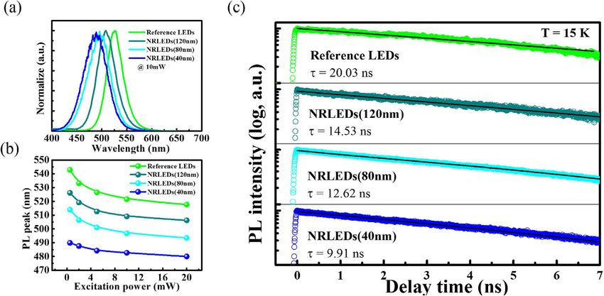
www.nature.com/scientificreports/
since the nano-ring structure has a more uniform strain distribution in the active region (we will discuss below),
the full width at half maximum (FWHM) of Reference LEDs, 120 nm, 80 nm and 40 nm (NRLEDs) were 37 nm,
42 nm, 52 nm and 51 nm, respectively. From our previously study25, the increase of carrier in the active region can
lead to the screening of the built-in field existing in the device. This screen can reduce the QCSE and move the
emission wavelength towards shorter side26. So the amount of this blue-shift can be an indicator of the original
magnitude of the built-in field. The internal strain in the device is the direct source of the QCSE and thus we can
correlate the internal strain with the amount of the blue-shift in our experiment. As shown in Fig. 3b, the amount
of blue-shift drops as the width drops, and thus the 40 nm device has a much less strain inside the ring compared
to the 120 nm case. According to coulomb screening effect theory, we can know the QCSE of NRLEDs are exactly
smaller than Reference LEDs, moreover, the NRLEDs with the wall width of 40 nm has the smallest blue-shifting
behavior. The internal quantum efficiency (IQE) behavior also be improved as decreased the wall width, as shown
in Fig. S5 (see Supplementary Note 1).
Additionally, the strain relaxation process would decrease the radiative recombination time due to improving
hole and electron wave-functions overlap and further increasing radiative recombination rate. Time-resolved PL
(TRPL) measurements performed at 300 K for ensembles of nano-rings. Figure 3c shows the PL decay time at
the PL emission peak of each sample. The radiative recombination lifetime of LEDs were 14.28 ns, 9.8 ns, 6.87 ns
and 5.49 ns for Reference LEDs, NRLEDs (120 nm), NRLEDs (80 nm) and NRLEDs (40 nm) indicated that the
radiative recombination rates are enhanced by factor of 1.5, 2.1, and 2.6, respectively, the NRLEDs have the faster
decay time, which mean the NRLEDs have a larger hole and electron wave-functions overlap than Reference
LEDs27,28. On a planar active region situation, the piezoelectric field-induced strain affect will result in band-titled
phenomenon in the active region.
From our spectral analysis, the strain released process can suppress the QCSE and cause a significant blue-shift
of PL emission peak. Therefore, in order to further understand the strain distribution of active region inside
nano-ring LEDs, we simulated the strain relaxation with the wall width reduction of a nano-ring structure by
the finite elemental method. To follow the actual etching process, we enlarge the inner circle of a nano-ring step
by step but fixed the outer diameter, as shown in Fig. 4a. In this simple model, a 3-nm-thick In0.28Ga0.72N was
sandwiched in between two GaN barriers. The strain tensors εx at the cross section of x−z plane of nano-ring
LEDs with wall width of 300 nm (Fig. 4b), 120 nm (Fig. 4c), 80 nm (Fig. 4d) and 40 nm (Fig. 4e) were calculated.
The strain tensors on both outer and inner peripheral areas show considerable relaxations at the sidewall of a
nano-ring structure. With decreasing the wall width of a nano-ring, the strain magnitude in the central region
(Black dash line in Fig. S3a) was reduced from −2.3% to −1.7% (Fig. S3b). Therefore, the better strain-relaxation
characteristic of nano-ring structures can be expected as compared to the nano-rods structure with the same
diameter (Fig. S3a,b) and the strain magnitude in active region of nano-rod and nano-ring is −2.4% and −1.7%,
respectively (Fig. S4d). In a third case, a nano-scale rod with the same diameter (40 nm) compared to the width
of the nano-ring was set up for strain calculation. In this case, the relaxation of the strain in the active region is
similar to the nano-ring case (as shown in Fig. S4c,d). As a short summary on these simulations, we found that
the rod with the same outer diameter as the nano-ring definitely bear higher strain after the etch process due to
solid nature of the structure which can preserve the difference between lattice constants of different materials.
Meanwhile much less materials are left in the nano-ring case, and this can facilitate the strain relaxation just like
the nano-rod with similar scale of material in radial direction. It can be clearly observed that the strain tensor in
the whole InGaN quantum well were reduced as the wall width of nano-ring deceases, which is attributed to the
ratio of strain-relaxed active region to the strained region size becomes larger as the diameter decreases. With
the reduced strain tensors, the suppression of QCSE can be expected. Corresponding to experimental results,
the trend of both results are similar, as shown in Fig. 4f. In Fig. 4g, the Raman peaks shift toward a lower value,
the strain is relieved in active region. Compared to the E2 phonon peak of strain-free GaN (566.5 cm−1), 1.99 and
0.73 cm−1 of the Raman peak shift correspond to 0.89 and 0.32 GPa of stress for the Reference LED and NRLED
with 40 nm wall width, respectively. According to Hooke’s law, the stress is positive correlation with strain so the
strain tendency of experiment is similar to our simulation result, as shown in Table 1 (see Supplementary Note 2).
From the simulation results, the blue-shifting behavior is not a linear tendency and it has a reverse point which
appear on roughly 100 nm. The strain relaxation here would slow down. That can explain why the blue-shifting of
our PL experimental results on 120 nm and 80 nm is almost the same in Fig. 3b.
Figure 5a shows the electroluminescence (EL) spectrum of reference LED and the NRLEDs with the wall
width of 120 nm, 80 nm and 40 nm. The EL spectrum of nana-ring LEDs would have a significant blue-shift as the
wall width of the ring reduces. The measured widest shift is 55 nm. The emission wavelength tuning capability
of nano-ring LEDs through strain engineering can be clearly observed and the color of LEDs can be tuned from
green to blue (535 nm to 480 nm), as shown in Fig. 5b. This result presents the possibility to obtain the LEDs with
different emission colors on one LED epitaxial wafer, which can be applied to micro or nano-display pixel and
multi-channel visible light communication (VLC) system.
Conclusion
In summary, we demonstrated how to fabricate the nano-ring structure with three kinds of wall widths of 120 nm,
80 nm and 40 nm. According to spectral analysis, we discovered the emission wavelength of nano-ring LEDs have
a significant shift from green to blue and the magnitude of blue-shifted was increased with decreasing the wall
width of nano-ring LEDs. Furthermore, via the TRPL measurement, when wall width of a nano-ring is decreased,
the carrier radiative recombination lifetime time was decreased due to the suppressed QCSE and increasing hole
and electron wave-functions overlap. Through the simulation of strain distribution, the results showed the strain
in the active region is relaxed. That means the reducing wall width can powerfully suppress the QCSE and modify
the emission wavelength of nano-ring LEDs. We believe this nano-ring LED design can provide a feasible solution
for the future realization of monolithic integration of RGB LEDs in nano-meter scale.
SCIENTIfIC REPOrTS | 7:42962 | DOI: 10.1038/srep42962 4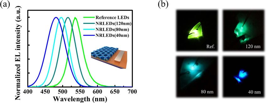
www.nature.com/scientificreports/
Figure 4. Simulating the strain variation of nano-ring active region with decreasing wall width of a ring.
The strain distribution of active region of (b) Reference LEDs and the nano-ring with (c) 120 nm (d) 80 nm and
(e) 40 nm wall width. (f) The wavelength-shifting behavior trend of simulated and experimental results. (g)
Raman spectra of Reference LED and NRLED with different wall widths.
Reference LED NR LED (120 nm) NRLED (80 nm) NRLED (40 nm)
Raman peak (cm−1) 568.49 568.10 567.42 567.23
Stress (Gpa) 0.89 0.71 0.41 0.32
Table 1. Raman shift and stress of Reference LED and NRLEDs.
Methods
Growth GaN-based materials. First, the p-type dopant in this device is Mg and carried into growth cham-
ber by Cp2Mg precursor. As we finished the growth of p-GaN, a 20 minutes of post-growth annealing will be
carried out the dopant activation. The post growth annealing was kept at 650 °C and only in N2 ambient until the
dopant was activated. The doping level is [Si] =1 × 1019 cm−3 for n-GaN and [Mg] = 1 × 1019 cm−3 for p-GaN,
respectively. The Si dopant can be nearly 100% activated but only 3% of Mg can be activated, which means that
the hole concentration is only 3 × 1017 cm−3.
ICP-RIE. A planar type ICP-RIE system is SAMCO ICPRIE 101iPH. The ICP and bias power source with RF
frequency of 13.56 MHz. The ICP system has reactor and load-lock chambers. The reaction gases of Cl2 and Ar
were introduced into reactor chamber through independent electronic mass flow controllers (MFCs) that can
precisely control the gas flow rate of each gas with about 1 standard cubic centimeter min (sccm). The etching rate
is approximately 6000 Å/min and a gas mixture condition of Cl2 and Ar is 50 and 20 sccm, respectively. During
the etching process, the ICP and bias power were maintained at 200 W with chamber pressure of 0.33 Pa.
SCIENTIfIC REPOrTS | 7:42962 | DOI: 10.1038/srep42962 5www.nature.com/scientificreports/
Figure 5. Electroluminescence (EL) characterization. (a) The EL spectrum and (b) real photograph of nano-
rings LED in different wall widths.
EL measurement. The light of the sample can be collected by a fiber. The power supplies (Keithley 2400)
can supply different currents to the sample and the spectrometer can analyze the intensity of each wavelength in
the sphere.
Numerical simulation. The electromechanical equations of nitride-based piezoelectric materials included
both the direct and the reverse piezoelectric effects. We adopt the finite element method to analyze the electro-
mechanical equations29. Since the optical properties of InGaN/GaN nanostructures depend heavily on the strain
field and the electric potential in and around MQWs, the single particle state energies of electron and hole were
calculated by using the four-band k·p Hamiltonian which includes the coupling tween the conduction band and
three valence bands29.
References
1. Bai, J., Wang, T. & Sakai, S. Influence of the quantum-well thickness on the radiative recombination of InGaN/GaN quantum well
structures. J. Appl. Phys. 88, 4729 (2000).
2. Yamamoto, S. et al. High-Efficiency Single-Quantum-Well Green and Yellow-Green Light-Emitting Diodes on Semipolar (20–21)
GaN Substrates. Appl. Phys. Express 3, 122102 (2010).
3. Lee, Y.-C., Ni, C.-H. & Chen, C.-Y. Enhancing light extraction mechanisms of GaN-based light-emitting diodes through the
integration of imprinting microstructures, patterned sapphire substrates, and surface roughness. Opt. Express 18, A489–A498
(2010).
4. Hangleiter, A. et al. Towards understanding the emission efficiency of nitride quantum wells. Phys. stat. sol. (a) 201, 2808–2813
(2004).
5. Ryou, J. H. et al. Control of Quantum-Confined Stark Effect in InGaN-Based Quantum Wells. IEEE J. Sel. Topics Quantum Electron
15, 1080–1091 (2009).
6. Sheu, J. K. et al. Low-operation voltage of InGaN-GaN light-emitting diodes with Si-doped In0.3Ga0.7N/GaN short-period
superlattice tunneling contact layer. IEEE Electron Device Lett. 22, 460–462 (2001).
7. Hardy, M. T. et al. m-Plane GaN-Based Blue Superluminescent Diodes Fabricated Using Selective Chemical Wet Etching. Appl. Phys.
Express 2, 121004 (2009).
8. Wetzel, C. et al. Light-emitting diode development on polar and non-polar GaN substrates. J. Cryst. Growth 310, 3987–3991 (2008).
9. Chen, C. et al. Ultraviolet Light Emitting Diodes Using Non-Polar a-Plane GaN-AlGaN Multiple Quantum Wells. Jpn. J. Appl. Phys.
42, L1039–L1040 (2003).
10. Shervin, S. et al. Bendable III-N Visible Light-Emitting Diodes beyond Mechanical Flexibility: Theoretical Study on Quantum
Efficiency Improvement and Color Tunability by External Strain. ACS Photonics 3, 486–493 (2016).
11. Li, S. & Waag, A. GaN based nanorods for solid state lighting. Jpn. J. Appl. Phys. 111, 071101 (2012).
12. Tourbot, G. et al. Growth mechanism and properties of InGaN insertions in GaN nanowires. Nanotechnology 23, 135703 (2012).
13. Chichibu, S. F. et al. Effective band gap inhomogeneity and piezoelectric field in InGaN/GaN multiquantum well structures. Appl.
Phys. Lett. 73, 2006 (1998).
14. Adelmann, C. et al. Growth and optical properties of GaN/AlN quantum wells. Appl. Phys. Lett. 82, 4154 (2003).
15. Koester, R. et al. High-speed GaN/GaInN nanowire array light-emitting diode on silicon (111). Nano Lett. 15, 2318–2323 (2015).
16. Yohei, E. et al. 531 nm Green Lasing of InGaN Based Laser Diodes on Semi-Polar {2021} Free-Standing GaN Substrates. Appl. Phys.
Express 2, 082101 (2009).
17. Bai, J., Wang, Q. & Wang, T. Characterization of InGaN-based nanorod light emitting diodes with different indium compositions. J.
Appl. Phys. 111, 113103 (2012).
18. Wang, Q., Bai, J., Gong, Y. P. & Wang, T. Influence of strain relaxation on the optical properties of InGaN/GaN multiple quantum
well nanorods. J. Phys. D: Appl. Phys. 44, 395102 (2011).
19. Ke, M. Y. et al. Application of Nanosphere Lithography to LED Surface Texturing and to the Fabrication of Nanorod LED Arrays.
IEEE J. Sel. Topics Quantum Electron. 15, 1242–1249 (2009).
20. Yun, D.-S., Lee, H.-S., Jang, H.-G. & Yoo, J.-W. Controlling Size and Distribution for Nano-sized Polystyrene Spheres. Bull. Korean
Chem. Soc. 31, 1345–1348 (2010).
21. Teng, C.-H., Zhang, L., Deng, H. & Ku, P.-C. Strain-induced red-green-blue wavelength tuning in InGaN quantum wells. Appl. Phys.
Lett. 108, 071104 (2016).
22. Kawakami, Y. et al. Optical properties of InGaN/GaN nanopillars fabricated by postgrowth chemically assisted ion beam etching. J.
Appl. Phys. 107, 023522 (2010).
SCIENTIfIC REPOrTS | 7:42962 | DOI: 10.1038/srep42962 6www.nature.com/scientificreports/
23. Takeuchi, T. et al. Quantum-confined Stark effect due to piezoelectric fields in GaInN strained quantum wells. Jpn. J. Appl. Phys. 36,
L382 (1997).
24. Bernardini, F., Fiorentini, V. & Vanderbilt, D. Spontaneous polarization and piezoelectric constants of III-V nitrides. Phys. Rev. B 56,
R10024 (1997).
25. Lee, Y.-J. et al. Study of the excitation power dependent internal quantum efficiency in InGaN/GaN LEDs grown on patterned
sapphire substrate. IEEE J. Sel. Topics Quantum Electron. 15, 1137–1143 (2009).
26. Kuroda, T. & Tackeuchi, A. Influence of free carrier screening on the luminescence energy shift and carrier lifetime of InGaN
quantum wells. J. Appl. Phys. 92, 3071 (2002).
27. Lefebvre, P. et al. Time-resolved photoluminescence as a probe of internal electric fields in GaN-(GaAl) N quantum wells. Phys. Rev.
B 59, 15363 (1999).
28. Im, J. S. et al. Reduction of oscillator strength due to piezoelectric fields in G a N/A l x Ga 1−x N quantum wells. Phys. Rev. B 57,
R9435 (1998).
29. Hong, K. B. & Kuo, M. K. Fully coupled and semi-coupled piezoelectric models on the optical properties of InGaN quantum dots.
Semicond. Sci. Technol. 25, 065005 (2010).
Acknowledgements
The authors express their gratitude to Epistar for providing technical support. This research was funded by the
Ministry of Science and Technology of Republic of China under grant number, MOST 104-3113-E-009-002-CC2.
Author Contributions
S.W.W., K.B.H. and C.H.T. conceived and designed this study. Y.L.T., A.J.T. and Y.C.C. performed the experiment.
S.W.W. and K.B.H. performed the numerical simulation and modelling. S.W.W., P.T.L., Y.L.T. and A.J.T. analyzed
the data. S.W.W., K.B.H., P.C.K, C.C.L., and H.C.K. wrote the paper. All authors reviewed the final manuscript.
Additional Information
Supplementary information accompanies this paper at http://www.nature.com/srep
Competing financial interests: The authors declare no competing financial interests.
How to cite this article: Wang, S.-W. et al. Wavelength tunable InGaN/GaN nano-ring LEDs via nano-sphere
lithography. Sci. Rep. 7, 42962; doi: 10.1038/srep42962 (2017).
Publisher's note: Springer Nature remains neutral with regard to jurisdictional claims in published maps and
institutional affiliations.
This work is licensed under a Creative Commons Attribution 4.0 International License. The images
or other third party material in this article are included in the article’s Creative Commons license,
unless indicated otherwise in the credit line; if the material is not included under the Creative Commons license,
users will need to obtain permission from the license holder to reproduce the material. To view a copy of this
license, visit http://creativecommons.org/licenses/by/4.0/
© The Author(s) 2017
SCIENTIfIC REPOrTS | 7:42962 | DOI: 10.1038/srep42962 7You can also read