10 Flexible and Stretchable Devices from Unconventional 3D Structural Design - Sites at USC
←
→
Page content transcription
If your browser does not render page correctly, please read the page content below
165

10

Flexible and Stretchable Devices from Unconventional
3D Structural Design
Hangbo Zhao and Mengdi Han
Northwestern University, Center for Bio-Integrated Electronics, Evanston, IL, USA

Many biological systems in nature are three-dimensional (3D), such as plant
roots, animal cells, human vascular networks, etc. The 3D feature provides
essential functions in various activities including physicochemical reactions and
interactions with the environment. Biomimetic recreation and engineering of
3D architectures inspired by nature has been a topic of increasing interest in
recent decades, especially in the area of flexible and stretchable devices. 3D
structures on such devices enable new and more complex functionalities as
compared to 1D or 2D counterparts. Moreover, the flexibility and stretchability
of the substrate provide a unique means of forming, controlling, and tuning
3D structures on it. The interplay between mechanics and structures provides
plenty of space and fascinating opportunities for the design and fabrication of
unconventional 3D structures with novel functionalities.
  In this chapter, various approaches to forming unconventional 3D struc-
tures are first introduced, from basic buckling of ribbons, membranes, and
non-coplanar bridge-island structures, to more complex deterministic assembly.
A series of strategies for extending the level of control in deterministic assembly
is discussed, followed by a collection of exemplary flexible and stretchable
electronic and optical devices fabricated using 3D deterministic assembly
methods.

10.1 Stretchable 3D Ribbon and Membrane Structures
Formed by Basic Buckling
Mechanical buckling of thin films under compressive stress provides a power-
ful route to forming 3D structures. The stretchability of elastomeric substrates
is utilized as a platform for buckling micro-/nanostructures. In this section, the
fabrication of 3D ribbon and membrane structures based on simple substrate
buckling is introduced.

Flexible and Stretchable Triboelectric Nanogenerator Devices: Toward Self-powered Systems,
First Edition. Edited by Mengdi Han, Xiaosheng Zhang, and Haixia Zhang.
© 2019 Wiley-VCH Verlag GmbH & Co. KGaA. Published 2019 by Wiley-VCH Verlag GmbH & Co. KGaA.
166   10 Flexible and Stretchable Devices from Unconventional 3D Structural Design

      10.1.1                3D Nanoribbons
      The John A. Rogers group from the University of Illinois Urbana-Champaign
      exploited compressive buckling to convert nanoribbons into 3D, wavy structures.
      The process starts with fabricating patterned thin, flat, single-crystal silicon rib-
      bons on a mother wafer [1]. Then, the Si elements are bound to a pre-strained
      elastomeric substrate. After peeling off the elastomer and releasing the pre-strain,
      the silicon is transformed into well-controlled, periodic wavy ribbons that are
      stretchable. Large-area, uniform-array, wavy nanoribbons can be fabricated using
      this method. The nanoribbons are highly stretchable, with a maximum strain over
      10% for both compression and stretching. A single-crystal silicon p–n diode is
      showcased as an example of applications of such wavy nanoribbons.
        The same principle of buckling nanoribbons could be applied with spatial con-
      trol over adhesion sites added to create well-controlled local displacement of the
      ribbons [2]. The fabrication process is schematically illustrated in Figure 10.1a.

      (a)                                                                                 (b)
                                                SU8 5
                                                Gold
                                                Quartz
                                                                                                                          Stretch                Compress
                    Photolithography
            (i)
                    and gold etching
                                                                                          (c)
                                                             (vi)     Cast PDMS
                                                UVO
                                                mask
                                                                                                                                                                10 μm
                      Win     Wact
                    Laminate UVO mask
            (ii)
                    against stretched PDMS
                        UV light
                                                             (v)      Release PDMS
                                                Air                                  GaAs
                                                panel
                            L + ΔL            PDMS
            (iii)
                    Expose to UV light and                               L + ΔL                                                                               100 μm
                    removal of mask
                                          Activated
                                                                      Bond GsAs ribbons
                                          surface            (iv)     to pre-strained
                                                                      PDMS

      (d)                                                                                   (e)
                                                                                                            6.0
        GaAs                                                                         Au
                                                                                                                  Stretching degree
                                                 PDMS                                                       4.0            0%
                                                                                                                        14.4%
                                                                                                            2.0         34.3%
                                                                                            Current (μA)

                                       V                          A                                                     44.4%
                                                                                                                        51.4%
                                                                                                            0.0
                                                 GaAs
                                                                                                           –2.0
                                           Infrared irradiation

                                                                                                           –4.0
                                                                                                                                            With light illumination
                                                                                                           –6.0
                                                                                                                  –0.4      –0.2          0.0          0.2    0.4
                Au/GaAs                           GaAs                      Au/GaAs                                                 Bias voltage (V)

      Figure 10.1 Buckling of semiconductor nanoribbons for stretchable electronics. (a) Schematic
      illustration of the fabrication process of 3D buckled nanoribbons. (b) Schematic of bucked
      nanoribbons in response to stretching and compression. (c) SEM image of GaAs nanoribbons
      formed. (d) Schematic and optical images of a stretchable photodetector (PD) from
      nanoribbons. (e) I–V characteristics of fabricated PDs under different stretching degrees.
      Source: Reproduced with permission from Sun et al. [2]. Copyright 2006, Springer Nature.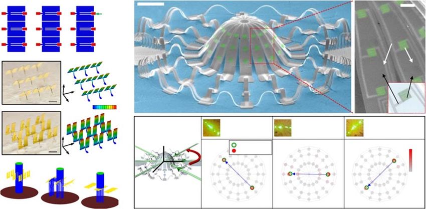
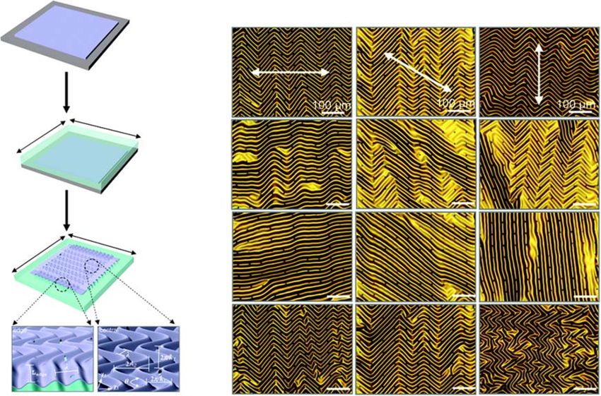
10.2 Deterministic 3D Assembly   167

An ultraviolet ozone (UVO) mask is used to pattern the surface chemistry on
a poly(dimethylsiloxane) (PDMS) substrate, where bonding between the Si or
GaAs nanoribbons and PDMS substrate only occurs in lithographically defined
regions. The buckled nanoribbons could be embedded in PDMS and undergo
extremely high levels of stretching (up to ∼100%), compression (up to ∼25%),
and bending (with curvature radius down to ∼5 mm), as shown in Figure 10.1b.
  Such stretchable ribbons could be used in the construction of metal–semi-
conductor–metal photodetectors, as shown in Figure 10.1c–e. The I–V charac-
teristics of the photodetectors are mechanically tunable due to the change of the
projected area of the buckled GaAs ribbons.

10.1.2   3D Nanomembranes
In addition to nanoribbons, nanomembranes could also be engineered into 3D
configurations using buckling. As shown in Figure 10.2, a silicon thin film, ini-
tially on a mother wafer, is transferred to a biaxially pre-strained PDMS slab.
After the release of the strain of PDMS, wavy Si nanomembranes are formed with
controllable surface topologies.
   The formed wavy Si nanomembranes are stretchable, and yield various
morphologies in response to different strains applied at different orientations, as
shown in Figure 10.2b. These wavy membranes provide a useful path to biaxially
stretchable devices.

10.1.3   3D Bridge-Island Structures
More complex structural configurations are achievable by combining ribbons
with island-like 2D structures. Figure 10.3 shows an example of non-coplanar,
bridge-island structures [4]. The ultrathin circuit mesh fabricated using standard
semiconductor fabrication is bound to pre-stretched PDMS at the positions of the
flat islands, via ozone surface treatment. Using this strategy, an array of comple-
mentary metal–oxide–semiconductor (CMOS) inverters is fabricated and encap-
sulated with PDMS (Figure 10.3b). The fabricated device offers extremely high
stretchability, with stretching strain up to ∼140% and twisting pitch as tight as
90∘ in ∼1 cm (Figure 10.3c).
  The feature size of the stretchable circuit is comparable to conventional 2D
devices, while no significant changes in electrical properties are observed owing
to the high stretchability of the PDMS substrate and mechanics-guided structural
design.

10.2 Deterministic 3D Assembly
While the basic buckling approaches described in Section 10.1 are effective
in transforming 2D patterns into 3D configurations, the accessible structures
are limited to wavy ribbons, membranes, and combinations of them. In this
section, a more complex 3D assembly approach is introduced, namely, deter-
ministic 3D assembly. Deterministic 3D assembly combines lithographically
Fabricate thin Si membrane film

                                                                (i)             (ii)                     (iii)

                                      Mother wafer
                                                                                                                                Stretching strain

                                                                                                                                εst = 0%
                            Contact and transfer to
                            pre-strained PDMS slab
                                                                       100 μm                   100 μm                 100 μm
                               L+Δ
                        L             L
                  L   +Δ

                                                                                                                                εst = +1.8%

                            Peel off the PDMS slab; flip over
                            and release the strain of PDMS

                                  L
                                                                                                                                εst = +3.8%
                  L

                                                                                                                                εst = 0%

            (a)                                                 (b)

Figure 10.2 Biaxially stretchable “wavy” nanomembranes. (a) Schematic illustration of the fabrication process. (b) Optical micrographs of wavy Si
nanomembranes under different uniaxial strains at three different orientations. Source: Reproduced with permission from Choi et al. [3]. Copyright 2007,
American Chemical Society.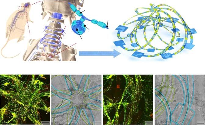
10.2 Deterministic 3D Assembly   169

        Fabricate ultrathin
        circuit mesh
                                                                     300 μm

                           Wafer
      Liftoff; deposit Cr/SiO2

                                      Deform/
                                      release                        200 μm
      Transfer fo stretched PDMS

                         PDMS
      Encapsulate with PDMS
(a)                                   (b)

                                                            1 mm

           100 μm

                      Twist

               Diag. stretch       Bend/stretch
  (c)

Figure 10.3 Stretchable, noncoplanar electronics. (a) Schematic illustration of the fabrication
process for circuits with bridge-island structures. (b) SEM images of an array of CMOS inverters
fabricated using the method in (a). (c) Optical image of CMOS inverter arrays under large
deformation including stretching, twisting, and bending. Source: Reproduced with permission
from Kim et al. [4]. Copyright 2008, PNAS.

controlled layouts of 2D structures with patterned adhesion sites to the surface
of pre-strained elastomer substrates to enable fast and scalable assembly of a
broad range of 3D structures.

10.2.1       Basic Approach of Deterministic 3D Assembly
The basic approach of deterministic 3D assembly is described in detail in Refs.
[5–7]. Briefly, the process starts with patterning 2D patterns (precursors) with
lithographically defined bonding sites. Then, the 2D precursors are bound
to a pre-stretched elastomer slab. Release of the pre-strain induces spatially
dependent twisting and bending deformations, transforming the 2D patterns
into 3D structures.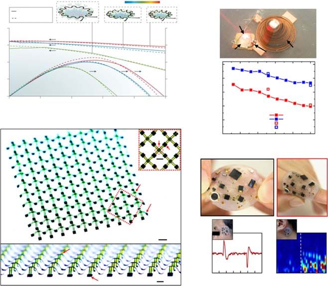
170 10 Flexible and Stretchable Devices from Unconventional 3D Structural Design
Form 2D precursor structures; Figure 10.4 Schematic
stretch the assembly platform illustration of the assembly
approach for forming 3D conical
2D coils of single-crystalline Si.
m Source: Reproduced with
icr
o- permission from Yan et al. [6].
/n
an Copyright 2017, Elsevier.
os
tru
Fr ct
ee ur
-s es
ta
nd
in
g
sil
ico
ne
Transfer with selective bonding
Bo
nd
in
g
sit
St es
re
tc
he
d
sil
ico
ne
Re
le Release the platform
as
ed
sil
ico
ne
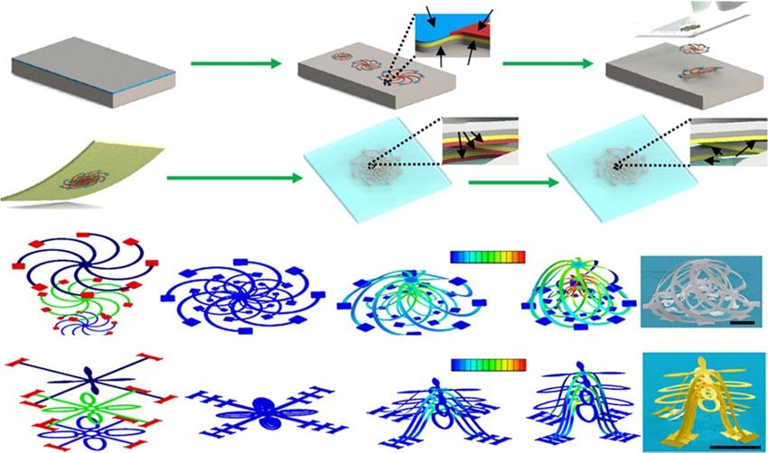
As shown in Figure 10.4, 3D conical helices made from single-crystal silicon are
fabricated, which were inaccessible 3D architectures previously. The mechanics
and shape transformation process can be analyzed and precisely predicted by a
finite element analysis (FEA) scheme, and excellent agreement is found between
FEA predictions and experiments. A broad class of geometries are realized,
including single and multiple helices, conical spirals, flowers, frameworks, and
multilevel configurations. Moreover, this 3D assembly approach applies to var-
ious material compositions (inorganic semiconductors, polymers, metals, and
heterogeneous combinations) and feature sizes (submicrometer to centimeter),
as shown in Figure 10.5.
This deterministic 3D assembly approach provides a powerful route to sophis-
ticated classes of 3D structures and materials. The compatibility with the CMOS
fabrication methods, and device-grade materials, creates many opportunities for
achieving new 3D-structure-based electronic and other devices.
Depending on the basic 3D assembly method described in the previous
sections, a series of strategies and processing techniques have been developed to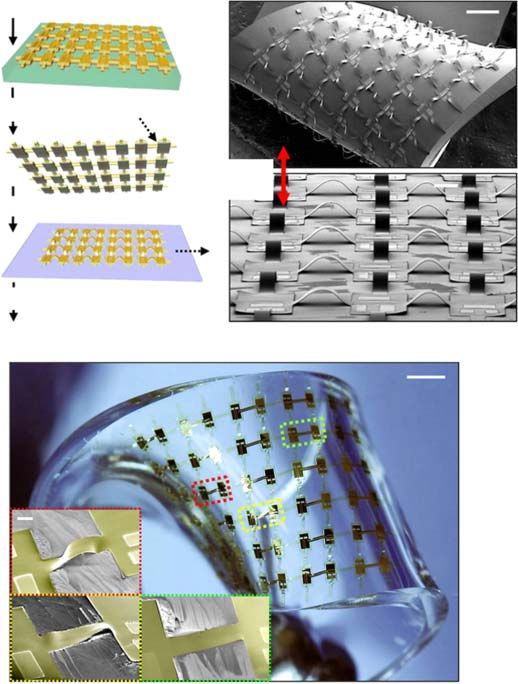
5 μm                        200 μm                                                                                     20 cm

                                                                               5 mm                           2 cm

          Sub-microscale                Microscale                  Millimeter scale              Centimeter scale                 Meter scale

                      5 μm                     200 μm                         5 mm                            2 cm                       20 cm

                 Blood cells
    (a)

       SU8                      Pl                      Ni              Au                    SU8–Au              SU8–Si          SU8–Si nanodiscs

                                                                                                                                                    1 μm

    (b)

Figure 10.5 3D structures fabricated using the deterministic 3D assembly approach with various characteristic dimensions and materials. (a) Starfish-
jellyfish-like structures. (b) 3D mesostructures of different materials. Source: Reproduced with permission from Zhang et al. [8]. Copyright 2017, Springer
Nature.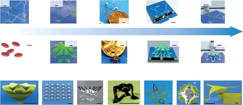
172 10 Flexible and Stretchable Devices from Unconventional 3D Structural Design
extend the level of control in the deterministic 3D assembly process, which has
greatly increased the space of attainable 3D structures.
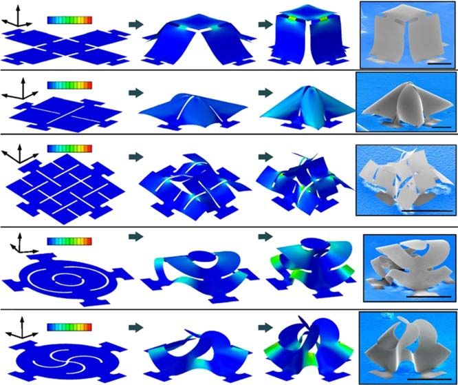
10.2.2 3D Kirigami Structure in Micro-/Nanomembranes
The John A. Rogers group from the University of Illinois Urbana-Champaign
introduced the concept of kirigami to the 3D assembly method, where 2D
micro-/nanomembranes have strategically designed geometries and pat-
terns of cuts [9]. Figure 10.6 lists several examples showing how the 2D
silicon membranes with engineered kirigami cuts at precisely defined loca-
tions are transformed into 3D structures with strategically determined panel
deformations.
10.2.3 Buckling Control Assisted by Stress and Strain Engineering
Engineering of stress and strain in the 2D precursors could also influence the
3D buckling process. Figure 10.7 shows two such engineering strategies. In
Figure 10.7a, residual stress is introduced to the 2D precursor by patterning a
2D silicon membrane Partially assembled 3D structure 3D structure Experiment
z εmax (%)
y x
0.0 0.8
(a)
εmax (%)
z
y x
0.0 1.4
(b)
εmax (%)
z x
y 0.0 1.4
(c)
z εmax (%)
y x 0.0 0.9
(d)
z εmax (%)
y x
0.0 1.2
(e)
Figure 10.6 Examples of mechanically driven kirigami for deterministic 3D assembly from 2D
micro/nanomembranes. (a) A square cuboid. (b,c) Membranes with first- and second-order
cross-cuts. (d,e) Membranes with symmetric and antisymmetric cuts. Scale bars, 200 μm.
Source: Reproduced with permission from Zhang et al. [9]. Copyright 2015, PNAS.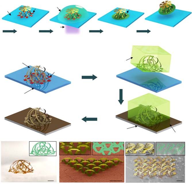
10.2 Deterministic 3D Assembly          173

                              Tensile           FEM
                              residual stress
  εpre = 80%                   σresidual = +480 MPa

                                           Analytical
                     2.16 mm

                                                        εrelease = 30%                       60%                         100%
                               Compressive
                               residual stress FEM
       1.8 mm                  σresidual = –580 MPa

                                          Analytical

 (a)

                z
                                                                                                                               Transfer print sample
          x         y                                                                                                             onto PVA tape

                        old
                    te m
              stra
         Sub
 Form engineered                                                                  εmax-ribbon (%)
 substrate on mold                                              trate                                 0.04
                                                          ds ubs                  0.0
                                                     tche                      rsor
                                                                                        s
                                                 Stre                         u
                                                                    2D   prec
                                εmax-substrate                                                                             Form 2D Si/SU8 patterns
                                                                                                                             by photolithography
                              0.00         0.69
Pre-stretch engineered                                                                                       s                     εmax-ribbon (%)
                                                                                                        ture
                                                                                                 truc
substrate (60% strain);                                                                      3D s                                  0.0          2.8
  align sample onto
       substrate                                                                                                                 ure s
                                                                                                                            ruct
                    Laminate sample with                                                                         trate 3D st
                                                                                                         ubs
                        selective bonding                                                        as ed s
                                                                                            Rele
                                                        Release the substrate    εmax-substrate
                                                        to form 3D structures 0.00          0.62

 (b)

Figure 10.7 Buckling control assisted by stress and strain engineering. (a) Stress engineering.
(b) Strain engineering. SOI, silicon on insulator; PVA, poly(vinyl alcohol). Source: Reproduced
with permission from Fu et al. [10] and Nan et al. [11].

2D SiNx film onto a Si substrate prior to the 2D precursors being buckled [10].
This residual stress, either tensile or compressive, induces different buckling
mechanics and results in distinct 3D structures.
   Another strategy involves the engineering of elastomer substrates for spatially
nonuniform strain in the substrates for buckling. As Figure 10.7b illustrates, the
elastomer substrate, which is nonuniform in thickness via molding, induces spa-
tially varying strain upon release of the pre-strain, thereby creating nonuniform
3D structures [11]. A similar strain-engineered method is also used to fabricate
3D microarchitectures based on growth [12].

10.2.4          Multilayer 3D Structures
Instead of single-layered structures, multilayers of advanced materials could
also be produced using releasable, multilayer 2D precursors. The schematic
illustration of the process is shown in Figure 10.8a [13]. Multilayer 2D precursors
are transferred to the stretched elastomer using a layer-by-layer transfer printing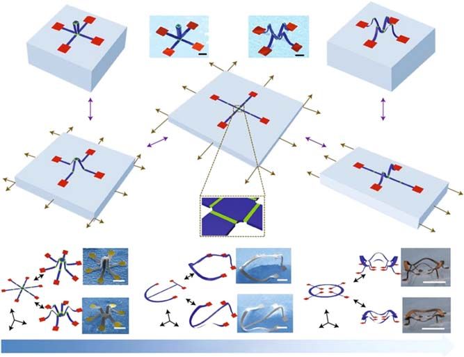
SiO2              AZ 5214
                                                                                                                                            p
                                                                                                                                        Stam
                                             Fabricate 2D                                                              Layer-by-layer
                                             presursors                                                                transfer

                                                                                                     Si     SU8

                SOI wafer

                                                                                                          AZ 5214
                                         Laminate samples on
                            PVA tape     pre-stretched elastomer                                                                                Gap
                                                                                                       er
                                                                                                     om
                                         Dissolve PVA tape                                  e   last               Remove
                                                                                       ed
                                                                                 tch                               AZ 5214
                                                                          Stre
          (a)
                                                                                                                εmax (%)

                                                                                                          0.0              0.27

          (b)                                                                                                   εmax (%)

                                                                                                          0.0              4.33

          (c)

Figure 10.8 Deterministic assembly of 3D mesostructures from multilayer 2D precursors. (a) Schematic illustration of the fabrication process. (b and c)
Examples of resulting 3D multilayer structures. Scale bars, 400 μm. Source: Reproduced with permission from Yan et al. [13]. Copyright 2016, AAAS.
10.2 Deterministic 3D Assembly 175
technique. Complex 3D topologies such as dense architectures with nested
layouts are constructed (Figure 10.8b,c). The multilayer feature also enhances
the structural stability and drives the motion of extended features in those
structures.
10.2.5 Freestanding 3D Structures
A potential disadvantage of the 3D assembly method discussed so far is that the
elastomeric substrates, necessary for the assembly process, could impose engi-
neering constraints to the system as the 3D structures are mechanically tethered
to the substrates. Several techniques have been developed to bypass this limita-
tion in order to fabricate freestanding 3D structures, including interfacial pho-
topolymerization and wax-assisted transfer [14].
The process of interfacial photopolymerization is schematically shown in
Figure 10.9a. A thin, sacrificial Al2 O3 layer is deposited between the bonding sites
Assembly Al2O3 SU8 droplet SU8 base
substrate
UV light
Assemble 3D structures Drop cast SU8 Backside exposure Release
(a)
Assembled
3D structures Wax
Drop wax
Al2O3 and release
Assembly Transfer
substrate print
Dissolve
wax
Target
substrate
Adhesive layer
Quartz substrate Copper substrate Silicon substrate
(b)
Figure 10.9 Freestanding 3D structures. (a) Interfacial photopolymerization and
(b) wax-assisted transfer printing methods for fabricating freestanding 3D structures
assembled by compressive buckling. Scale bars, 500 μm. Source: Reproduced with permission
from Yan et al. [14]. Copyright 2017, PNAS.176 10 Flexible and Stretchable Devices from Unconventional 3D Structural Design
and the elastomer for subsequent release from the substrate. To mechanically
hold the 3D deformed shape, a photodefinable epoxy SU8 is cast and cured
onto the 3D structure, followed by patterned backside exposure. Developing
of the epoxy and removal of the Al2 O3 layer releases the 3D structures into
freestanding objects, with a thin remaining base layer.
For the second method shown in Figure 10.9b, transfer printing is employed,
assisted by wax encapsulation to transfer the assembled 3D structures onto the
target substrate. The wax holds the shape of the deformed structures and is
dissolved upon transfer of the structures onto the adhesive layer on the target
substrate.
10.2.6 Morphable 3D Structures by Multistable Buckling Mechanics
3D structures that can undergo reversible transformations are important in a
broad range of applications such as microelectromechanical systems (MEMSs),
biomedical devices, and microrobotics. A scheme in 3D assembly was developed
recently to fabricate morphable 3D structures relying on sequential release of the
pre-strain in elastomeric substrates [15].
The concept of the scheme and representative SEM images are illustrated
in Figure 10.10a,b, respectively. Starting from a biaxially stretched flat state of
Shape I Shape II
Experiment
εx = 0% εx = 0%
εy = 0% εy = 0%
εx = 100%
εy = 100%
Flat state
εx = 50% εx = 0%
εy = 50% εy = 100%
Intermediate state I Crease Intermediate state II
(a)
z z z
y x y y
x x
Micrometers (SU8 + silicon) Tens of micrometers (silicon) Millimeter (PET + Cu)
(b)
Figure 10.10 Morphable 3D structures by loading-path-controlled mechanical assembly.
(a) Schematic illustration of the strategy with FEA predictions and experimental SEM images of
formed 3D structures. (b) 2D shapes, FEA predictions, and corresponding experimental images
of morphable 3D structures. Scale bars, 1 mm. Source: Reproduced with permission from Fu
et al. [15]. Copyright 2018, Springer Nature.10.3 Flexible and Stretchable Devices from 3D Assembly 177 the substrate, the pre-strain could be released in two different loading paths: simultaneous release in both x and y directions or sequential release (y direction first, then x direction). These two loading paths yield two distinct buckling modes and corresponding 3D structures due to the mechanics involved in the buckling process. The entire process is reversible, and thereby the two shape configurations can be switched between each other continuously and repetitively. Again, such reconfigurable 3D structures are achievable in a broad set of materials, multilayer stacks, and over various length scales. 10.3 Flexible and Stretchable Devices from 3D Assembly The deterministic 3D assembly method discussed in Section 10.2 provides a ver- satile route to the fabrication of 3D structures made of a broad range of materials, complex geometric configurations, and over various length scales. Such 3D struc- tures are integrated on elastomeric substrates upon assembly, making them capa- ble of dynamically and reversibly changing their shapes. This feature makes them promising building blocks for flexible and stretchable devices for applications spanning from microelectronic, to optical, optoelectronic, and biomedical appli- cations. In this section, some exemplary flexible and stretchable devices fabri- cated using the deterministic 3D assembly are introduced. 10.3.1 Electronic Devices and Systems As the fabrication process of the 2D precursors is compatible with the most sophisticated CMOS process, a variety of classes of electronic components, devices, and systems could be made on the basis of the 3D assembly method. Furthermore, the mechanical tunability of the 3D structures gives rise to tunable electronic properties of such flexible devices [8, 13–19]. Several exemplary electronics devices and systems are shown in Figure 10.11. A 3D toroidal inductor is fabricated and can be mechanically configured into two distinct shapes by partial and then complete release of the pre-strain (Figure 10.11a) [8]. Good agreement between the FEA-predicted and experi- mentally measured inductance as a function of frequency is observed. In Figure 10.11b, a pyramidal coil is fabricated as part of a 3D NFC device taking advantage of the multilayer stacking strategy [13]. The 3D NFC device exhibits significantly enhanced Q factor and improved working angle over conventional 2D counterparts. Figure 10.11c shows a network of Si-nanomembrane-based nMOS transistors interconnected by bridge structures [16]. Helical coils fabricated using compres- sive buckling are used as effective electrical interconnects for soft electronics, as shown in Figure 10.11d [17]. 10.3.2 Optical and Optoelectronic Devices Complex 3D structures inspired by origami and kirigami are promising plat- forms for optical and optoelectronic applications. For example, a mechanically
178 10 Flexible and Stretchable Devices from Unconventional 3D Structural Design
H (A/m)
1 300
Measurement
Modeling
LED
8 4
Inductance (nH)
6 3
NFC chip 3D coil
Q factor
Capacitor
4 2 25
3D coil
2 1 20
Q factor
15 2D coil
0 0
0 2 4 6 8 10
10
Frequency (GHz)
Modeling
(a) 5
Experiment
0
nMOS 0.0 0.4 0.8 1.2 1.6 2.0
(b) Width of supporting ribbon wribbon (mm)
Bonding
site
500 μm
nMOS
Bonding site
EOG EEG
14
1
1 mm Eyes
Amplitude (mV)
Frequency (Hz)
Downside closed
Eyes
nMOS
opened
0 12
Upside
–1 10
0 1 2 3 4 5 6 7 0 1 2 3 4
Bonding site 500 μm Time Time
(c) (d)
Figure 10.11 Exemplary flexible electronic devices fabricated using deterministic 3D
assembly. (a) Measured and modeled frequency dependence of the inductance and Q factor of
a 3D torsional inductor. Source: Reproduced with permission from Zhang et al. [8]. Copyright
2017, Springer Nature. (b) A 3D NFC device with enhanced Q factor over conventional 2D
counterparts. Source: Reproduced with permission from Yan et al. [13]. Copyright 2016, AAAS.
(c) A 3D-interconnected bridge structure with an array of Si nanomembrane nMOS transistors.
Source: Reproduced with permission from Kim et al. [16]. Copyright 2018, American Chemical
Society. (d) A flexible device composed of a network of helical coils as electrical interconnects.
Source: Reproduced with permission from Jang et al. [17]. Copyright 2018, Springer Nature.
tunable optical transmission window is demonstrated in Figure 10.12a [9]. As the
membrane rotates in response to the strain applied to the elastomer substrate,
the amount of normally incident light they block also changes continuously,
making the device an optical shutter with well-controlled mechanical tunability.
In Figure 10.12b, a 3D hemispherical structure is made by integrating 2D mate-
rials (graphene, MoS2 ) with a buckled hemispherical 3D structure [20]. The 2D
semiconductor/semimetal materials provide photodetection and light-imaging
capabilities on the 3D structural platform.
10.3.3 Scaffolds as Interfaces with Biological Systems
3D structures formed by compressive 3D assembly could also serve as electronic
cellular scaffolds for the growth, recording the stimulation of neural networks.2D precursor (design I, 90% pre-strain)
Bonding 1 mm 100 μm
region
SU-8
Partially assembled 3D structure
Experiment FEA
Graphene MoS2
z
y
x uz (μm)
3D optical transmission window SU-8
0 855
θ = –45.0°, ϕ = 90.0° θ = 0.0°, ϕ = 90.0° θ = 45.0°, ϕ = 90.0°
θ = –45.0°, ϕ = 90.3° θ = –1.1°, ϕ = 91.1° θ = 44.3°, ϕ = 91.3°
z (iii)
y Z (i) (ii) (iii) lph
Using protractor
x P2 Experimental 1 μA
P1
εappl = 0% Light spot X
(ii) P2 P1
43% 0
Optical 66%
shutter y
(i)
P1
θ = –45°→0°→45° P2
Receiver ϕ = 0°
(a) (b)
Figure 10.12 An exemplary flexible 3D-structure-based device for optical and optoelectronic applications. (a) A mechanically tunable optical shutter. Scale
bars, 500 μm. Source: Reproduced with permission from Zhang et al. [9]. Copyright 2015, PNAS. (b) A 3D photodetection and imaging system. Source:
Reproduced with permission from Lee et al. [20]. Copyright 2018, Springer Nature.180 10 Flexible and Stretchable Devices from Unconventional 3D Structural Design
Schwann cell
Axon
Satellite cell
Pseudounipolar
neuron
Culture on 3D scaffolds
(a)
(b)
Figure 10.13 3D electronic scaffolds for engineering neural network. (a) Schematic illustration
of rat dorsal root ganglion (DRG) and cell populations on 3D structures. (b) Confocal
fluorescence micrographs of DRG cells cultured on a 3D cage structure. Scale bars, 100 μm.
Source: Reproduced with permission from Yan et al. [14]. Copyright 2017, PNAS.
Figure 10.13 shows an example of a freestanding 3D open-cage structure used
as scaffold for engineered dorsal root ganglion (DRG) neural networks [14]. The
3D configuration allows interaction and communication with live cells and tis-
sues in 3D. Experiments demonstrate that such scaffolds facilitate the reorgani-
zation of cells into hierarchical cellular constructs. This example shows promising
opportunities of 3D structures as cellular and tissue scaffolds in fundamental and
applied biological studies.
10.4 Summary
This chapter introduces different approaches for forming 3D structures. Bonding
nanomembranes in Si or other inorganic materials to a pre-strained elastomer
can yield 3D wavy structures with controllable surface topologies upon release of
the pre-strain. On this basis, deterministic 3D assembly introduces spatial con-
trol of the adhesion sites to further expand the accessible 3D geometries. The
final 3D geometries can be tailored through layouts of the 2D patterns, position
of the bonding sites, pre-strains, thickness profiles of 2D patterns, loading path,
nonuniform elastomeric substrates, and many others. Applications of such 3D
mesostructures cover the field of electronics, optoelectronics, optical devices,
biointerfaces, energy harvesters, microrobots, and others.References 181
Abbreviations
CMOS complementary metal–oxide–semiconductor
FEA finite element analysis
MEMS microelectromechanical system
NFC near-field communication
PDMS poly(dimethylsiloxane)
SEM scanning electron microscopy
References
1 Khang, D.-Y., Jiang, H., Huang, Y., and Rogers, J.A. (2006). A stretchable form
of single-crystal silicon for high-performance electronics on rubber substrates.
Science 311: 208–212.
2 Sun, Y., Choi, W.M., Jiang, H. et al. (2006). Controlled buckling of semicon-
ductor nanoribbons for stretchable electronics. Nature Nanotechnology 1:
201–207.
3 Choi, W.M., Song, J., Khang, D.-Y. et al. (2007). Biaxially stretchable “wavy”
silicon nanomembranes. Nano Letters 7: 1655–1663.
4 Kim, D.-H., Song, J., Choi, W.M. et al. (2008). Materials and noncoplanar
mesh designs for integrated circuits with linear elastic responses to extreme
mechanical deformations. Proceedings of the National Academy of Sciences of
the United States of America 105: 18675–18680.
5 Xu, S., Yan, Z., Jang, K.-I. et al. (2015). Assembly of micro/nanomaterials into
complex, three-dimensional architectures by compressive buckling. Science
347: 154–159.
6 Yan, Z., Han, M., Yang, Y. et al. (2017). Deterministic assembly of 3D
mesostructures in advanced materials via compressive buckling: a short
review of recent progress. Extreme Mechanics Letters 11: 96–101.
7 Liu, W., Zou, Q., Zheng, C., and Jin, C. (2019). Metal-assisted transfer strat-
egy for construction of 2D and 3D nanostructures on an elastic substrate.
ACS Nano 13: 440–448.
8 Zhang, Y., Zhang, F., Yan, Z. et al. (2017). Printing, folding and assembly
methods for forming 3D mesostructures in advanced materials. Nature
Reviews Materials 2: 17019.
9 Zhang, Y., Yan, Z., Nan, K. et al. (2015). A mechanically driven form of
Kirigami as a route to 3D mesostructures in micro/nanomembranes. Proceed-
ings of the National Academy of Sciences of the United States of America 112:
11757–11764.
10 Fu, H., Nan, K., Froeter, P. et al. (2017). Mechanically-guided determinis-
tic assembly of 3D mesostructures assisted by residual stresses. Small 13:
1700151.182 10 Flexible and Stretchable Devices from Unconventional 3D Structural Design
11 Nan, K., Luan, H., Yan, Z. et al. (2017). Engineered elastomer substrates for
guided assembly of complex 3D mesostructures by spatially nonuniform
compressive buckling. Advanced Functional Materials 27: 1604281.
12 Park, S.J., Zhao, H., Kim, S. et al. (2016). Predictive synthesis of freeform car-
bon nanotube microarchitectures by strain-engineered chemical vapor deposi-
tion. Small 12: 4393–4403.
13 Yan, Z., Zhang, F., Liu, F. et al. (2016). Mechanical assembly of complex, 3D
mesostructures from releasable multilayers of advanced materials. Science
Advances 2: e1601014.
14 Yan, Z., Han, M., Shi, Y. et al. (2017). Three-dimensional mesostructures
as high-temperature growth templates, electronic cellular scaffolds, and
self-propelled microrobots. Proceedings of the National Academy of Sciences of
the United States of America 114: e9455–e9464.
15 Fu, H., Nan, K., Bai, W. et al. (2018). Morphable 3D mesostructures and
microelectronic devices by multistable buckling mechanics. Nature Materials
17: 268–276.
16 Kim, B.H., Lee, J., Won, S.M. et al. (2018). Three-dimensional silicon elec-
tronic systems fabricated by compressive buckling process. ACS Nano 12:
4164–4171.
17 Jang, K.-I., Li, K., Chung, H.U. et al. (2018). Self-assembled three dimensional
network designs for soft electronics. Nature Communications 8: 15894.
18 Han, M., Wang, H., Yang, Y. et al. (2019). Three-dimensional piezoelectric
polymer microsystems for vibrational energy harvesting, robotic interfaces
and biomedical implants. Nature Electronics 2: 26–35.
19 Nan, K., Wang, H., Ning, X. et al. (2019). Soft three-dimensional microscale
vibratory platforms for characterization of nano-thin polymer films. ACS
Nano 13: 449–457.
20 Lee, W., Liu, Y., Lee, Y. et al. (2018). Two-dimensional materials in functional
three-dimensional architectures with applications in photodetection and
imaging. Nature Communications 9: 1417.You can also read