Binary and Multi-label Defect Classification of Printed Circuit Boards based on Transfer Learning - ESANN 2020
←
→
Page content transcription
If your browser does not render page correctly, please read the page content below
ESANN 2020 proceedings, European Symposium on Artificial Neural Networks, Computational Intelligence
and Machine Learning. Online event, 2-4 October 2020, i6doc.com publ., ISBN 978-2-87587-074-2.
Available from http://www.i6doc.com/en/.

          Binary and Multi-label Defect Classification of
            Printed Circuit Boards based on Transfer
                            Learning
                       Leandro H. de S. Silva1,2 Agostinho A. F. Júnior1
            Bruno J. T. Fernandes1 George O. A. Azevedo1 and Sergio C. Oliveira1          ∗

               1- Universidade de Pernambuco - Escola Politécnica de Pernambuco
                              Rua Benfica 455, Recife/PE - Brazil
            2- Instituto Federal de Educação, Ciência e Tecnologia da Paraı́ba (IFPB)
                      Rua José Antônio da Silva 300, Cajazeiras/PB - Brazil

            Abstract. Automatic optical inspection for printed circuit boards (PCB)
            is an important step to assure quality control in electronic manufacturing.
            Recently deep learning models have been used to detect and classify PCB
            defects. Since public PCB datasets usually are not large enough to train
            deep models from scratch, transfer learning has proved to be an effective
            strategy to overcome this limitation. In this paper we evaluate the influ-
            ence of input image size for non-referential binary classification of PCB
            images from the DeepPCB dataset and moving further we evaluated a
            multi-label classification, both based on transfer learning. The best mod-
            els achieved 99.5% accuracy for binary classification and mean accuracy
            of 95.16% for multi-label classification.

      1    Introduction
      In order to assure quality control in electronic devices, automated optical in-
      spection is an important step to detect defects in printed circuit boards (PCB)
      [1]. There are three main tasks in automatic optical inspection for PCBs: (i)
      binary defect classification, (ii) multi-label defect classification and (iii) defect
      location. While the first task is about to classify a PCB as defective or not,
      the second classification task also aims to identify the defect type. Since a PCB
      can present multiple defects types, the second task can be seen as a multi-label
      classification problem [2].
          There are two main approaches for PCB automatic optical inspection: ref-
      erential and non-referential methods [1]. The referential method is based on
      a comparison between two images: the reference image and the test image.
      Referential approaches have issues regarding miss-alignment and illumination
      differences between reference and test images, although it usually has higher
      accuracy scores than non-referential approach [3].
          The non-referential approach initially was concerned with design rule ver-
      ification (such as track width and distance between elements) using standard
          ∗ This study was financed in part by the Coordenação de Aperfeiçoamento de Pessoal de

      Nı́vel Superior - Brasil (CAPES) - Finance Code 001, and the Brazilian agencies FACEPE and
      CNPq.

                                                 655
ESANN 2020 proceedings, European Symposium on Artificial Neural Networks, Computational Intelligence
and Machine Learning. Online event, 2-4 October 2020, i6doc.com publ., ISBN 978-2-87587-074-2.
Available from http://www.i6doc.com/en/.
digital image processing techniques [4]. With the advances in machine learn-
ing and most recently deep learning models, non-referential approach has been
researched for general defect detection and classification [2, 5].
Transfer learning has been proved as an effective strategy to overcome the
limitation of available data to train a deep model from scratch [6, 3]. Besides
that, when a pre-trained model is used for transfer learning, the input image
size can be different from the original size used to train the model. This hap-
pens because the convolutional layers (whose knowledge is transferred) accepts
different shapes in its input. Using a non-referential approach, this work aimed
to evaluate the input size image influence on accuracy and complexity model
(observed as the number of parameters in the model) for binary classification
in the DeepPCB dataset using transfer learning and fine-tuning based on the
pre-trained VGG16 model. We also evaluated a multi-label classification model,
based on transfer learning as well.
2 Related works
Takada et al. [5] proposed a non-referential method for defect detection and
classification with SURF algorithm to extract a defect candidate region which
feeds a convolutional neural network (CNN) followed by a SVM classifier. Using
the same dataset, Gosh et. al. [3] used mid-level features of a pre-trained Incep-
tion V3 model to classify PCB images into true defects (fatal defects) or pseudo
defects (defects which can be corrected). Zhang et al. proposed a multi-label
classifier with a CNN model addressed as multiple binary classifications [2]. The
CNN model has three convolutional layers followed by two fully connected layers.
Tang et al. [7] published the DeepPCB dataset and a deep model using
a referential approach for defect classification and location. This deep model
uses a pre-trained model (VGG-tiny) to extract features from template and test
image and feed a group pyramid pooling module followed by a prediction layer.
This model achieved 98.6% of mAP (mean average precision).
Considering referential approach issues, Silva et al. proposed a transfer
learning based model for binary classification of the DeepPCB dataset using
non-referential approach[6]. This model achieved 89% of accuracy and the au-
thors conclude that shallower models perform better on DeepPCB images, since
those images do not present complex textures and color information.
3 PCB Defect Classification Model
Transfer learning is a strategy to transfer knowledge from one domain or task
to another domain or task [8]. In the deep learning field, transfer learning is
a strategy to harness the general features learned from a model trained for a
particular task and apply them in another task [9]. It usually requires replacing
the final layers of the pre-trained model. The image classification and object
detection has been solved by CNN’s, and transfer learning has shown a different
solution for smaller training datasets [3]. The VGG16 network [10] pre-trained
656ESANN 2020 proceedings, European Symposium on Artificial Neural Networks, Computational Intelligence
and Machine Learning. Online event, 2-4 October 2020, i6doc.com publ., ISBN 978-2-87587-074-2.
Available from http://www.i6doc.com/en/.
on the ImageNet dataset is used for evaluation of the increasing networks depth,
and its weights are transferred to solve the classification of PCB images problem.
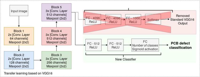
Following the standard transfer learning strategy [9], the top layers of the
pre-trained VGG16 [10] are removed, as shown in Figure 1. The new classifier
used consists of two fully connected layers of 512 units with ReLU activation and
0.3 dropout regularization [6]. The final classification layer has one sigmoid unit
for binary classification or six sigmoid units when used for multi-label classifi-
cation (one unit for each class). Moreover, we used the RMSProp optimization
algorithm with 10−5 learning rate and binary cross-entropy loss. Moreover we
also used online image data augmentation with geometric transformations as
vertical/horizontal flip and rotation [11].
Fig. 1: Transfer learning strategy based on VGG16 Model.
Regarding binary classification, two different input image sizes were used: the
default input size of the VGG16 (224x244) and the size of the images provided
by the DeepPCB dataset (640x640), further referenced by the full image size.
Based on [6] that found shallower models presented better accuracy in bi-
nary classification in the DeepPCB dataset, for each input size the following
experiments were performed for binary classification:
1. The classifier’s layers were connected after block 5 of the pre-trained model
VGG16, as shown in Figure 1, and the last two convolutional blocks (4 and
5) were fine-tuned;
2. The classifier’s layers were attached after block 4 of the VGG16 pre-trained
model, that is, block 5 was removed. Also, the two convolutional blocks
before classifier (blocks 4 and 3) were fine-tuned;
For multi-label classification, each one of the six output units is responsible for
classifying each defect type, working as multiple binary classifier with binary
cross-entropy loss. We used the best topology in binary classification experi-
ments to evaluate multi-label classification.
4 Experimental results
The experiments were done using the DeepPCB dataset [7], which has 3000
images, of those 1500 are template images (without defects) and 1500 are test
images (with one or more defects , Figure 2). Then we applied two methods: a
binary classification [6] and a multi-label classification problem [2].
657ESANN 2020 proceedings, European Symposium on Artificial Neural Networks, Computational Intelligence
and Machine Learning. Online event, 2-4 October 2020, i6doc.com publ., ISBN 978-2-87587-074-2.
Available from http://www.i6doc.com/en/.
(a) (b) (c) (d) (e) (f)
Fig. 2: Defect classes cropped from the DeepPCB dataset: (a) open, (b) short,
(c) mousebite, (d) spur, (e) copper and (f) pin-hole.
4.1 Results for binary classification
The results (mean of top 5 models) of accuracy and F1 score for the binary
classification on the DeepPCB dataset are showed in Table 1. The model with
all convolutional layers of pre-trained VGG16 (block 1 to block 5 in Figure 1)
and last two convolutional blocks fine tuned achieved 99.5% of accuracy on the
test set with 119,835,969 parameters (this model is referred as VGG16 block
5). It can be seen the decrease of the accuracy with the reduction of VGG16
convolutional layers, except when the input image size is 150x150.
Input size Metrics Models
VGG16 Block 5 VGG16 Block 4
Accuracy 83.6% 88.5%
150 x 150 F1 Score 0.811 0.879
(Results from [6]) Number of param. 19,172,673 29,132,609
Accuracy 95.8% 92.9%
224 x 224 F1 Score 0.958 0.928
Number of param. 27,823,425 59,279,169
Accuracy 99.5% 98.6%
640 x 640 F1 Score 0.995 0.984
Number of param. 119,835,969 427,329,345
Table 1: Results for binary classification for Fine Tuned models with different
size input images (input image size 150x150 were reproduced from [6]).
Since convolutional blocks followed by max pooling layer reduces the output
dimensions of network, less blocks implies in bigger feature maps to feed the fully
connected layers. The fully connected layers are responsible for most parame-
ters of VGGs based models. Because of this, for input image size of 640x640,
removing the block 5 of VGG16 increase the number of parameters in 3.57 times
(from 119,835,969 to 427,329,345 parameters).
From 1000 PCB images in test set, VGG16 block 5 model misclassified the
five images shown in Figure 3. For Figures 3 (a) and (b), the model reported a
false positive. The false positive for these particular images may be related to
the presence of numbers (3-087 can be seen in those images). Those numbers can
be confused as shorts, open or even cooper defects since it does not make part of
a regular circuit track. Exploring the training set we found sixteen examples of
PCB images containing text or numbers being six defective and ten not defective.
Figures 3 (c), (d) and (e) are false-negative errors. Figure 3 (c) has two short
658ESANN 2020 proceedings, European Symposium on Artificial Neural Networks, Computational Intelligence
and Machine Learning. Online event, 2-4 October 2020, i6doc.com publ., ISBN 978-2-87587-074-2.
Available from http://www.i6doc.com/en/.
(a) (b) (c) (d) (e)
Fig. 3: The five missclassified images by VGG16 block 5 model with full image
input size (frames were added to each image).
defects according to the corresponding annotation file. Those short circuits can
be visualized as the two non-uniform tracks in top right and top left. Even
for human inspection, shorts defects are hard to be found without a referential
image, because the short can also be part of a PCB project. The images from
Figure 3 (d) and (e) present more complex patterns to evaluate, although human
inspection can easily find an open-circuit defect in both images.
4.2 Results for multi-label classification
The individual results (mean of top 5 models) are showed in Table 2 with Accu-
racy and F1 score metrics. Besides that, the general results our non-referential
model are 0.952 of precision, 0.951 recall and 0.951 F1 score, while the best re-
sults found by Tang et al. using a referential approach are 0.982 precision, 0.981
recall and 0.982 F1 score, regarding that this approach requires the template im-
age for testing a PCB. Our proposed model achieved 95.1% of average accuracy
with the highest accuracy in open class (96.6%) and the lowest in mousebite
class (92.4%).
Exploring the DeepPCB dataset, defective images usually have multiple types
of irregularities. Only five examples have a single class and most of them have
at least three types of defect. This dataset characteristic causes some classes
being high correlated to other defects.
Class Open Short Mousebite Spur Cooper Pin Hole
Accuracy 96.6% 96.4% 92.4% 92.6% 96.4% 96.4%
F1 Score 0.966 0.964 0.924 0.926 0.964 0.964
Table 2: Results for each defect in multi-label classification.
5 Conclusion
The most recent advances in deep learning has brought attention to increase the
performance of automatic optical inspection for PCBs. We used a non-referential
approach based on transfer learning to evaluate if a PCB is defective (binary
classification) and which are the PCB defects (multi-label classification).
For binary classification we evaluated two input images sizes: the standard
VGG16 input size (224x224) and the default image size from the DeepPCB
dataset (640x640). We also evaluated different depth by removing convolutional
659ESANN 2020 proceedings, European Symposium on Artificial Neural Networks, Computational Intelligence
and Machine Learning. Online event, 2-4 October 2020, i6doc.com publ., ISBN 978-2-87587-074-2.
Available from http://www.i6doc.com/en/.
blocks of VGG16. We noticed the input image size as an import factor since
previous work reported 89% accuracy with input image of 150x150 pixels [6]. In
this work we used the full size input images and achieved an accuracy of 99.5%
with all convolutional blocks of pre-trained VGG16. It is worth mentioning that
increasing the input image size also increases the number of parameters of the
model, given that feature map extracted from convolutional layers increases as
well as showed in Table 1.
Regarding the multi-label classification, using the same structure of binary
classification model replacing only the final classification layer, the mean accu-
racy was 95.1% and the lowest accuracy achieved was 92.4% for the mousebite
defect. Using non-referential approach our model achieved neighbouring results
to the ones presented by Tang et al. with a referential approach. Since the
non-referential approach requires less information then the referential ones, our
model is very competitive in face of the solutions using referential approaches be-
cause it can overcome issues such as miss-alignment and illumination sensitivity
in a real production application.
References
[1] P. S. Malge and R. S. Nadaf. A Survey : Automated Visual PCB Inspection Algorithm.
International Journal of Engineering Research & Technology, 3(1):223–229, 2014.
[2] Linlin Zhang, Yongqing Jin, Xuesong Yang, Xia Li, Xiaodong Duan, Yuan Sun, and Hong
Liu. Convolutional neural network-based multi-label classification of PCB defects. The
Journal of Engineering, 2018(16):1612–1616, 2018.
[3] Barnajit Ghosh, M. K. Bhuyan, Pradipta Sasmal, Yuji Iwahori, and Prathik Gadde.
Defect Classification of Printed Circuit Boards based on Transfer Learning. In 2018 IEEE
Applied Signal Processing Conference (ASPCON), pages 245–248. IEEE, dec 2018.
[4] A.M. Darwish and A.K. Jain. A rule based approach for visual pattern inspection. IEEE
Transactions on Pattern Analysis and Machine Intelligence, 10(1):56–68, 1988.
[5] Yohei Takada, Tokiko Shiina, Hiroyasu Usami, and Yuji Iwahori. Defect Detection and
Classification of Electronic Circuit Boards Using Keypoint Extraction and CNN Features.
The Ninth International Conferences on Pervasive Patterns and Applications Defect
2017, (c):113–116, 2017.
[6] Leandro H De S Silva, George O. de A. Azevedo, Bruno J. T. Fernandes, Byron L. D.
Bezerra, Estanislau B. Lima, and Sergio C. Oliveira. Automatic Optical Inspection for
Defective PCB Detection Using Transfer Learning. In 2019 IEEE Latin American Con-
ference on Computational Intelligence (LA-CCI), Guayaquil, 2019.
[7] Sanli Tang, Fan He, Xiaolin Huang, and Jie Yang. Online PCB Defect Detector On A
New PCB Defect Dataset. page 5, feb 2019.
[8] Karl Weiss, Taghi M. Khoshgoftaar, and DingDing Wang. A survey of transfer learning.
Journal of Big Data, 3(1):9, dec 2016.
[9] Jason Yosinski, Jeff Clune, Yoshua Bengio, and Hod Lipson. How transferable are features
in deep neural networks? 27, nov 2014.
[10] Karen Simonyan and Andrew Zisserman. Very Deep Convolutional Networks for
Large-Scale Image Recognition. pages 1–14, sep 2014.
[11] Connor Shorten and Taghi M. Khoshgoftaar. A survey on Image Data Augmentation for
Deep Learning. Journal of Big Data, 6(1):60, dec 2019.
660You can also read