CUIN1-XGAXSE2 SOLAR CELLS - MASTER IN INGEGNERIA DEL FOTOVOLTAICO CORSO DI TECNOLOGIE FOTOVOLTAICHE CONVENZIONALI FRANCESCO BICCARI ...
←
→
Page content transcription
If your browser does not render page correctly, please read the page content below
CuIn1-xGaxSe2 solar cells

        Master in Ingegneria del Fotovoltaico
   Corso di Tecnologie Fotovoltaiche Convenzionali

                 Francesco Biccari
                 biccari@gmail.com

                    2012-04-25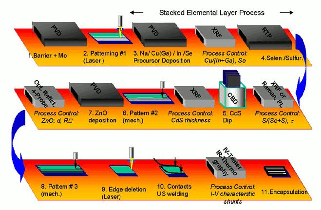
Chalcopyrite semiconductors
     The term chalcopyrite refers to the crystal structure of several
     chalcogenides (chalcogen (element of group 16) + electropositive
     elements).
     In common language chalcopyrite is
     identified with CuFeS2, the first discovered
     compound with this structure.
     In photovoltaic community chalcopyrite
     indicates in particular 4 compounds:

   Chalcopyrite                  a (Å)       c (Å)      Eg (eV)        ηth (%)        ηexp (%)

   CuInSe2 (CISe)                5.78       11.62         1.04            31            15.4

   CuInS2 (CIS)                  5.52       11.08         1.57            31            12.3

   CuGaSe2 (CGSe)                5.61       11.01         1.68            28             9.5

   CuGaS2 (CGS)                  5.35       10.48         2.43            12              –
                                                                                                           d(Se-Cu) ≠ d(Se-In)
                                                                                                               Source: Wikipedia
Francesco Biccari – Master Ingegneria del Fotovoltaico – Corso di Tecnologie Fotovoltaiche Convenzionali                           2/47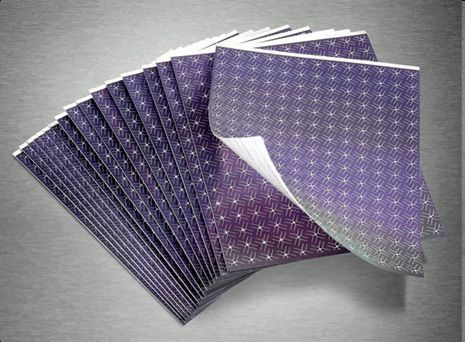
Electronic and optical properties
   • All these compounds are naturally p type because of the
     presence of copper vacancies VCu which behave as
     acceptors

   •    CISe: Χ = 4.6 eV, me = 0.09 m0, εr = 13.6
   •    CGSe: Χ = 4.0 eV, me = 0.14 m0, εr = 11.0
   •    CIS: ?
   •    CGS: ?
   •    Good electron effective mass!

   • Direct gap and one of the highest absorbtion coefficient!
Francesco Biccari – Master Ingegneria del Fotovoltaico – Corso di Tecnologie Fotovoltaiche Convenzionali   3/47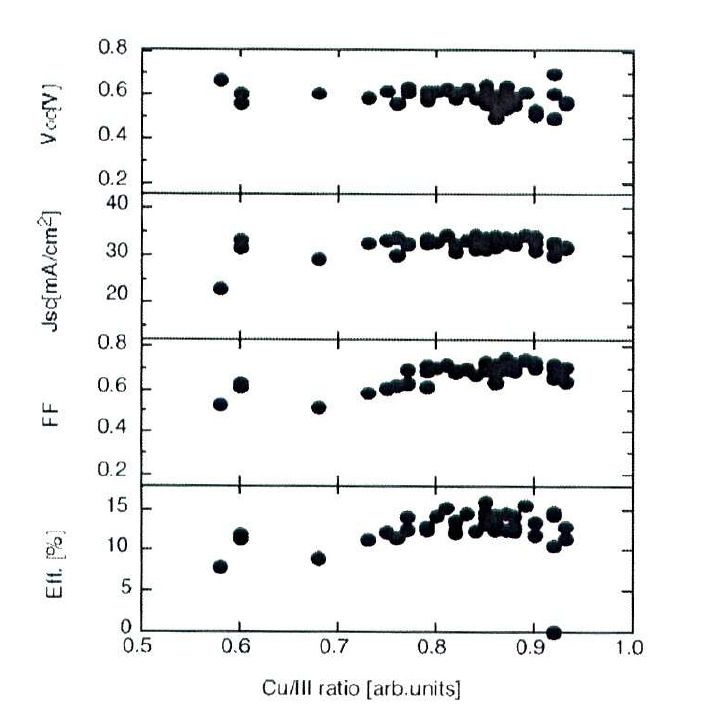
The n-type doping problem in CGSe
     CISe can be grown both n and p type!
     CGSe can be obtained p type only. Explanation (ab-initio calculations):

    Critical EF value at which the VCu formation energy becomes zero. VCu are acceptors!
                                                                 Zhao Y., Persson C., Lany S., Zunger A. Appl. Phys. Lett., 85, 5860,
                                                                 (2004)
Francesco Biccari – Master Ingegneria del Fotovoltaico – Corso di Tecnologie Fotovoltaiche Convenzionali                            4/47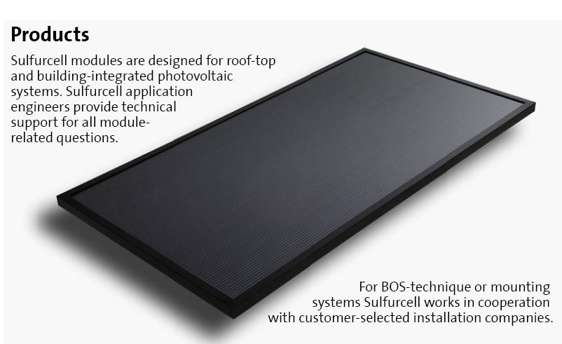
CISe: stoichiometry variations
  Ternary Cu-In-S
  phase diagram at
  500°C.

  The most relevant
  phases lie on the
  quasi-binary                                    In2Se3
  intersection:
  Cu2Se-In2Se3.

                                                                                                           Cu2Se

Francesco Biccari – Master Ingegneria del Fotovoltaico – Corso di Tecnologie Fotovoltaiche Convenzionali           5/47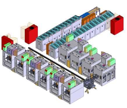
CISe: stoichiometry variations

                          [Cu]/[In]=0.66                                 The cell efficiency change only slightly if:
  CIGS has a good tolerance to                                                   0.8< [Cu]/([In]+[Ga])0.95
  0.95 to 0.82
Francesco Biccari – Master Ingegneria del Fotovoltaico – Corso di Tecnologie Fotovoltaiche Convenzionali           6/47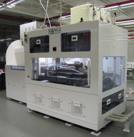
Chalcopyrites solar cells. Brief history
   1953. Hahn. Synthesis and characterization of CISe
   1974. First single crystal CISe/CdS solar cell at Bell Labs
   1975. CISe/CdS 11% at Bell Labs
   1976. Univ. of Maine. First polycrystal CISe/CdS and CIS/CdS solar cells
   1977. Univ. of Maine. First p-n CISe homojunction. 3%
   1981. Boeing company obtains polycrystalline CISe/CdS 11.4% (coev.)
   1980’s. Single crystals are abandoned in favor of thin films.
                Boeing (coevaporation) vs ARCO (selenization)
   1986. Thick CdS abandoned. Thin CdS + thick doped ZnO
   1987. Gallium alloying. Born of CIGSe
   1993. The positive effect of sodium is discovered (soda lime glass) and the Ga
             gradient is introduced.
   1998. NREL CIGSe/CdS 19% on glass. 2008. EMPA 17.4% on polyimide
Francesco Biccari – Master Ingegneria del Fotovoltaico – Corso di Tecnologie Fotovoltaiche Convenzionali   7/47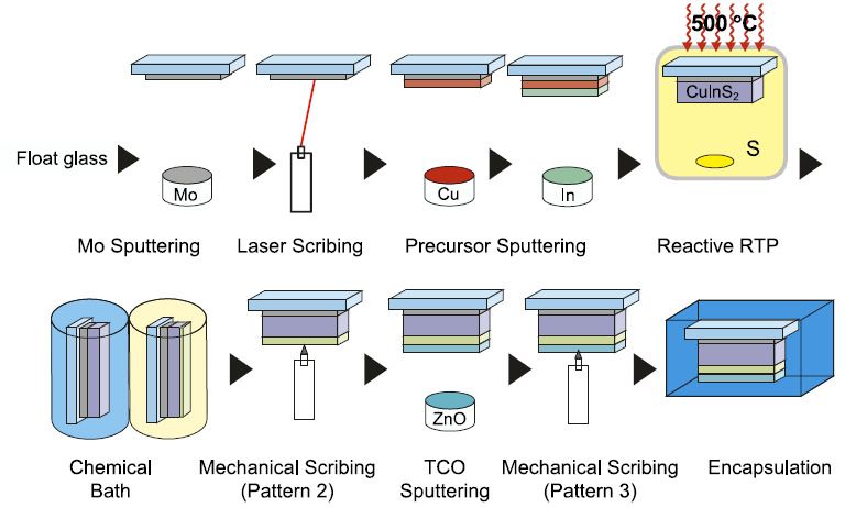
CIGSe and CIGS alloys
   • CISe pn homojunction have poor efficiency! (Why?)

   • The lattice parameters of chalcopyrites are similar. I can make
     alloys in order to increase Voc.              Why the Voc increases
                                                                                                           with the band gap?

   • Using alloys CuIn1-xGaxSe2 (CIGSe) with Ga content between
     25% and 30% they reached 20.3% efficiency
   • Using alloys CuIn1-xGaxS2 (CIGS) with Ga content of 10% they
     reached good efficiency

   • For larger Ga fractions the photovoltage saturates leading to a
     decrease of conversion efficiencies.

Francesco Biccari – Master Ingegneria del Fotovoltaico – Corso di Tecnologie Fotovoltaiche Convenzionali                        8/47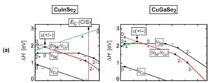
CIGSe alloy
                                                                Ga/(Ga+In)
                                                        0.3         0.6            0.9

                                      18
                     Efficiency (%)

                                      16

                                      14                                                       The Voc does not increase
                                      12
                                                                                               linearly with Eg!
                                      10

                                            1.0   1.1     1.2   1.3    1.4   1.5   1.6
                                                                                               Usually CIGSe refers to the
                                                                                               composition
  Open Circuit voltage (V)

                                      0.9
                                                                                               CuIn1-xGaxSe2 with x = 0.3
                                      0.8

                                      0.7                                                      CuIn0.7Ga0.3Se2
                                      0.6                                                      Eg = 1.15 eV
                                      0.5
                                            1.0   1.1     1.2   1.3    1.4   1.5   1.6   1.7
                                                        Absorber band gap (eV)

Francesco Biccari – Master Ingegneria del Fotovoltaico – Corso di Tecnologie Fotovoltaiche Convenzionali                     9/47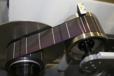
Explanation of the Voc saturation

  If the CIGSe, like pure CGSe, is able to equilibrate at the temperatures used during
  the junction formation it will react to the EF upward shift creating a large amount of
  VCu (acceptor defects). This effect will reduce the band bending in the absorber, it will
  introduce a large interface recombination and therefore it will give a lower Voc.

Francesco Biccari – Master Ingegneria del Fotovoltaico – Corso di Tecnologie Fotovoltaiche Convenzionali   10/47
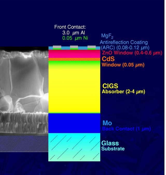
CIGSe solar cell structure

                    Substrate configuration                                   Superstrate configuration
                  Need an encapsulating glass                         No transparent encapsulation on the back!
                  Max eff 20%. Currently used                         Max eff 12.8% (Cd diffusion). Abandoned
                                                                                       Source: Poortmans (2006)

Francesco Biccari – Master Ingegneria del Fotovoltaico – Corso di Tecnologie Fotovoltaiche Convenzionali          11/47
CIGSe solar cell structure
Substrate
configuration
Francesco Biccari – Master Ingegneria del Fotovoltaico – Corso di Tecnologie Fotovoltaiche Convenzionali 12/47Back contact
• The work function of CIGSe is 4.6 eV. A metal with an high work function is
needed. Mo has a work function of 4.6 eV, insufficient, in principle.
?
• However Mo back contact seems to be ohmic (with strange I-V)!
• Explanation: MoSe2? This layer is formed during CIGSe deposition.
Tunnelling? Variable Mo work function?
• Back contact is usually made of molybdenum and deposited by DC
sputtering
• Important role of MoSe2 (adhesion)
Francesco Biccari – Master Ingegneria del Fotovoltaico – Corso di Tecnologie Fotovoltaiche Convenzionali 13/47Features of CIGSe growth
• Copper. We need a deficiency of
copper (p type). But Cu excess: grain
growth, less defect concentration,
CuxSe segregation.
In Cu deficiency the best cell has 14%
of efficiency.
Several process were developed to
use the good impact of Cu excess.
SIMS Profile for Na
• Sodium. Diffuse from (soda lime) glass
trough the Mo grain boundaries. Better
morphology, p-type doping (Voc, FF). It
can be put in definite quantities with a
blocking layer and NaF deposition.
Or by a soda lime thin film on flexible
substrates
Francesco Biccari – Master Ingegneria del Fotovoltaico – Corso di Tecnologie Fotovoltaiche Convenzionali 14/47Features of CIGSe growth
• Gallium. In the highest-efficiency cells, the gallium content
increases from 5–8% near the front junction to about 10–15%
at the back contact, while the indium content correspondingly
decreases toward the back.
This composition gradient yields an increasing conduction
band energy that produces a driving force to aid collection of
electrons (minority carriers in the p-CIGS) by the n-CdS.
These composition gradients act similarly to the “back surface
field” in the silicon structure.
Gallium enhances the MoSe2 formation on the back contact
Francesco Biccari – Master Ingegneria del Fotovoltaico – Corso di Tecnologie Fotovoltaiche Convenzionali 15/47Deposition of CIGSe
• Co-evaporation or co-sputtering of elements on heated substrate. Se in excess. (best
composition control, graded composition, CuxSe aid)
– Bilayer process (Boeing)
– Inverted bilayer process
– Three stage process (the best process! Eff. record)
• Evaporation or sputtering of Cu, Ga, In and subsequent reaction in H2Se atmosphere
or Se atmosphere (selenization) in tube furnace or RTP.
• Nanoparticle “inks” (or “paints”) that are applied using non-vacuum coating
techniques and then reacted into semiconductor films
• Electrodeposition and subsequent selenization/sulfurization
• From liquid phase, η = 10.3%
(D. B. Mitzi. Solution processing of inorganic materials. Wiley-Interscience (2009))
• CVD
Francesco Biccari – Master Ingegneria del Fotovoltaico – Corso di Tecnologie Fotovoltaiche Convenzionali 16/47Deposition of CIGSe. Co-evaporation
Bi-layer process (Boeing)
It starts with the deposition of Cu-rich Cu(In,Ga)Se2 (grain growth) and ends with an
excess In rate (no extra phases).
Inverted process
Deposition without copper of (In,Ga)2Se3 (likewise In,Ga, and Se from elemental
sources to form that compound) at low temperatures (typically around 300°C).
Then, Cu and Se are evaporated at an elevated temperature (550°C) until an overall
composition close to stoichiometry is reached. This process leads to a smoother film
morphology when compared to the bi-layer process. Some CuxSe remains.
Three-stage process
Deposition of In, Ga, and Se at the end of an inverted process to ensure the overall In-
rich composition of the film even if the material had been Cu-rich during the second
stage (grain growth, no extra phases).
This process allows also to introduce Ga gradients into the absorber and thus enables
us to design a graded band-gap structure (Ga gradient).
During the third stage it is possible to detect Cu-rich and Cu-poor condition from a
change in the thermal properties or optical properties
Francesco Biccari – Master Ingegneria del Fotovoltaico – Corso di Tecnologie Fotovoltaiche Convenzionali 17/47Deposition of CIGSe. Co-evaporation
A. Romeo et al. Progress in photovoltaics, 12, 93 (2004)
Francesco Biccari – Master Ingegneria del Fotovoltaico – Corso di Tecnologie Fotovoltaiche Convenzionali 18/47Deposition of CIGSe. Co-evaporation
Example of bilayer industrial process (Boeing)
Source: Poortmans (2006)
Francesco Biccari – Master Ingegneria del Fotovoltaico – Corso di Tecnologie Fotovoltaiche Convenzionali 19/47Deposition of CIGSe. Co-evaporation Example of three-stage industrial process: Würth Solar. Other companies: Global Solar, Ascent Solar, Solibro. Francesco Biccari – Master Ingegneria del Fotovoltaico – Corso di Tecnologie Fotovoltaiche Convenzionali 20/47
Deposition of CIGSe. Selenization
   • More industrial troughput. Difficult optimization due to the
     importance of kinetics of several reactions

   • Solar Frontier (ex Showa Shell) does not use CdS!
     Annealing in H2S. η = 11%
   • Shell Solar (Avancis) use CdS by CVD. η = 9%
   • Miasolé. Unknown process. η = 9%
   • Energy Photovoltaics (EPV). Hybrid process (coevaporation for In
     and Ga in Se atmopshere, sputtering of Cu, selenization). Low
     defect concentration!
Francesco Biccari – Master Ingegneria del Fotovoltaico – Corso di Tecnologie Fotovoltaiche Convenzionali   21/47
CdS
CdS is a semiconductor with
CdS
Eg = 2.42 eV. It is yellow! ZnO
It should be a window layer but it should CIGSe
be as thin as possible (we will see why)
and it is called buffer layer.
Mo
Deposition methods: Glass, Metal foil,
plastics
Evaporation
Sputtering
Close Spaced Sublimation (CSS)
Vapour Transient Deposition (VTD)
Chemical Vapour Deposition (CVD)
Chemical Bath Deposition (CBD)
Francesco Biccari – Master Ingegneria del Fotovoltaico – Corso di Tecnologie Fotovoltaiche Convenzionali 22/47CdS
• Compact to reduce shunts
• It can suffer from the subsequent processes (usually in superstrate configuration)
• Lattice mismatch with the absorber: defects
• Ordered Vacancy Compound
(OVC) near the interface!
CuIn3xGa3(1-x)Se5
• Cd donor dopant? Poortmans
• Partecipation to carrier
collection?
• High absorption in blue:
usage of ZnO as window layer.
CdS very thin!
• High resistance: usage of AZO
as window layer. CdS very thin!
• Protection of the absorber against
sputter damage during AZO
window deposition
Francesco Biccari – Master Ingegneria del Fotovoltaico – Corso di Tecnologie Fotovoltaiche Convenzionali 23/47CdS deposited by CBD
• Best results are obtained by
Chemical Bath deposition (CBD)
• Solution:
Cd2+ source (CdSO4, CdI2) + NH3 + S2- source (thiourea)
+ H 2O
T = 70°C
• Reaction of Cd2+ with S2- to form CdS
Francesco Biccari – Master Ingegneria del Fotovoltaico – Corso di Tecnologie Fotovoltaiche Convenzionali 24/47R&D automated setup for CBD
Intermediary
transport unit
Final
Pre Rinse
Rinse
Side channel
blower
Dosage
Unit
Temp. Control
Stand alone
modules
Robot
Handling
Francesco Biccari – Master Ingegneria del Fotovoltaico – Corso di Tecnologie Fotovoltaiche Convenzionali 25/47CdS alternatives CdS is usually thicker than necessary in industrial process: high absorption in blue region. The buffer could be changed from CdS (Eg = 2.42 eV) to ZnS (Eg = 3.7 eV) or In2S3:Na (Eg = 2.2 ÷ 2.95 eV) to improve carrier collection in the blue. Francesco Biccari – Master Ingegneria del Fotovoltaico – Corso di Tecnologie Fotovoltaiche Convenzionali 26/47
CIGSe solar cells. TCO
   • The cell is completed with two layers of ZnO:
      – A first thin layer 100 nm of intrinsic ZnO useful for reducing pin holes
      – A thick 400 nm layer of AZO (aluminium doped ZnO)

   • ZnO and AZO are
     deposited by RF sputtering
     at relatively low temperature
     (150°C or less) to avoid Cd
     diffusion in CIGSe

   • The best resistivity of AZO
     is 5 x 10⁻⁴ Ω cm (higher
     doping reduces the mobility                                                                           Poortmans
     and increases the free
     carrier absorption).

   • Alternatives: BZO
     (high mobility)

Francesco Biccari – Master Ingegneria del Fotovoltaico – Corso di Tecnologie Fotovoltaiche Convenzionali          27/47
CIGSe modules
• Laser or mechanical scribing to create stripes connected
in series
• Encapsulation with EVA
Poortmans
Francesco Biccari – Master Ingegneria del Fotovoltaico – Corso di Tecnologie Fotovoltaiche Convenzionali 28/47CIGSe commercial modules Manufacturing capacity: Solar Frontier (Showa Shell company) (Japan): 900 MW in 2012! Global Solar (USA) 140 MW (roll to roll) 10% efficiency Avancis (Germany) (15.5% on 30 cm x 30 cm module!) Würth Solar (Germany) 30 MW Ascent Solar (USA): 1.5 MW (8% on plastic) 12% efficiency Francesco Biccari – Master Ingegneria del Fotovoltaico – Corso di Tecnologie Fotovoltaiche Convenzionali 29/47
CIGSe commercial modules
   Manufacturing capacity:
   Solibro (Q-Cells company) (Germany): 13% efficiency!

   Solyndra (USA)

   Heliovolt (USA)
   12 % efficiency

   Solarion (Germany)
   13% (?) roll to roll on plastic
   and rigid modules

Francesco Biccari – Master Ingegneria del Fotovoltaico – Corso di Tecnologie Fotovoltaiche Convenzionali   30/47
Avancis process
  • SiNx barrier before Mo layer

  • Sodium dopant by DC
  sputtering

  • Alternate layers Cu (85%) +
  Ga (15%) and In

  • Thermally evaporated Se
  layer

  • Selenization in RTP (IR
  lamps) 10°C/s! The chamber
  has a minimized volume to
  ensure high pressure of Se
  and S. S is introduced by an
  additional gas feed.
                                                                          Time resolved photoluminesce
  The process has probably a                                              and other advanced techniques
  duration of about 10 minutes.                                           for quality control!

Francesco Biccari – Master Ingegneria del Fotovoltaico – Corso di Tecnologie Fotovoltaiche Convenzionali   31/47
Centrotherm turnkey line
Process: precursor/selenization
Cost: 60 M€ for a capacity of 50 MW/y
First module produced in January
2010 in a line installed in Taiwan
Module eff. 12%, 170 Wp
Francesco Biccari – Master Ingegneria del Fotovoltaico – Corso di Tecnologie Fotovoltaiche Convenzionali 32/47Flexible CIGS Modules: Nanosolar
• Aluminium foil + Mo
• CIGSe printed with ink
containing nanoparticles + RTP
Founded in 2002
Production capacity = 430 MW
Production 2009 = 4 MW
Eff.: 11.6% module, 15.3% cell
• Wrap-Through back contact
on a second aluminium foil
Francesco Biccari – Master Ingegneria del Fotovoltaico – Corso di Tecnologie Fotovoltaiche Convenzionali 33/47CIGSe solar cells stability
Adverse effect of humidity on unprotected ZnO: degradation was
shown to come from a resistivity increase but this drawback was
overcome with proper encapsulation.
No formation of Cu2S at the interface between CdS and In-
rich CIS.
Cd in-diffusion is kinetically limited and poses no threat to
the interface stability (D(Cd in CIS) = 10-19 cm2/s at room ZnO
temperature).
CIGSe
Mo/CIGS interface: very stable with no evidence of Mo
diffusion into the CIGS film. An interfacial MoSe2 layer of a Mo
10 nm thickness can be formed. This layer is possibly
beneficial in producing an ohmic back contact at room Glass, Metal foil,
temperature. plastics
Francesco Biccari – Master Ingegneria del Fotovoltaico – Corso di Tecnologie Fotovoltaiche Convenzionali 34/47CIGSe solar cells stability
Why Cu outdiffusion is very likely in Cu2S/CdS cells but highly unlikely in
CIGSe/CdS cells?
1. µCu(Cu2S) > µCu(CdS) 1. µCu(CIS) < µCu(CdS)
2. The electric potential drop 2. The electric potential drop
across the Cu2S/CdS interface is across the CIS/CdS interface is
small, so that under forward bias high, so that even under forward
an overpotential results in a bias Cu outdiffusion is very unlikely
driving force for Cu outdiffusion
Francesco Biccari – Master Ingegneria del Fotovoltaico – Corso di Tecnologie Fotovoltaiche Convenzionali 35/47CIGSe solar cells stability
Test solar frontier
Test Global Solar
S. Wiedeman, TFPP 2006
Francesco Biccari – Master Ingegneria del Fotovoltaico – Corso di Tecnologie Fotovoltaiche Convenzionali 36/47CIS solar cells
• Sulfurcell in Germany has developed a manufacturing
process for this cell technology
• Using Cu-rich CIS thin films efficiencies of over 12%
have been achieved. No sodium needed! However the
CuxS phase has to be removed in a further step which
can easily be done by KCN treatment. A solution is the
usage of Cu-poor film with Na doping.
• Eg greater than in CIGSe: smaller temperature
coefficient
Francesco Biccari – Master Ingegneria del Fotovoltaico – Corso di Tecnologie Fotovoltaiche Convenzionali 37/47CIS solar cells. Development
• Voc improvement
– Ga alloying of CIS (larger
concentration in the back of the
cell)
– Lower electron affinity buffer
layer. n-CdS is considerably
less appropriate for CIS
because the electron affinities
between the materials differ by
about 0.4 eV, thus limiting the
contact potential difference and
thus the achievable Voc
• jsc improvement
– Larger Eg window layer
(i.e. Zn(S,O))
Francesco Biccari – Master Ingegneria del Fotovoltaico – Corso di Tecnologie Fotovoltaiche Convenzionali 38/47CIS solar cells. Sulfurcell process Sulfurization of precursors in RTP furnace. Only 5 minutes in RTP!!! Max eff. 8.6% Francesco Biccari – Master Ingegneria del Fotovoltaico – Corso di Tecnologie Fotovoltaiche Convenzionali 39/47
CIGSe and others. Production
                        CIGS                                               2009 MW/yr                         2010 MW/yr
                                                                       Capacity Production                 Capacity Production
  Solar Frontier (Showa Shell)                       JPN                       80                45             80         80
  Solibro (Q-cells)                                  DEU                       30                20            135         95
  Solindra                                           USA                     110                 30              -           -
  Wurth Solar                                        DEU                       30                30             40         40
  Global Solar                                   USA+DEU                       75                20             75         55
  Avancis (Shell+Saint Gobain)                       DEU                       20                 5             20         20
  Sulfurcell                                         DEU                         3                2             35         18
  Nanosolar                                          USA                     430                  4            430           -

  2009 total production:                           210 MWp
  2010 total production:                           435 MWp
Francesco Biccari – Master Ingegneria del Fotovoltaico – Corso di Tecnologie Fotovoltaiche Convenzionali                     40/47
Materials availability: a future problem?
Indium requirement: 0.03 g/Wp: the
price is still acceptable
The entire In production would give a
maximum of 10 GWp/yr PV production.
J.J. Scragg et al, Phys. stat. sol. (b) 245, 1772 (2008)
Francesco Biccari – Master Ingegneria del Fotovoltaico – Corso di Tecnologie Fotovoltaiche Convenzionali 41/47Materials availability: a future problem?
Source: B. A. Andersson , Prog. Photovolt. Res. Appl. 8, 61 (2000)
Metal Reserves Production Limit 1999 limit 2020 limit
Modules
Required 1998 1999 power annual prod annual prod
(Eff≈10%)
(g/m2) (Gg) (Gg/yr) (TWp) (GWp/yr) (GWp/yr)
CdTe (2 µm) Cd 6.3 600 20
Te 6.5 20 0.29 0.3 5 20
CIGS (2 µm) Se 4.8 70 2.2
Ga 0.53 110 0.054
In 2.9 2.6 0.29 0.09 7 70
aSiGe (0.2 µm) Ge 0.44 2 0.063 0.5 14 200
Dye Ru 0.1 6 0.011 6 11 20
Total PV 2010 production ≈ 27 GWp (2 GWp due to CdTe and CIGS)
No availability problems in the next 5-10 years
On the long term availability problems for In and Te could arise.
(105 TWh 2006 world consumption: 10 TWp of PV)
Francesco Biccari – Master Ingegneria del Fotovoltaico – Corso di Tecnologie Fotovoltaiche Convenzionali 42/47Grain boundaries role in CIGSe
“Why are polycrystalline thin-film PV
devices more efficient than their
single crystal counterparts?”
Maybe the grain boundaries in the
columnar grains act as preferential
minority carrier paths (barrier for
holes and well for electrons)
Francesco Biccari – Master Ingegneria del Fotovoltaico – Corso di Tecnologie Fotovoltaiche Convenzionali 43/47Minority carrier lifetimes in CIGSe
Time resolved photoluminescence
2 ns < τn < 200 ns.
If µn = 100 cm2/(Vs) and τn = 10 ns then Ln=1.6 µm
kT
Ln = Dτ n = µ n τn
q
This is partly confirmed by direct EBIC
measurements
Fast τn decrease in air! B. Ohnesorge et al. Appl. Phys. Lett., 73, 1224
(1998)
Francesco Biccari – Master Ingegneria del Fotovoltaico – Corso di Tecnologie Fotovoltaiche Convenzionali 44/47CIGS solar cells. Conclusions (1)
• High efficiency
– The polycrystalline nature of the thin film is not detrimental and poly thin film
solar cells give higher efficiency compared to their single crystal counterparts
• Stability
– The large stoichiometry variations (a few percents) and defect density are not
detrimental
– Impurities in large concentrations (i.e. Fe at 1017 cm-3) do not cause any
performance degradation or stability problem and in the case of Na (at 1020
cm-3) a performance improvement is observed.
• Low cost
– Effective use of raw materials
– Small energy pay-back time (less than two years)
– No doping: the p-type conductivity due to intrinsic defects is used
• Adaptable to various applications
• Large supporting research and development community
Francesco Biccari – Master Ingegneria del Fotovoltaico – Corso di Tecnologie Fotovoltaiche Convenzionali 45/47CIGS solar cells. Conclusions (2)
• CIGSe modules have reached 431 MWp of production in 2010
• CIGSe has the highest efficiencies and potentialities, but also the highest
cost with respect to CdTe and a-Si.
• At the moment the main product type is a glass monolithic module but
probably a large production increase will derive from the introduction of
flexible modules.
• A few companies are starting to deliver turnkey production lines.
• Materials availability is not going to be a big problem in the next years and it
will improve in response to demand and price increase.
• Environmental and safety problems are manageable in the production phase
and almost irrelevant for the user.
Francesco Biccari – Master Ingegneria del Fotovoltaico – Corso di Tecnologie Fotovoltaiche Convenzionali 46/47Acknowledgments
• Thanks to Dr. Alberto Mittiga for providing several
figures, numbers and slides of this presentation
• Thanks to Dr. Rosa Chierchia for useful discussions
Francesco Biccari – Master Ingegneria del Fotovoltaico – Corso di Tecnologie Fotovoltaiche Convenzionali 47/47You can also read