Data Retention Fault in SRAM Memories: Analysis and Detection Procedures
←
→
Page content transcription
If your browser does not render page correctly, please read the page content below
Data Retention Fault in SRAM Memories:
                                                                   *
                                 Analysis and Detection Procedures

           Luigi Dilillo          Patrick Girard           Serge Pravossoudovitch            Arnaud Virazel
               Laboratoire d’Informatique, de Robotique et de Microélectronique de Montpellier – LIRMM
                                          Université de Montpellier II / CNRS
                                   161, rue Ada – 34392 Montpellier Cedex 5, France
                          Email: @lirmm.fr URL: http://www.lirmm.fr/~w3mic

                                             Magali Bastian Hage-Hassan
                                              Infineon Technologies France
                                 2600, Route des Crêtes – 06560 Sophia-Antipolis, France
                                          Emails: magali.bastian@infineon.com
                                             URL: http://www.infineon.com

                        Abstract*                               dense, and their capacity grows at the same time.
                                                                Consequently, these devices are more prone to faults and
   In this paper, we present a novel study on Data              testing them efficiently becomes very important for the
Retention Faults (DRFs) in SRAM memories. We analyze            yield of SoCs.
in detail the electrical origins of these faults, starting        The functional fault models traditionally employed in
from the most common till those that lead to what we            SRAM testing are nowadays insufficient to test the
have called hard to detect DRFs. In general, DRFs are           effects produced by some defects that may occur in
supposed to be produced by very high resistive-open             VDSM technologies. Improvements in manufacturing
defects that affect the refreshment loop of the core-cell.      process quality and memory architecture have lead to the
We demonstrate that lower values of resistance may              development of new fault models, which are tightly
produce hard to detect DRFs. Moreover, each resistive-          linked to the internal memory structure. These faults need
open defect produces a particular faulty behavior of the        specific test solutions. Moreover, the presence of
core-cell that changes for different ranges of the resistive    resistive-open defects is becoming more and more
value. We analyze different cases and we propose for            important, due to the ever-growing number of
each one an efficient test procedure based on March             interconnections between the layers. In particular, it is
tests. In particular, we propose to stimulate the defective     reported in [Need98] that open/resistive vias are the most
cells in some cases by indirect accesses and in some other      common root cause of test escapes in deep-submicron
cases by emphasizing natural noise phenomenon of                technologies.
SRAM memories (such as the ground bounce).
                                                                  Several studies on the influence of resistive-open
                                                                defects on the correct operation of SRAM core-cells have
                                                                been published recently [2,3,4]. In this paper, we consider
1. Introduction                                                 resistive-open defects that, occurring in the refreshment
                                                                loop, may cause data retention faults (DRFs). The
  In modern integrated circuits such as System-on-Chip
                                                                proposed analyses concern the different forms of DRF in
(SoC) the importance of memories is growing. Actually,
                                                                correlation with the location of the defect and its resistive
the ITRS roadmap [1] forecast that in 2013 over 90% of
                                                                value.
the SoC area will be taken by memories, in particular
embedded-SRAMs. The SRAMs are more and more                       The rest of the paper is organized as follows. In Section
                                                                2, we describe in detail the state of the art of the
                                                                electrical origins and the test solutions for the DRF. In
*
 This work has been partially funded by the French government   Section 3, we expose the analyses of the hard to detect
under the framework of the MEDEA+ A503 "ASSOCIATE"              DRFs and we propose algorithmic procedures useful for
European program.                                               their test. In particular we identify two sub-cases of hard

                                                            2
to detect DRFs and we propose to produce their floating high, because the pull-up of INV2 does not work
sensitization by stimulating the defective cells by indirect correctly due to defect Df1. In this conditions, if the
accesses and by emphasizing a natural noise phenomenon natural leakage currents that discharge node SB
of SRAM memories such as the ground bounce. (especially through Mtn1 and Mtn4) are higher than the
Conclusions and perspectives are given in Section 4. current that passes through the faulty pull-up of INV1 the
voltage value of node SB slowly decreases from Vdd to
2. Data Retention Faults: the state of the art Vdd/2. When node SB is under the threshold value of
Vdd/2, INV2 switches, immediately followed by the
The definition of Data Retention Fault (DRF) is the switch of INV1, so that a faulty swap of the cell occurs
following: with the loss of the stored information.
A DRF occurs when a memory cell loses its previously We have simulated this phenomenon on the Infineon
stored logic value after a certain period of time during 0.13 µm embedded SRAM, in particular on a cell in
which it has not been accessed [5]. which we have inserted the resistive-open defect Df1
In general this kind of fault is the consequence of with the following parameters:
resistive-open defects in SRAM core-cells, in particular - Process: fast
in the self-refreshment loop circuit. Figure 1 depicts the - Supply voltage: 1.6 V
scheme of a standard six transistors core cell in which we
have inserted three resistive-open defects in locations - Temperature: 120°C
where they are commonly the cause of DRFs [5, 6]. - Resistive-open defect: Df1 = 100 MΩ
These defects are denoted as Df1, Df2 and Df3. The evolution of the phenomenon of DRF, described
BL
WL
BLB above, is clearly reproduced on the waveforms in Figure
Vdd
2.
Df1
INV1 Mtp1
Df3
SB
Mtn1
Mtn3 S Vdd Mtn4
Df2 Core-cell
INV2 SB swap
Mtp2
Mtn2
S
Figure 1: Resistive-open defects injected
into the memory core-cell as cause of DRFs.
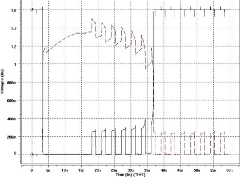
In order to explain the mechanism of DRFs we consider w0 No access
a core-cell with a resistive-open defect in the pull-up of
the inverter INV1; this defect corresponds to Df1 that Figure 2: Data retention fault caused by high resistive
restrains the current flow between Vdd and node SB. In defect Df1
[2] we have demonstrated that this defect may cause
Read Destructive Faults (RDFs), or dynamic Read We can observe that just after the w0 operation node S
Destructive Faults (dRDFs), in certain range of resistive is at ‘0’, while node SB is at ‘1’, but with a level lower
value. When Df1 has a very high resistive value, larger than Vdd due to the faulty pull-up of INV1. For the same
than 100 MΩ, it behaves like a quite pure open circuit reason node SB slowly loses the stored charge because of
and involves DRFs. the leakage currents. With the decrease of the voltage of
When a ‘0’ is stored in the cell, bit line BL discharges node SB also INV2 begins to work not perfectly, in
node S to ‘0’, while BLB charges node SB to ‘1’. At the particular Mtn2 conducts less than normal and Mtp2
end of the w0 operation the two pass-transistor Mtn3 and starts to conduct. Consequently the voltage of node S
Mtn4 are off and the cell is isolated from the bit lines. At grows slowly. When node SB reaches the threshold of
this moment node S is active low due to the pull-down of Vdd/2, INV2 switches and the cell swaps.
the inverter INV2 (see Figure 1), while node SB is
3In this experiment, the resistive value of defect Df1 appear, but the behavior of the faulty cell is more
(100 MΩ) is enough to produce a DRF. Generally the complex. In these circumstances the DRFs are hard to
value of Df1 has to be much higher. Here, the particular detect. This case is discussed in detail in the next two
experimental conditions (temperature 125°C and the fast sub-sections. In sub-section 3.1 we study the case of
process corner) maximize the faulty behaviour, producing defect Df1 that does not behave like a quite pure open
DRFs. circuit, i.e. for Df1 < 100 MΩ. In sub-section 3.2 we
In order to detect this kind of fault some algorithms study the case of defects Df2 and Df3 that are far from
have been proposed. In particular in [5, pp.279-283] we the condition of pure open circuits, i.e. for resistive
find two solutions, named IFA-9 and IFA-13, which are values close to some kΩ.
shown in Figure 3.
{⇑ (w0); ⇑ (r0;w1); ⇑ (r1;w0); ⇓ (r0;w1); 3.1 DRF caused by low resistive defect Df1
⇓ (r1;w0); Del; ⇑ (r0;w1); Del; ⇑ (r1) } When an SRAM core cell is affected by defect Df1 for
resistive values lower than 100 MΩ, it can show a faulty
IFA-9 behavior corresponding to a DRF. In this case the
{⇑ (w0); ⇑ (r0; w1, r1); ⇑ (r1; w0, r0); ⇓ (r0; w1, r1); ⇓ (r1; w0, r0); sensitization of such DRF is very different from what we
have exposed in the previous section.
Del; ⇑ (r0; w1); Del; ⇑ (r1) }
As example let us consider an Infineon 0.13 µm SRAM
IFA-13 core-cell affected by the resistive-open defect Df1 with a
Figure 3: IFA-9 and IFA-13 test procedure resistance lower than 100 MΩ. After a w0 operation the
data is stored in the cell correctly, node S at ‘0’ and node
These two algorithms are able to cover many fault SB at ‘1’. If no operation is performed on the cell, it
models such as stuck at faults, unlinked coupling faults, continues to remain stable along the time because in this
transition faults and others. Their capability to cover case the leakage currents of node SB are too weak in
DRFs is the consequence of the fact that they have a comparison with the current provided by the pull-up of
delay ‘Del’ inserted after an element that leaves ‘0’ INV1, even in presence of defect Df1. However, the cell
stored in all the cells and also after an element that leaves can present also in this case a DRF. In fact, even if no
‘1’ stored in all the cells (for symmetrically placed operation is performed directly on the cell, it can undergo
resistive-open defect). The duration of the delay is strictly an external stimulation. Actually, when a cell is accessed
related to the architecture of the memory and the for a read/write operation, the word line signal actives the
employed technology. It can be in the order of some 100 pass-transistors of all the cells belonging to the word line.
ns up to 10 ms. While the operation is done on a selected cell, all the
Another way to cover this kind of DRFs can be done other cells of the same word line are connected with their
indirectly. In fact, the same high resistive-open defects bit lines charged at Vdd by a precharge circuit. The
that are the cause of DRFs are also the source of Read stimulation on the non-selected cells is very similar to the
Destructive Faults (RDFs), or Deceptive Read stimulus produced by an actual read operation and we
Destructive Faults (DRDFs) [7]. For this reason, for the call it Read Equivalent Stress (RES), [3]. Normally the
detection of DRFs we can use the read after write RES is not destructive, but, applied on a cell affected by
algorithm (March RAW [8]) that does not need the use of Df1, it produces a degradation of the stored value. In fact,
delays. In practice, just after a write operation, for node SB of the defective cell loses its charge and its
example w0, a read operation is acted, as r0. After the voltage drops. Figure 4 shows the waveforms of a
w0, in presence of defect Df1, the information is stored concrete example of what exposed above, with a cell
correctly, but while node S is active low, node SB is where we have inserted Df1 with the following
floating at ‘1’. The following read operation connects the parameters:
two nodes, S and SB, to the two bit lines charged at Vdd. - Process: normal
Consequently node S undergoes an external pull-up that,
by partially activating transistor Mtn1, that discharge - Supply voltage: 1.6 V
node SB, causing the swap of the cell. - Temperature: 27°C
- Resistive-open defect: Df1 = 15 MΩ
3. Hard to detect DRFs
This value of resistance may appear large, but is very
In the case the current that pass through the resistive- little in comparison to the values that involve classical
open defects is larger than the leakage currents, i.e. in DRFs with this process corner condition and temperature.
presence of smaller resistive-values, DRFs may still
4March test with the particular addressing order “word line
after word line”. For example, let us consider an Infineon
0.13 µm 8kx32 embedded-SRAM memory, organized as
SB an array of 512 word lines x 512 bit lines. The read and
write operations of the March elements have to be
operated firstly on all the 512 cells of the first word line,
Vdd/2 then on the 512 cells of the second word line, and so on.
The modified March C-, which we have proposed in
[3], can be used to produce long sequences of RESs. This
algorithm is the well-known March C-, see Figure 5, that
has to be applied word line after word line. This
S
particular application guarantees a large number of
consecutive RESs that is useful to detect DRFs, but it is
also useful to sensitize dynamic Read Destructive Faults
(dRDFs), [3].
w0 No access RESs action
Figure 4: DRF caused by low resistive Df1 { (w0 ) ⇑ (r0, w1) ⇑ (r1, w0 ) ⇓ (r0, w1) ⇓ (r1, w0 ) (r0) }
M0 M1 M2 M3 M4 M5
The waveforms of Figure 4 show that after a w0, the
logic value is correctly stored in the cell: node S is at ‘0’ Figure 5: March C- structure
and node SB is at ‘1’. However, we can also observe that,
due to the faulty pull-up of INV1, node SB has not 3.2 DRF caused by low resistive defects Df2 and Df3
reached perfectly the Vdd. This voltage level is reached In certain conditions the solution that we have exposed
during the following four clock cycles, in which the cell in the previous sub-section may not be sufficient to detect
is accessed neither directly with read/write operations nor certain DRFs. In particular we can observe a peculiar
indirectly by RESs. At this time, the voltage levels of S behavior of the defective cell in some ranges of resistive
and SB have not undergone the effect of leakage currents value of defects Df2 and Df3.
as in the case of large resistive value of Df1 (as shown in
- Df2 < 5.3 kΩ
section 2). After this no-operation period, the defective
cell has been stimulated indirectly by RESs, i.e. by acting - Df3 < 11.8 kΩ
read/write operations on other cells placed on the same In order to explain this case, as done before, we use a
word line. The consecutive RESs produce the progressive concrete example: the simulation of an Infineon 0.13 µm
degradation of the voltage of node SB. This node, after core-cell, in which we have inserted the resistive-open
seven RESs, reaches the threshold of Vdd/2 and the cell defect Df3 with the following parameters:
swaps. Consequently, the cell presents a DRF because - Process: normal
with the normal use of the memory, it loses its stored
value, even if there has been no access to the cell, with - Supply voltage: 1.6 V
read/write operations. - Temperature: 27°C
The algorithms proposed in the previous section (Figure - Resistive-open defect: Df3 = 11.7 kΩ
3) are valid in case of high resistive value of Df1. In the We can observe the results of the simulation in Figure 6.
case of lower resistive value, they are not sufficient During this simulation we have operated on the defective
because the delays, which were useful for the cell stimuli similar to those of sub-section 3.1. At first we
sensitization, conversely contribute to stabilize the cell. have performed a w1 operation that is acted correctly:
This fact can observed on Figure 4, where in the ‘no node S is a ‘1’ (Vdd), and node SB is at ‘0’ (GND). A
access’ region the voltage level of node SB grows to period of four cycles follows, and there is no degradation
reach Vdd. of the voltage level of the two cell nodes (no access
In order to detect this kind of DRF, it is useful to region in Figure 6). In the following clock cycles the cell
produce the highest number of consecutive RESs. In fact undergoes the stress of RESs in sequence, i.e. as said
a sequence of consecutive RESs produces a good before the stress of the precharge circuit on the cell due
sensitization of the fault by degrading progressively the to the normal action of read/write operations on other
voltage of one of two cell nodes. An easy way to produce cells of the same word line. In the previous example this
long sequence of RESs is the application of a common stress was sufficient to produce the progressive
5degradation of SB voltage level and, after a certain
number of RESs, the swap of the cell. In this case during Resistive-open
defect
the action of the RESs on the cell there is only a
temporary approach of nodes S and SB voltages to the Heat increment Increment of
threshold voltage Vdd/2. This phenomenon appears at (Joule effect) temperature
each cycle, but there is not an actual faulty swap of the
cell, whatever the number of RESs in the sequence. The
Electromigration
same considerations and analysis are valid not only for
defect Df3 but also for defect Df2.
Local increment of Development of
current density cavities
S
Figure 7: The acceleration electromigration cycle
In order to detect the presence of defects Df2 and Df3,
Vdd/2 an algorithm has to have the following requirements:
i. Maximizing the productions of RESs in sequence
ii. Maximize at same time the noise conditions.
The first requirement is satisfied by the solution that we
SB have given in sub-section 3.1: the application of a
common March tests with the particular addressing order
‘word line after word line’. For the second requirement,
w1 No access RESs action we can introduce a dedicated source of noise during the
application of the algorithm. Another way is the
application of the algorithm in conditions that cause the
Figure 6: Cell instability that may produce data
retention faults. Df3 = 11.7k: natural source of noise in SRAM memories.
Among the possible noise sources in SRAM memories
Despite the fact that the cell does not swap in our there is the ground bounce [9, 10]. The ground bounce is
experiment, the detection of defects Df2 and Df3 is caused by large instant current, due to the switching of
important for two reasons. The voltage level reached by multiple devices, through parasitic inductance at the
node S and node SB are very close to the commutation ground node. Ground bounce is especially a serious
threshold: about 10 mV in the example of Figure 6. An problem in semiconductor memories because of the
SRAM memory is expected to retain data for a long time, simultaneous switching of a large number of memory
sometimes for years [5], and a cell that presents the cells and sense amplifiers. In presence of ground bounce,
behavior shown in Figure 6 is very weak during the the commutation threshold of the core-cell inverters may
common operations that involve the action of the RESs. more easily be passed in presence of defects Df2 and Df3
If this weakness is coupled with noise phenomena, like than in normal condition. In fact the voltage of the
the ground bounce, the cell that may have passed the storage node at ‘0’ (node SB) can shift of some 100 mV
common tests for DRF, can swap losing its logic state [10], due to ground bounce. Consequently, defective
during the normal operation of the memory. Moreover, cells, which have not faulty behavior in normal
even if during the RESs action the voltage levels of node conditions, may swap in presence of ground bounce.
S and SB are not enough close to the Vdd/2 threshold to As mentioned above, the ground bounce appears when
induce the swap, the device may incur a premature aging. there is a multiple device switching. In memories the
In fact, the presence of a resistive-open defect may devices that may switch are the core-cells, the output
induce a local increment of the heat due to the Joule circuits and the addressing circuits, especially those used
effect and consequently it leads to an increase of the for the column addressing that commonly employ some
temperature. In this condition the phenomenon of levels of multiplexers. After these considerations we can
electromigration takes place, and the resistive-open formulate an algorithmic procedure that highly increases
defect grows till to produce the malfunction of the cell. the detection of the presence of defects Df2 and Df3. As
The cycle of the acceleration of the electromigration is done for the case studied in sub-section 3.1, we can still
shown in Figure 7. use a March test with the addressing order ‘word line
after word line’ for the production of RESs in sequence.
6But in order to maximize the ground bounce References
phenomenon, the March test has to have also the
following requirements: [1] Semiconductor Industry Association (SIA), "International
Technology Roadmap for Semiconductors (ITRS)", 2003
a. The part of the address concerning the bit line Edition.
selection has to present the highest possible [2] S. Borri, M. Hage-Hassan, P. Girard, S. Pravossoudovitch
Hamming distance between each couple of and A. Virazel, "Defect-Oriented Dynamic Fault Models for
addresses. In other words, this part of the address Embedded-SRAMs", Proc. IEEE European Test Workshop,
has to produce the highest possible number of bit 2003, pp. 23-28.
commutations. For example, on an 8 bit column [3] L. Dilillo, P; Girard, S. Pravossoudovitch, A. Virazel, S.
address the change between the two addresses Borri and M. Hage-Hassan, "Dynamic Read Destructive Fault
01001110→10110001 leads to 8 commutations, in Embedded-SRAMs: Analysis and March Test Solutions",
Proc. European Test Symposium, 2004.
the maximal possible. [4] L. Dilillo, P; Girard, S. Pravossoudovitch, A. Virazel, S.
b. The stored logic value has to change for each write Borri and M. Hage-Hassan, "Resistive-Open Defects in
operation, and so for each read operation. This Embedded SRAM Core-Cells: Analysis and March Test
requirement is allowed by the fourth of the six Solution", Proc. of IEEE Asian Test Symposium, 2004.
Degree of Freedom of March tests [11]. [5] A.J. van de Goor, Testing Semiconductor Memories, Theory
and Practice, COMTEX Publishing, Gouda, The Netherlands,
In bit-oriented memories it is easier to operate a large
1998.
number of switching on the column addressing circuits. [6] B. Wang, J. Yang and A. Ivanov, "Reducing Test Time of
In the case of a word-oriented SRAM memory we can Embedded SRAMs", Proc. of IEEE Int. Workshop on Memory
maximize the ground bounce phenomenon especially by Technology, Design and Testing, 2003.
provoking the switching of all the output bits. [7] S. Hamdioui and A.J. Van de Goor, "An Experimental
As final remarks we can say that the solution proposed Analysis of Spot Defects in SRAMs: Realistic Fault Models
in this section does not assure 100% coverage, because and Tests", Proc. of IEEE Asian Test Symposium, 2000, pp.
131-138.
many factors, as the value of the resistive-open defect,
[8] S. Hamdioui, Z Al-Ars and A.J. van de Goor, "Testing
are concerned. The proposed solution assures the
Static and Dynamic Faults in Random Access Memories",
conditions that maximize the testability. Proc. IEEE VLSI Test Symposium, 2002, pp. 395-400.
[9] R. Senthinathan and J. L. Prince, "Simultaneous Switching
4. Conclusions and perspectives Ground Bounce Noise Calculation for Packaged CMOS
Devices", IEEE Journal of Solid-State Circuits, vol. 26, N° 11,
In this paper we have presented a detailed analysis of November 1991, pp.1724-1728.
data retention faults, with a complete study on the [10] L. Ding and P. Mazumder, "The Impact of Bit-Line
electrical phenomena that cause the fault. At the base of Coupling Ground Bounce on CMOS SRAM Performance",
DRFs there is the presence of resistive-open defects in the Proc. of IEEE Int. Conf. on VLSI Design, 2003.
refreshment loop of the core-cell. We have identified [11] D. Niggemeyer, M. Redeker and J. Otterstedt, “Integration
three possible locations for these defects. For each defect, of Non-classical Faults in Standard March Tests”, Records of
the Int. Workshop on Memory Technology, Design and
different ranges of resistive value produce different
Testing, 1998.
effects on the cell. Consequently, the DRFs that appear
need specific conditions for their sensitization. In
particular, we have described in detail what we have
called hard to detect DRFs. We have found two different
situations that may cause DRFs. We have proposed for
both of them an efficient test procedure. In particular we
have proposed to stimulate the defective cells by indirect
accesses and by applying the test algorithms so as to
emphasizing the natural phenomenon of ground bounce.
We intend to continue the study of the fault model
connected to the presence of resistive-open defects in
SRAM memories. Moreover we want also continue to
investigate the conditions that maximize the fault
detection in presence of noise phenomena.
7You can also read


