ENGINEERING METHOD FOR TAILORING ELECTRICAL CHARACTERISTICS IN TIN/TIOX/ HFOX/AU BI-LAYER OXIDE MEMRISTIVE DEVICES - FRONTIERS
←
→
Page content transcription
If your browser does not render page correctly, please read the page content below
ORIGINAL RESEARCH
                                                                                                                                                 published: 27 April 2021
                                                                                                                                        doi: 10.3389/fnano.2021.670762

                                           Engineering Method for Tailoring
                                           Electrical Characteristics in TiN/TiOx/
                                           HfOx/Au Bi-Layer Oxide Memristive
                                           Devices
                                           Seongae Park 1,2*, Stefan Klett 1, Tzvetan Ivanov 1,2, Andrea Knauer 2, Joachim Doell 2 and
                                           Martin Ziegler 1,2*
                                           1
                                            Department of Electrical Engineering and Information Technology, Technische Universtität Ilmenau, Ilmenau, Germany, 2Institute
                                           of Micro and Nanotechnologies MacroNano, Technische Universtität Ilmenau, Ilmenau, Germany

                                           Memristive devices have led to an increased interest in neuromorphic systems. However,
                                           different device requirements are needed for the multitude of computation schemes used
                         Edited by:        there. While linear and time-independent conductance modulation is required for machine
                      Huanglong Li,        learning, non-linear and time-dependent properties are necessary for neurobiologically
           Tsinghua University, China
                                           realistic learning schemes. In this context, an adaptation of the resistance switching
                        Reviewed by:
                                           characteristic is necessary with regard to the desired application. Recently, bi-layer oxide
                     Guangdong Zhou,
           Southwest University, China     memristive systems have proven to be a suitable device structure for this purpose, as they
                        Dashan Shang,      combine the possibility of a tailored memristive characteristic with low power consumption
   Institute of Microelectronics, China
                                           and uniformity of the device performance. However, this requires technological solutions
                  *Correspondence:
                        Seongae Park
                                           that allow for precise adjustment of layer thicknesses, defect densities in the oxide layers,
         seongae.park@tu-ilmenau.de        and suitable area sizes of the active part of the devices. For this purpose, we have
                        Martin Ziegler
                                           investigated the bi-layer oxide system TiN/TiOx/HfOx/Au with respect to tailored I-V non-
         martin.ziegler@tu-ilmenau.de
                                           linearity, the number of resistance states, electroforming, and operating voltages.
                    Specialty section:     Therefore, a 4-inch full device wafer process was used. This process allows a
         This article was submitted to     systematic investigation, i.e., the variation of physical device parameters across the
                         Nanodevices,
               a section of the journal    wafer as well as a statistical evaluation of the electrical properties with regard to the
          Frontiers in Nanotechnology      variability from device to device and from cycle to cycle. For the investigation, the thickness
        Received: 22 February 2021         of the HfOx layer was varied between 2 and 8 nm, and the size of the active area of devices
         Accepted: 26 March 2021
                                           was changed between 100 and 2,500 µm2. Furthermore, the influence of the HfOx
          Published: 27 April 2021
                                           deposition condition was investigated, which influences the conduction mechanisms
                               Citation:
 Park S, Klett S, Ivanov T, Knauer A,      from a volume-based, filamentary to an interface-based resistive switching mechanism.
          Doell J and Ziegler M (2021)     Our experimental results are supported by numerical simulations that show the
     Engineering Method for Tailoring
 Electrical Characteristics in TiN/TiOx/   contribution of the HfOx film in the bi-layer memristive system and guide the
               HfOx/Au Bi-Layer Oxide      development of a targeting device.
                   Memristive Devices.
       Front. Nanotechnol. 3:670762.       Keywords: memristive devices, neuromorphic systems, bi-layer oxide memristive devices, memristive layer
    doi: 10.3389/fnano.2021.670762         engineering, numerical simulation

Frontiers in Nanotechnology | www.frontiersin.org                                  1                                              April 2021 | Volume 3 | Article 670762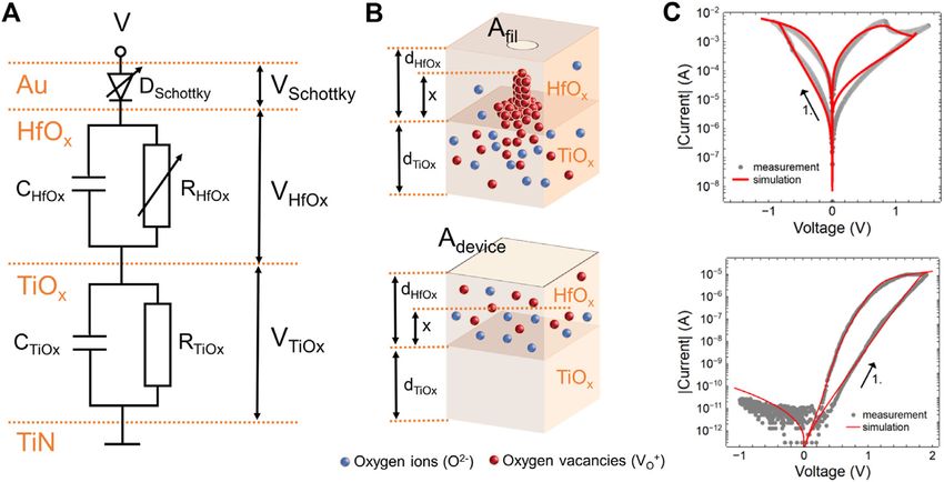
Park et al.                                                                                                 Tailoring Bi-Layer Oxide Memristive Devices

1 INTRODUCTION                                                             et al., 2018; Xiong et al., 2019). The resistive switching mechanism
                                                                           can be described as follows (Cüppers et al., 2019): under an
Memristive devices have been under the spotlight as an ideal               external bias voltage oxygen vacancies are injected from the
element for neuromorphic computing due to their outstanding                reservoir layer into the solid state electrolyte layer in which
characteristics to emulate bio realistic information processing            the oxygen vacancies are forming a filamentary conduction
(Versace and Chandler, 2010; Legenstein, 2015; Mohammad                    path toward the metallic electrode. This reduces both the
et al., 2016; Jeong and Shi, 2019; Krestinskaya et al., 2020).             resistance of the electrolyte layer and the Schottky barrier
Their non-volatile memory property, which is induced by an                 height and leads to a lowering of the overall device resistance
adaptation of the resistance state by applying electrical signals,         (Asanuma et al., 2009; Zhao et al., 2020). An alternative concept
makes them ideal candidates for the emulation of synaptic                  of a memristive bi-layer metal oxide device is the double barrier
functionalities in artificial neural networks (Sah et al., 2014).           memristive devices (DBMD) (Hansen et al., 2015). In this device
For this application, they enable the realization of extremely             structure, an ultra-thin solid electrolyte layer is sandwiched
energy-efficient hardware (Massimiliano and Yuriy, 2013;                    between a metal oxide layer and a metal electrode forming a
Ignatov et al., 2017) and have the potential of a high                     Schottky-like contact. Here, the metal oxide layer serves as a
integration capability due to their simple two-terminal device             diffusion barrier for oxygen ions, but not as a reservoir (Hur et al.,
structure (Lin et al., 2020). In particular, the integration of            2010; Yin et al., 2015; Clima et al., 2016; Dirkmann et al., 2016;
memristive devices in crossbar structures is worthy of                     Hansen et al., 2017). The resistive switching effect is based on a
mentioning here, which makes it possible to implement                      shift of the oxygen ions in the solid state electrolyte layer in the
efficient learning schemes (Prezioso et al., 2015; del Valle                direction of the metal electrode, which also leads to a reduction of
et al., 2018; Alibart et al., 2013).                                       the Schottky barrier height (Dirkmann et al., 2016). The
   When considering the wide range of different neuromorphic               advantage of the non-filamentary type of devices is that they
systems, two main fields of applications in neuromorphic systems            did not require an electroforming step (Yoon et al., 2014), and the
can be distinguished (Ielmini and Ambrogio, 2020): (i)                     switching effect is based on a defined interface effect (Govoreanu
neurobiologically realistic learning schemes and (ii) machine              et al., 2013). However, a disadvantage compared to bi-layer metal
learning based algorithms. In neurobiologically realistic                  oxide devices with oxygen vacancy filaments is the shorter
learning schemes the synaptic connections of a network are                 retention time (Solan et al., 2017). Furthermore, DBMDs have a
tuned by time-encoded spike-like signals (Snider, 2008), which             rectifying characteristic (Gao et al., 2015) and thus a high
typically requires nonlinear memristive device characteristics in a        asymmetry in the voltage polarity. However, these devices allow
time-dependent manner (Ziegler et al., 2015; Dittmann and                  the realization of selector-free crossbar structures (Ma et al., 2017;
Strachan, 2019). In contrast to that, machine learning based               Hansen et al. 2018) and the realization of biologically realistic
algorithms use vector-matrix multiplications in which an                   computational schemes (Wang et al., 2015; Diederich et al., 2018).
explicit time dependence is not required (Ziegler et al., 2018).               A common challenge in the development of memristive
For that application, it is more important to set very precisely           devices is a tailor-made design of memristive devices for a
different resistance values for the individual memristive cells in a       respective computational scheme (Pei et al., 2015). For this, a
crossbar array (Yakopcic et al., 2015). Therefore, a time-                 number of materials and technology parameters have to be
independent linear resistance modulation is desirable                      considered, such as the concentration of oxygen vacancies (He
(Chandrasekaran et al., 2019) which requires a high symmetry               et al., 2017) or active ions (Clima et al., 2016), materials for the
between the setting and the resetting characteristic of the                active layers and interface (connecting) layers (Li et al., 2018b).
memristive device over a wide range of resistance states                   But also geometrical parameters such as layer thicknesses (Park
(Wang et al., 2016).                                                       et al., 2015; Wang et al., 2016; Li et al., 2018a) and size of the active
   In last couple of years many memristive device structures have          areas (Lee et al., 2010) have to be considered carefully. These
been presented that are adequate for the machine learning                  parameters are often only slightly known or not known at all but
algorithms (Kim et al., 2017; Cüppers et al., 2019; Li et al.,             must be related to the device performance for a reliable device
2020; Yao et al., 2020). It has been shown that the use of the             functionality (Niu et al., 2010; Lee et al., 2011). This particularly
memristive devices can significantly simplify the training routine          requires systematic investigations of the individual parameters
in massively interconnected networks (Wang et al., 2019).                  and suitable device technology combined with a profound
Among those devices, particularly, memristive devices with a               understanding of the underlying physical processes (Sun et al.,
metal oxide bi-layer structure gained considerable interest in that        2019).
field. Those memristive devices showed a significant                             The aim of this work is to bridge the gap between the material
improvement in the resistance modulation linearity (Li et al.,             design and the electronic characteristics of memristive devices for
2018a) and the number of resistance states (Stathopoulos et al.,           a tailored development of bi-layer metal oxide devices for
2017) along with the reduced variability in the resistive switching        neuromorphic systems. For this purpose, the bi-layer system
characteristics (Wang et al., 2010). The bi-layer metal oxide              TiN/TiOx/HfOx/Au is examined in more detail in this paper.
devices typically consist of an oxide layer that serves as a               In detail, a four-inch wafer technology is presented, which allows
reservoir of oxygen vacancies and a solid state electrolyte layer          to vary different device parameters, such as layer thickness and
which builds a Schottky-like interface contact with the adjacent           area size of the devices over the wafer. Using automated electronic
metallic electrode (Huang et al., 2012; Bousoulas et al., 2016; Kim        measurements, a statistic of important device characteristics is

Frontiers in Nanotechnology | www.frontiersin.org                      2                                         April 2021 | Volume 3 | Article 670762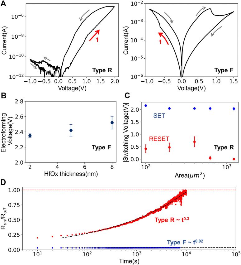
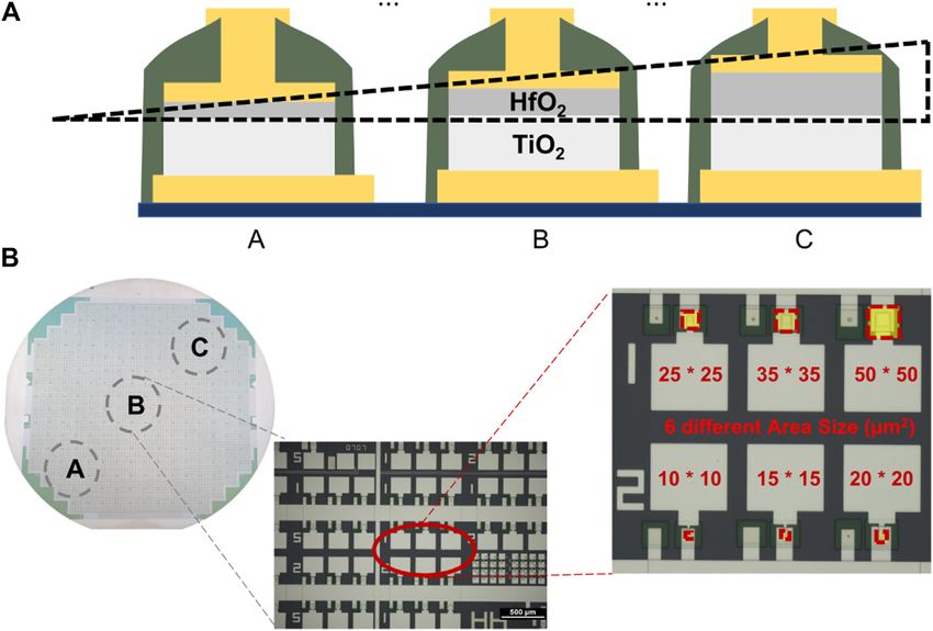
Park et al.                                                                                                                           Tailoring Bi-Layer Oxide Memristive Devices

  FIGURE 1 | Schematic representation of the technology for bi-layer oxide memristive devices: Using different sputtering geometries (referred to as methods 1 and 2
  in the text), different types of devices have been produced, showing filamentary switching (referred to as type F) and area-based resistance switching (referred to as type
  R). (A) Cross-section of TiN/TiOx/HfOx/Au bi-layer oxide memristive devices over the wafer. The used deposition method (method 2) allows for a variation of the thickness
  of HfOx layer from 2 to 8 nm. (B) Microscope images of a complete 4-inch wafer with 40,000 single devices and sections, showing the individual cells which consist
  of clusters with six devices, each with a different area size. Three regions on the wafer are indicated as A, B, and C. Each region has an area size of 0.5 × 0.5 cm2. For type
  R devices a 2 nm HfOx was deposited on all the three regions, while the thicknesses for type F have 2, 5, and 8 nm HfOx films on region A, B, and C, respectively. Here, it
  was assumed that the HfOx thickness is the same in each region due to the 1-dimensional thickness change over a 4-inch wafer and the relatively small area size.
  Approximately 60 memristive devices were measured in each area A, B, and C, respectively, for type F.

collected, and related to material properties and technology                                 presented and discussed. For this purpose, first, the results of the
parameters. For a detailed understanding of the resistive                                    electrical measurements and their statistics are shown in relation
switching mechanism, a physical device model is presented,                                   to an individual device and technology parameters. Then,
which also allows a detailed examination of the individual                                   important parameters of the devices are related to their
device parameters. Essentially, we show that different                                       electronic characteristics using the simulation model. Finally,
sputtering conditions can influence oxygen ion and oxygen                                     the chapter discusses the application of the devices in
vacancy concentrations in the HfOx layer. This causes                                        neuromorphic computing architectures. The presented results
different device characteristics. While an area-based switching                              are summarized in chapter 4.
mechanism leads to a rectifying current-voltage characteristic at
high layer qualities with few oxygen vacancies, filamentary
structures are formed in the HfOx layer at higher                                            2 MATERIALS AND METHODS
concentrations of oxygen vacancies. This leads to a
symmetrical current-voltage characteristic with multilevel                                   2.1 Device Technology
resistant states and improved retention. In both cases, a                                    Figure 1 shows a developed device technology for bi-layer oxide
change in the Schottky barrier between the HfOx layer and the                                memristive devices. In Figure 1A cross-sections of the fabricated
Au electrode can be identified as the reason for the observed                                 TiN(50 nm)/TiOx (30 nm)/HfOx (2–8 nm)/Au(50 nm) bi-layer
switching effect. For a tailored design of memristive devices for                            memristive devices with Al(300 nm) contact pads are sketched.
their application, the different electronic characteristics are                              They are fabricated on a 4-inch oxidized silicon wafer (1 μm of
related to possible applications in neuromorphic systems.                                    thermal SiOx) in the full device technology. This technology is
   The present work is structured as follows: In chapter 2, the                              overviewed in Figure 1B and contains around 40,000 single
implemented technology for manufacturing the memristive                                      devices, including test structures for the device development
devices is presented first. Then the used methods for material                                (see microscope images in Figure 1B). This allows the
and electrical characterization of the devices are discussed.                                investigation of various device parameters, such as the active
Finally, chapter 2 presents a physical device model that serves                              device area (six different area sizes are realized, as shown in
to describe the underlying physical effects of the resistive                                 Figure 1B), the thickness of the active HfOx layer, and the
switching mechanisms. In chapter 3, the obtained results are                                 material compositions over the wafer for a targeted

Frontiers in Nanotechnology | www.frontiersin.org                                        3                                                 April 2021 | Volume 3 | Article 670762
Park et al.                                                                                               Tailoring Bi-Layer Oxide Memristive Devices

development of memristive devices. For a variation of the latter          2) deposited HfOx films. Thus, in agreement with previous
parameter, two different sputtering methods for the HfOx layer            investigations (Martínez et al., 2007) the film can be assumed
were used. In particular, a variation in oxygen vacancies is              to have amorphous crystallinities. However, the obtained n value
required to achieve a desired resistive switching process in this         from the uniform deposited film was higher than n of the wedge
class of memristive devices (He et al., 2017). Here, using a              deposited HfO2 film, which can be attributed to a reduced
sputtering system equipped with three confocal source targets,            packing density (Gao et al., 2016).
two methods are employed for the deposition of the HfOx which                Furthermore, X-ray photoelectron spectroscopy (XPS)
are referred to as method 1 and 2. During the deposition, the             measurement was utilized to study the quantitative atomic ratio
substrate is rotated to obtain a uniform film thickness, while a           O/Hf in sputtered HfOx layers. The XPS analysis were carried out
wedge film is formed without a rotation. The wedge is formed               using monochromatic Al_K-alpha radiation (excitation energy
only along one direction. For method 1 the HfOx layer was                 hν  1,486.68 eV) under charge neutralization using a SPECS
deposited on the wafer under optimal conditions, i.e., rotation of        SAGE HR 150 XPS system equipped with a 1D delayline detector
the substrate within a confocal sputtering arrangement. For               and a Phoibos 150 analyzer. The calibration of the energy scale was
method 2 the wafer was not rotated during the sputtering of               ensured by reference measurements on a polycrystalline silver
the HfOx layer. This leads to a reduced layer quality, but also a         sample. Before the measurements, HfOx was sputtered on Si/
wedge over the wafer as shown in Figure 1A (further details are           SiO2 wafers for 900 s using the two different sputtering method
discussed below). As a result, we obtained two distinctive bi-layer       1 and 2. As a result, a ratio of O/Hf of 1.80/1 was observed for
oxide memristive device structures, which are referred to in the          deposition method 2, while a ratio of 1.98/1 was recorded for
following as device R and device F.                                       samples sputtered via method 1 (see Supplementary Data S1). The
    In more detail, the TiOx/HfOx bi-layer was deposited on an            sputtering method 1 provides a stoichiometry close to HfO2, while
inertial reactive sputtered TiN bottom-electrode via DC                   the obtained stoichiometry via method 2 leads to optimal condition
magnetron sputtering, where O2/Ar of reactive gas was                     for the forming of oxygen vacancy filaments (McKenna, 2014).
adjusted with the ratio of 10/40 and 10/29 for the TiOx and               Thus, we can conclude that sputtering method 1 leads to a reduced
HfOx film, respectively. After the TiOx was sputtered, the                 number of oxygen vacancies than the sputtering method 2. Hence,
thickness of the HfOx was controlled using the two discussed              a HfOx layer with a higher density of oxygen vacancies can be
sputtering methods 1 (for device type R) and 2 (for device type F):       assumed for device type F in respect to device type R.
as seen in Figure 1A a wedge layer with a variation of the HfOx
thickness from 2 to 8 nm was obtained for device F, where devices         2.3 Electrical Characterization
were fabricated along the axis (x-direction) perpendicular to the         Current-voltage measurements (I-V curves) and voltage pulse
axis of the wedge (y-direction). Device R has a 2 nm uniform              measurements were carried out to characterize the electrical
HfOx layer. The layer deposition was finalized with an Au top-             properties of TiOx/HfOx bi-layer memrsitive devices using a
electrode layer. Thereafter, the material stack was patterned using       source measurement unit (Keysight b2901a). Therefore, a
photolithography and reactive ion etching for device R, while a           voltage is applied to the top-electrode of the device (bottom-
lift-off in Dimethylsulfoxide (DMSO) was used for device F. The           electrode were grounded), while the current has been measured
lift-off process was carried out due to the thickness variation of        simultaneously. Furthermore, current compliance was imposed
HfOx in device F. Here, the investigation of the switching                during the measurement to prevent the device from damage. The
behaviors was preceded after we confirmed that the two                     used current compliance was ICC  10 μA, ICC  −5 mA for R and
patterning methods scarcely affected electrical characteristics.          F devices, respectively. For pulse measurements the device
All devices were insulated with SiO2 layers from the ambient              resistance was measured at, respectively, 1 and 0.1 V for R and
air to avoid the influence of moisture in switching behaviors              F devices. The switching voltage to set and reset the device
(Tsuruoka et al., 2012; Zhou et al., 2018; Zhou et al., 2020)             resistances was 3 V/−2 V for device type R and −1 V/1.5 V for
(Figure 1A), and Al contact pads were deposited by e-beam                 F type devices. For both devices a pulse duration of ∼10 ms was
evaporation.                                                              used. For a statistical evaluation of the electrical properties, median
                                                                          values were extracted taking into account the variability in cycle to
2.2 Material Characterization                                             cycle (C2C), and device to device (D2D). In the C2C investigation
The development of the memristive devices was supported by a              10 times of DC voltage sweep cycles in one device were carried out.
material characterization accompanying the manufacturing                  For reliable statistics, automated measurements of more than 10
process. The thickness and the composition of the layers were             memristive devices in each device parameter were performed,
characterized by ellipsometry measurements (SE500, Sentech)               which means a total of 180 devices measured for three different
and surface profile measurements (Dektak 150, Veeco).                      thicknesses and six different area sizes. Both C2C and D2D
   For a detailed material investigation, unstructured HfOx films          statistics were investigated in DC conditions.
were deposited on silicon substrates. Therefore, the two described
sputtering methods 1 and 2 were employed to deposit 37 nm                 2.4 Physics Based Device Model
thick HfOx films. On those films ellipsometry measurements were             For a profound understanding of the resistive switching
performed at 632.8 nm at 70° of incidence. As the results,                mechanisms and a targeted development of the devices a
refractive indices of n  1.9889 and n  2.0285 were measured             physics based device model was developed. In Figure 2A a
for, respectively, the uniform (method 1) and the wedge- (method          sketch of this device model is shown: the model consists of

Frontiers in Nanotechnology | www.frontiersin.org                     4                                        April 2021 | Volume 3 | Article 670762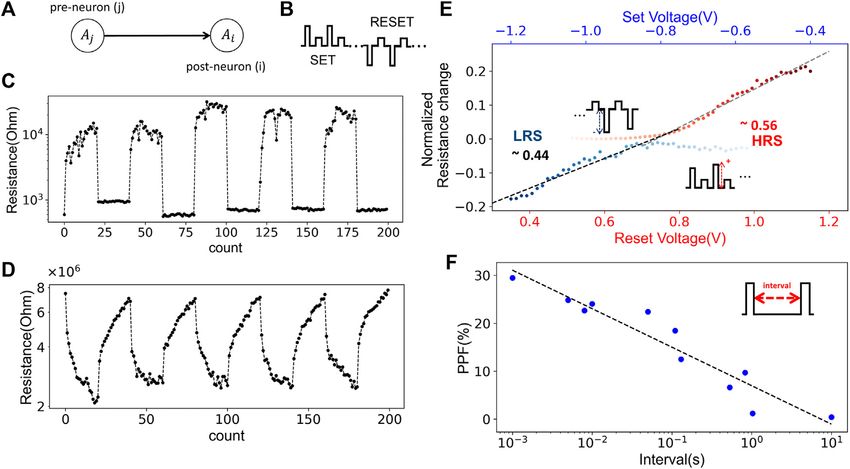
Park et al.                                                                                                                       Tailoring Bi-Layer Oxide Memristive Devices

  FIGURE 2 | (A) Sketch of the physics based device model for TiN/TiOx/HfOx/Au memristive devices. The model consists of two RC elements in the TiOx and HfOx
  layers and a Schottky diode at the interface of HfOx and Au top-electrode. The external source voltage is divided into three local voltage drops at the HfOx, TiOx layers,
  and the Schottky diode. (B) Two different resistive switching mechanisms of type F devices (top) and type R devices (bottom) are considered. While in type F devices
  oxygen vacancies form a filamentary conductive path in the HfOx film under an external voltage, in type R devices oxygen ions in the HfOx film drift toward the top
  metal-electrode. As a result, in both device types the changed ion concentration leads to a modulation of the Schottky barrier height, which leads to the switching
  behaviors. Hereby originates the difference in the switching mechanisms from the density of the oxygen vacancies in the HfOx film. (C) Measured I-V curves (gray) and the
  simulation results (red) for type F (top) and type R (bottom) devices. The arrows point to the SET direction.

two RC elements representing, respectively, the HfOx and the                               device the whole device area is involved in the switching
TiOx layer. The metal-semiconductor contact between the HfOx                               mechanism, i.e., A  Adevice (see lower drawing in Figure 2B).
layer and the Au electrode is considered by a Schottky diode                               Both, the active area and the oxygen ion/vacancy
(DSchottky ). Thus, an external applied voltage (V) is divided into                        concentration, are relevant for the resistance of the HfO x
the local voltage drops at the Schottky diode (VSchottky ), over the                       layer:
HfOx layer (VHfOx ) and the TiOx layer (VTiOx ) according to
                                                                                                                                      dHfOx
                                                                                                                     RHfOx                                                    (2)
                        V  VSchottky + VHfOx + VTiOx                            (1)                                           e · zv0 · A · μn · N
An important difference between here investigated two types of                             where μn is the electron mobility, zv0 is the ion charge number,
memristive devices is sketched in Figure 2B. While for the type F                          and e is the elementary charge (Hardtdegen et al., 2018).
device a filament of oxygen vacancies is formed under the                                       The layer thickness of TiOx is significantly larger than that of
external voltage application, the type R device does not form                              HfOx. Therefore, a much lower local electrical field strength is
any filaments. Essential for this is the concentration of oxygen                            assumed (E  Vlayer /dlayer ). Thus, under an external bias voltage
ions and vacancies in the active HfOx layer (Dirkmann et al.,                              oxygen ion drift is suppressed within the TiOx layer and the
2018). For the filamentary device F, we assumed that a number of                            resistance RTiOx of the TiOx layer can be assumed to be constant.
oxygen vacancies are the mobile ions that vary between a                                   Nevertheless, the TiOx layer plays a crucial role in the
minimum and a maximum concentration, denoted as Nmin                                       functionality of the bi-layer oxide structure: (i) it serves as a
and Nmax , respectively. In detail, for the filamentary device F                            reservoir for oxygen vacancies in filament devices, and (ii) it
we estimated Nmin  4 · 1024 m−3 and Nmax  2 · 1027 m−3 in                                stabilizes the switching process for both types of devices
accordance with the previous work (Menzel et al., 2011;                                    (Stathopoulos et al., 2017; Hardtdegen et al., 2018; Mikhaylov
Dirkmann et al., 2018). On the other hand, for the device type                             et al., 2020). For the latter point, the electronic contribution of the
R we assumed a significantly lower concentration of oxygen                                  TiOx layer is particularly important and has to be captured in the
vacancies due to a better layer quality. Here, the mobile                                  model. In general, the electronic charge transport through metal
species are oxygen ions where a concentration of N  1023 m−3                              oxide layers can be determined by various transport mechanisms.
was used which is in qualitative agreement with (Dirkmann et al.,                          It has been shown that a good approximation for the electron
2016).                                                                                     current is given by the following voltage realization (Jiang et al.,
    The concentration of the oxygen ions and vacancies has a                               2016):
particular effect on the active area used for resistance
switching (cf. Figure 2B). Thus, for the filamentary device                                                           ITiOx  j0 · A · sinh(VTiOx )                             (3)
F only the filament area is relevant for the switching effect,                              where j0 is a fit parameter that has to be adapted to the real
i.e., A  Afil (see upper drawing in Figure 2B). For the type R                            devices. The layer capacitances are given by

Frontiers in Nanotechnology | www.frontiersin.org                                      5                                               April 2021 | Volume 3 | Article 670762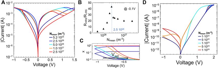
Park et al.                                                                                                         Tailoring Bi-Layer Oxide Memristive Devices

                                               A                                 thermionic emission theory, the charge transport over a Schottky
                                Clayer  ε                             (4)
                                             dlayer                              barrier can be described in the following equation (Sze and Ng,
                                                                                 2006):
where ε  εr ε0 is the permittivity of the respective layer.
                                                                                                                         eV
   The starting point of the switching model is the memristive                                          IS  IR expnVT − 1                              (10)
behavior caused by a temporal and spatial change of the oxygen
ions in the HfOx layer. This effect is taken into account in the                 Where n is the ideality factor, which describes the deviation from
device model via an average ion velocity.                                        an ideal diode characteristic, and IR the reverse current, which is
                                dx                                               given by:
                                    cdrift · IIon                     (5)                                                       − eϕB
                                dt
                                                                                                        IR  A* AT 2 · exp VT                            (11)
where x is the memristive state variable, i.e., the average position
of oxygen ions or length of the filament in the HfOx layer (cf.                   where A* is the effective Richardson constant, which is
Figure 2B) and IIon is the ionic current of the oxygen ions.                     1.20173 · 106 Am−2 K −2 , T the local temperature, and A the
Furthermore, cdrift describes the resulting drift constant of the                active area. Under negative voltage polarities, however, the
system, which is defined as                                                       reverse current decreases gradually with the applied bias
                                                                                 voltage. Therefore, on this polarity the reverse current is (Sze
                                          μn · Rmean                             and Ng, 2006):
                               cdrift                                 (6)
                                          dHfOx · A                                                                           − eϕB
                                                                                                                                             √
                                                                                                                                         − eαr |V|
                                                                                                IR,v < 0  −A* AT 2 · exp VT exp             VT
                                                                                                                                                         (12)
Here, Rmean is the mean resistance of the HfOx layer, which is
given by Rmean  12 · [Rmin + Rmax ] for devices of type F and                   Here αr is a device dependent parameter. In our model we
Rmean  RHfOx for the devices of type R. In particular, for                      assumed that both quantities n and ϕB depend on the
devices of type F the resistance of the HfOx layer can be                        concentration of moved ions at the Au/HfOx interface. A
specified as a function of the memristive state variable x:                       higher concentration of the negatively charged oxygen ions at
                                                                                 that interface in R type devices increases the electron
                         dHfOx         1       1
          RHfOx                    ·    ·x+      · (1 − x)          (7)       concentration locally. For devices of type F an increased
                    e · zv0 · A · μn Nmax     Nmin                               concentration of oxygen vacancies increases the amount of
An essential important property of ionic based memristive                        acceptor states for electrons at the interface and thus there is
devices is the back diffusion of the ions. The back diffusion                    also an accumulation of electrons at the interface. Thus, for both
determines the reliability and the storage time of the memristive                type of devices a reduction of the Schottky barrier is expected,
device and is crucial parameter for a precise adjustment of                      which in turn has a significant effect on the charge transport
multiple resistance states. In order to consider this behavior in                through the complete device. In the model this was considered by
the model, a further term was added to Eq. 6:                                    a state variable dependency of those quantities:

                          μn · Rmean                                                                             x                            x
               cdrift               − cback · 1 − (2x − 1)2         (8)                    ϕB (x)  ϕLRS
                                                                                                        B ·           + ϕHRS
                                                                                                                         B   · 1 −                     (13)
                          dHfOx · A                                                                            xmax                         xmin
                                                                                                                x                             x
Here cback is a parameter that describes the strength of the back                              n(x)  nLRS ·          + nHRS · 1 −                     (14)
                                                                                                               xmax                        xmin
diffusion and must be adapted to the measured data.
   The ion current can be written in the following form using the                the values for nLRS and nHRS , as well as ϕHRS and ϕLRS
                                                                                                                            B        B were obtained
law of Mott and Gurney (Hardtdegen et al., 2018):                                from the experimental I-V curves using Eq. 10. Another important
                                             ΔW          a · EHfOx               parameter influencing the ion movement within the memristive
         IIon  4AeNmean a]0 · exp−             · sinh             (9)       device is the local temperature change. This includes mainly Joule
                                             VT             VT
                                                                                 heating and plays a crucial role particularly in filamentary-based
where ΔW is the diffusion barrier, which is reduced by the electric              device structures. This was taken into account in the simulation
field EHfOx . Furthermore, VT is the thermal voltage, a the hopping               model as follows (Ielmini and Milo, 2017).
distance, and ]0 is the attempt frequency. Nmean determines the                                        T  I · V · Rtherm + T0                           (15)
mean concentration of mobile ion species in the HfOx layer,
i.e., Nmean  12 · (Nmax + Nmin ), while A is the active area of the             Here, Rtherm is the effective thermal resistance and T0 is the room
device, which depends on the device type (cf. Figure 2B). Thus                   temperature. The temperature along the filament is assumed to be
A  Afil for the filamentary device and A  Adevice for the interface             relatively homogeneous and thus a uniform filament temperature
based switching device (cf. Figure 2B).                                          can be assumed (Ielmini and Milo, 2017).
    The interface between the HfOx/Au is assumed to be the                          The device parameters have been carefully collected from
relevant interface for the resistive switching process in both types             measurements and literature and are summarized in Table 1.
of devices. In the simulation, this interface is modeled as a                    The I-V curves simulated with the model are shown in Figure 2C
Schottky diode with variable Schottky barrier (ϕB ). Using the                   and compared with the measurement curves determined

Frontiers in Nanotechnology | www.frontiersin.org                            6                                           April 2021 | Volume 3 | Article 670762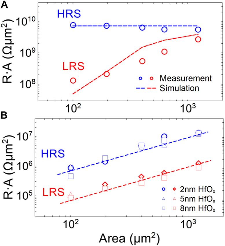
Park et al.                                                                                                                        Tailoring Bi-Layer Oxide Memristive Devices

TABLE 1 | Simulation Parameter.                                                             3 RESULTS AND DISCUSSION
Parameter                       Value                   Parameter            Value
                                                                                            3.1 Resistive Switching and Statistical
                    type F              type R
                                                                                            Examinations
ΦHRS
   B [eV]            0.25                0.71            αr [V/A · s]       1.2 · 106       In Figure 3A typical obtained I-V curves of the two kinds of
ΦLRS
   B [eV]            0.06                0.61           μn [m2 /V · s]        10− 5         memristive devices (named as F and R) are shown. Common for
nLRS                   4.5                3.9               ]0 [Hz]         3 · 1011
nLRS                    5                4.45                εTiOx             17
                                                                                            both device types is that they show bipolar resistive switching
                                                               r
Nmax [m−3 ]         2 · 1027                                 εHfOx
                                                               r               5.5          with a gradual resistance change. A major difference between
Nmin [m−3 ]         4 · 1024                              ΔW[eV]             0.425          both types of devices is their voltage polarity. While type R
N[m−3 ]                                 1023                a[nm]              0.4          devices require a positive voltage (applied to the top electrode)
dHfOx [nm]            2–8                2.5             dTiOx [nm]            30           to set the device, type F devices require a negative voltage to be
 0
jTiOx [A/m2 ]       5.8 · 107         5.8 · 104         Rtherm [K/W]        1.1 · 104
Adevice [μm2 ]                          100               Afil [nm2 ]        6,362
                                                                                            applied for the set process. The different polarity behaviors are
Cback /Cdrift          0            3.25 · 10− 11           T0 [K]            273           originated from differences in concentration and species of
                                                                                            mobile ions, which will be discussed in Concentration of
                                                                                            Mobile Icon. Furthermore, while a highly rectifying memristive
experimentally. As can be seen from this figure, the model                                   behavior is observed for device type R, a more symmetric
presented here shows very good agreement with the                                           memristive behavior is found for devices of type F together
experiment. A more detailed description of the results follows                              with a 3 times higher current level as compared to type R
in the next chapter.                                                                        devices (cf. Figure 3A). In some more detail: the rectifying

  FIGURE 3 | (A) Representative I-V curves of TiN/TiOx/HfOx/Au bi-layer memristive devices for type R (left), and type F (right). The arrows point to the resistive
  switching direction. A clear rectifying behavior was observed in the type R, and a symmetric switching behavior in the type F. (B) Electroforming voltage (median values)
  as a function of HfOx thickness. Electroforming voltages were tailored by the thickness of the HfOx in type F. (C) SET (blue) and RESET (red) voltages (median values) as a
  function of device active area size. The smaller the area is, the lower SET/RESET voltage was observed. (D) Retention measurement and fitting curves. Type F
  devices (blue) showed an improved retention characteristic compared to type R (red). The fitted curves are shown with dashed lines, and the fitting constants were 0.02
  and 0.3 for type F and type R, respectively.

Frontiers in Nanotechnology | www.frontiersin.org                                       7                                               April 2021 | Volume 3 | Article 670762
Park et al. Tailoring Bi-Layer Oxide Memristive Devices
behavior of devices of type R can be quantified by the ratio different activation energies of the ion dynamics. It has been
between the maximum and minimum current rasym Imax /Imin shown that the activation energy of oxygen vacancies is in the
at a voltage of ±0.5 V. Here we were able to determine rasym 70 range of 6–8 eV inside filaments (McKenna, 2014), while it is less
for an active device area of 100 μm2 which, however, has a strong than 1 eV outside filaments (Dirkmann et al., 2016; Dirkmann
area dependence. In particular, for an area of 625 μm2 the et al., 2018). Furthermore, it is worth mentioning that localized
asymmetry ratio rasym is reduced from 70 to 4 (further electronic states at the Au/HfOx interface can also contribute to
information is provided in Supplementary Figure 3). the observed switching mechanism. The localized electronic
An important property of memristive devices and another states are filled or emptied depending on the applied bias
difference between the here considered devices is the initial voltage polarity (Hansen et al., 2015; Zhou et al., 2016). Even
electroforming process. While no initial electroforming step if the exact mechanism underlying the switching effect cannot be
was necessary for type R devices, type F devices had to be clearly explained by the presented measurements alone, the
electroformed at the beginning. For a more precise discussion strong difference in the retention times and the different
of the electroforming process of type F devices, the median of the voltage polarity indicate that oxygen vacancies dominate the
required voltages as a function of the thickness of the HfOx layer respective switching behavior in type F devices, while mobile
is depicted in Figure 3B. In detail, electroforming voltages of 2.35, oxygen ions lead to resistive switching in type R devices.
2.42, and 2.52 V have been observed for, respectively, a 2, 5, and In order to be able to make suitable statements about possible
8 nm thick HfOx layer. Thus, the electroforming voltage shows applications of the memristive devices in neuromorphic systems
moderate thickness scalability. After the electroforming process and to tailor the device characteristics accordingly, a statistical
type F device are operated typically at a maximum (minimum) investigation of relevant device parameters is required. As
voltage ±0.75 V. In terms of operating voltage, type F devices also relevant device parameters we considered the thickness of the
differed from type R devices: type R devices require on average a active HfOx layer (dHfOx ), the active area size A, and the
1.3 V higher operating voltage with a moderate area dependence concentration of mobile ions N. The results of that
(cf. Figure 3C). The operating voltages for type R devices were investigation are shown in Figure 4. In the cumulative
2.2 V/−0.42 V (SET/RESET) for the smallest area size and 1.7V/ distribution function (CDF) of the resistance of type R devices
0 V for the largest area size. However, the type R devices show a (Figure 4A) and of type F devices (Figure 4B) the resistances
more gradual transition from the inertial high resistive state were obtained from voltage sweep measurements by calculating
(HRS) to the low resistive state (LRS) (cf. Figure 3A). the corresponding median values and the standard deviations.
A crucial property of memristive devices is their retention The resistance obeyed a lognormal distribution for all examined
time. Furthermore, a detailed investigation of the retention devices. For devices of type R (cf. Figure 4A) the resistance
characteristic already provides important conclusions about distributions for area sizes from 100 to 1,225 µm2 are shown. For
the underlying resistive switching mechanism (Hansen et al., the devices of type F the different curves in Figure 4B originate
2015). The retention behavior for the here discussed two types of from the different dHfOx . As a result, we found that for devices of
memristive bi-layer structures are shown in Figure 3D. For the type R the resistance window decreased with increasing active
measurement of the retention characteristics, the two types of area size A which can be attributed to the decreasing rectifying
devices were initially set to the low resistance state and then the ratio (further details are in the supplement). Furthermore, the
resistance value of the devices was determined at regular intervals relatively small width of the CDF curve was observed for type R
by means of voltage pulses. As can be seen in the figure, the two devices indicating a high device uniformity. For the devices of
types of devices show quite different retention behaviors. For type F, the low resistant states show a steeper change in the CDF
device type R, diffusive characteristics were observed (see red data curve than the high resistant states. Even though the found
points in Figure 3D), while much higher retention is observed for variations in the resistances are small, the devices with a HfOx
device type F. In order to analyze the retention characteristics in thickness of 5 nm show here the best variability.
some more detail the retention curves were fitted using a power To be able to make detailed statements about the requirements
law according to the Curie-von Schweidler equation (Mikheev to be met by the physical device parameters, the influence of the
et al., 2014; Goossens et al., 2018): variability in relation to the physical parameters must be
examined. Therefore, normalized standard deviations of the
R Ron Roff ∝ t α (16) devices were determined and plotted as a function of the
active volume, i.e., the layer thickness of the active HfOx layer
where α is a fit parameter, which is between 0 and 1 (Yang et al., times the device area. The obtained results for both types of
2010). As a result, α 0.3 is observed for devices of type R, devices are shown in Figure 4C. The figure shows the different
whereas α 0.02 best reflects the experimental data for devices of measured variabilities for the devices of type R (triangular data
type F. While α 0.02 describes a very good retention time for points) and the devices of type F (circular data points) as a
devices of type F, α 0.3 shows clearly lower retention for devices function of the active volume of the device. For devices of type R it
of type R. This difference can be explained by the different ion appears that the variability is only weakly affected by increased
dynamics between the two devices. While in the type R device the area size. Here the normalized standard deviation of 0.2 is quite
filamentary structures are suppressed and mobile oxygen ions are constant over the investigated area sizes (see the dashed black line
shifted toward the electrode, in the type F devices oxygen in Figure 4C). However, for devices of type F a parabolic curve
vacancies are organized in filamentary structures. This leads to best describes the found trend which indicates a clear optimum at
Frontiers in Nanotechnology | www.frontiersin.org 8 April 2021 | Volume 3 | Article 670762Park et al. Tailoring Bi-Layer Oxide Memristive Devices
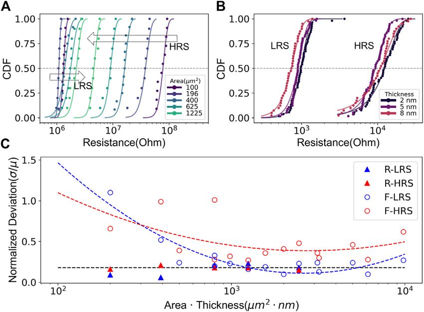
FIGURE 4 | Resistance distribution for different physical device parameters in type R devices (A), and type F devices (B). (A) CDF for different active device area
sizes of device type R. The arrows point to the direction of the increasing area. (B) CDF for different HfOx thicknesses in type F devices. (C) Device variability (σ/μ) in terms
of physical device parameters. The variability of type R devices is marked with triangles, and type F devices with circles. Red color for high resistance states, and blue
color for the low resistance were used. The fitted curves are shown with dashed lines. For type F devices a parabolic trend was observed, which shows a correlation
between the area and the thickness of the HfOx in the variability of devices.
approximately 2.6 · 103 μm2 · nm for the HRS and 2.73 · 103 μm2 · the mentioned points (i–iii) will be discussed in the following in
nm for the LRS. This means that a reduction from dHfOx 8 nm to more detail.
dHfOx 2 nm increases the optimal device area from Adevice
(18 × 18) μm2 to Adevice (36 × 36) μm2 . Thus, the trend can be 3.2.1 Schottky Barrier Height Lowering
observed that with extremely small layer thicknesses, a larger area From the measured I-V curves the minimum and the maximum
leads to a more stable device behavior. values of the variation of the Schottky barrier were determined.
Therefore, Eq. 11 was adapted to the experimental data at the
voltage interval ranging from 0 to 100 mV for both device types.
3.2 Resistive Switching Mechanism and Furthermore, we made the assumption that the resistance of the
Device Requirements device does not change in that interval. As a result, we found that
A sound understanding of the resistive switching mechanism is the values for the Schottky barriers vary between 65 meV and
important to enable a targeted design of the memristive devices 250 meV for the filamentary device F (upper graph in Figure 2C),
for application in neuromorphic systems. For this reason, the whereby a barrier variation of 615 meV and 708 meV was
device model described in Physics Based Device Model was used obtained for the area-based device R (lower graph in
to interpret the experimental results described above. The Figure 2C). In addition, the fit procedure also considered the
obtained results are shown in Figure 2C. Therein the ideality factor as an adjustable parameter, whereby we obtained
experimental I-V curves are compared with simulated curves. 5.0 and 4.54 for filamentary device F and 3.9 and 4.45 for the area-
The used simulation parameters are summarized in Table 1. In based device R. A key finding from that analysis is that area-based
both cases, i.e., in the case of the filamentary (type F device) and device has a much higher Schottky barrier, while for both devices
the interface-based device (type R device), one can see quite a strong variation of the Schottky barrier is observed. In order to
good agreement between simulation model and experiment. analyze that finding in more detail, simulations were carried out
The main difference between the two I-V curves in the with a maximal barrier lowering of 200 meV. The results of the
simulation model comes from (i) differences in concentration simulations for the two device types are shown in Figure 5. The
and species of mobile ions due to stoichiometric differences obtained changes in the resistance value for the type R
between Hf and O, (ii) different active areas that are responsible (Figure 5A) and type F devices (Figure 5B) are shown. For
for the switching behavior (cf. Figure 2C), and (iii) the lowering this purpose, the Schottky barrier of the high ohmic state (see
of the Schottky barrier and the change of the ideality factor. In indicated ϕHRS
B in the figures) was used as a starting value and the
order to understand more exactly the underlying switching barrier height was successively reduced, i.e., ΔϕB (ϕHRS
B − ϕLRS
B ).
mechanisms that lead to the different device characteristics, This confirms the experimentally observed finding of a strong
Frontiers in Nanotechnology | www.frontiersin.org 9 April 2021 | Volume 3 | Article 670762Park et al. Tailoring Bi-Layer Oxide Memristive Devices
FIGURE 5 | Influence of the Schottky barrier height lowering ΔΦB on the device resistance: the resistance value as a function of Schottky barrier lowering for type R
devices (A) and type F devices (B). ΦHRS
B is the inertial Schottky barrier height for the respective R and F type device. (C) Asymmetry as a function of the barrier lowering.
Strong asymmetric characteristics are observed in device R (circle) within 200 meV in the barrier lowering, while the asymmetry was destroyed in device F (triangles) at
100 meV barrier lowering.
dependence of the resistance change of the devices on the asymmetry, whereas 100 mV of the type F devices is sufficient to
maximum barrier lowering for both types of devices. Two completely destroy the asymmetry.
types showed different switching mechanisms: filamentary-
and interface-type. However, Schottky contact adjustment was 3.2.2 Concentration of Mobile Ions
an essential factor in resistive switching behaviors for both typem One of the most important parameters for the resistance
F and type R devices. Thus, it can be stated that the Schottky switching mechanism of memristive devices is the
barrier change is the main reason for the switching behavior of concentration of mobile ions. In the simulation model we
the two different memristive devices, which is in good agreement have, therefore, investigated the concentration of mobile ions
with previously published data (Hansen et al., 2015; Hardtdegen in the HfOx layer as a further central device parameter. It turned
et al., 2018). out that for the rectifying device R a constant low concentration
In fact, a significant influence on the Schottky barrier height of negatively charged oxygen ions (Nmin Nmax 1023 m−3 ) best
and therewith an important technology parameter is the material describes the experimental I-V curve, where a variation of
used for the electrode and the oxide layer. Since the same positively charged oxygen vacancies from Nmin 4 · 1024 m−3
electrode material (Au) was used for both types of devices, the to Nmax 2 · 1027 m−3 for the filamentary device F gives the
observed difference can only come from the HfOx layer. In this best agreement with the experiment (cf. Figure 2C). These
respect, the difference is mainly in the layer quality due to the obtained results are in good agreement with previous
different manufacturing processes that we used for the two investigations (Dirkmann et al., 2016; Hardtdegen et al., 2018)
devices. This has a particular effect on the number of oxygen and support the model outlined in Figure 2A. In order to
ions and vacancies, which we will discuss in more detail below. investigate these variations, the concentration of oxygen
However, a qualitative indicator of contact quality is the vacancies was varied in the range from 5.2 · 1025 m−3 to 2.5 ·
asymmetry between the minimum and the maximum current 1027 m−3 for F type device and a variation from 1 · 1022 m−3 to
values in the I-V characteristics and the ideality factor n of the 1 · 1024 m−3 of oxygen ions were used for the rectifying device
contacts. Here we observe that n is lower for the type R devices type R. The simulation results are summarized in Figure 6.
than for the type F devices and the type R devices show a clear Figure 6A shows I-V curves for the filamentary device with
asymmetry and therefore a stronger rectifying characteristic. To different mean concentrations of oxygen vacancies. In particular,
investigate this point, the asymmetry as a function of the barrier two major trends for the change in oxygen vacancies can be seen:
lowering ΔϕB is shown in Figure 5C. The asymmetry was (i) the hysteresis shows a clear variation with the change of the
determined by the following formula: oxygen vacancies, and (ii) the values for set and reset voltages
[(Imax − Imin )/(Imax + Imin )]. As a result, we found that the become smaller. To interpret these two properties in more detail,
barrier lowering of the area-based devices does not affect the Figure 6B shows the ratio RHRS /RLRS at −0.1 V as a function of the
Frontiers in Nanotechnology | www.frontiersin.org 10 April 2021 | Volume 3 | Article 670762Park et al. Tailoring Bi-Layer Oxide Memristive Devices
FIGURE 6 | Simulated I-V curves of TiN/TiOx/HfOx/Au bi-layer memristive devices with a variation of the mean concentration of mobile ions in the HfOx layer. (A) The
variation of the mean concentration of positively charged ions in the range from 5.2 · 1025 m−3 to 2.5 · 1027 m−3 is simulated for type F. (B) The ratio of RHRS /RLRS at −0.1 V
as a function of the mobile ions. The optimum memristive hysteresis was observed at the mobile ion concentrations of 2.5 · 1026 m−3 . (C) The state variable (x) as a
function of the applied voltages for different concentrations of mobile ions in the HfOx layer. Operating voltages (SET/RESET voltage and threshold voltage) in the
bi-layer memristive devices were affected by the concentration of mobile ions in the HfOx layer. (D) The variation of the concentration of negatively charged ions in the
range from 1 · 1022 m−3 to 1 · 1024 m−3 is simulated for type R. The resistance values and the hysteretic effects were influenced by the concentration of oxygen ions.
concentration of oxygen vacancies. What can be seen very clearly
is that there is an optimum of the ratio at 2.5 · 1026 m−3 . The
reason for this is the threshold value of the oxygen diffusion,
which essentially determines RHRS and RLRS . For this purpose,
Figure 6C shows the state variable x as a function of the applied
voltage for the different concentrations at oxygen vacancies.
According to Eq. 7, the concentration of the oxygen vacancies
determines the change of the resistance of the active HfOx layer,
but also the ion drift (see Eq. 6), and thus the change of the state
variable x. What can be observed from the simulation is that high
oxygen vacancy concentrations cause a change in the state
variable already at very low voltage values (cf. Figure 6C).
This means that a threshold value for setting the device can
no longer be set precisely, which already leads to a reduced
resistance value for a voltage of −0.1 V. However, since threshold
values are important for the application, a precise setting of the
oxygen vacancies is an important device parameter that should be
chosen carefully.
The results for the rectifying memristive device under varying
concentrations of oxygen ions are shown in Figure 6D. Here it
can be seen that the concentration of oxygen ions has an effect on
the change of the resistance value as well as on the retention
characteristics. Thus, at extremely low concentrations of oxygen
ions, only small hysteric effects are observed, while a pronounced FIGURE 7 | The R · A product as a function of the device active area for
hysteresis is only observed at a concentration of 5 · 1022 m−3 . This (A) type R and (B) type F. The dashed lines present simulated device models.
concentration of oxygen ions, thus, defines a critical minimum for (A) The R · A product showed a constant behavior in HRS for type R, while an
area dependent behavior for type F (B). The area dependency of the
memristive switching behavior.
R · A product in LRS for device R (A) was caused by the area dependency of
the ion drift constant, which was in good agreement with the simulation
3.2.3 Area Dependence results.
An experimentally important indication of the type of resistive
switching mechanism is given by the area dependence of the
devices. For this purpose, the product of area times resistance and the dashed lines are the results of the simulation model. The
(RA) as a function of the area of the devices is shown for both expected trend can be seen for the high resistant state of the
device types in Figure 7. While the upper graph of Figure 7 is devices: for the filamentary device F, an area independent
presenting the results from the rectifying device R, the graph on behavior is seen, while a clear area dependence was found for
the bottom is showing the area dependency for the filamentary the rectifying device R. It is noticeable that the low ohmic state of
device F. Here, the data points are taken from the measurements the rectifying device R shows a non-uniform area dependence.
Frontiers in Nanotechnology | www.frontiersin.org 11 April 2021 | Volume 3 | Article 670762Park et al. Tailoring Bi-Layer Oxide Memristive Devices
One would actually expect a horizontal line in the R · A vs. A To convert that equation into hardware, the coupling strength ωij
representation chosen here. This is relevant with the drift can be represented by the conductance Gij of the memristive
constant cdrift from Eq. 8, which depends on the layer device, and yj , pj , and dj by voltage- or current-dependent
thickness of the HfOx layer (dHfox ) and the active device area functions that either increase or decrease the conductance of
(A). While the changes in the layer thicknesses (dHfox ) in the the memristive device (Linares-Barranco et al., 2011). Thus, for
experimentally investigated interval cause only a small change in the implementation of memristive devices in neuromorphic
cdrift , the changes in the area for the rectiyfying device R have a network structures via the delta rule a precise change of the
considerable influence on cdrift . In this case, the drift constant conductance in dependence on applied voltage (or current) pulses
(cdrift ) is reduced, especially for large active areas, and thus a is required (Payvand et al., 2018).
smaller change in the state variable x is induced during a voltage In order to investigate the resistance update behavior of the
ramp. This in turn leads directly to a smaller change in the device devices used here under voltage pulsing, AC pulses trains were
resistance, which we can also observe experimentally. Thus, this used (see the sketch in Figure 8B). Therefore, a voltage train of 20
shows that the choice of the device area has an influence on the SET pulses followed by 20 RESET pulses was applied to the
dynamics of the oxygen ions and vacancies, especially for the devices. Furthermore, the resistance states have been determined
rectifying memristive device. Furthermore, these results give good by a readout pulse that followed each switching pulse. The results
confirmation of the proposed switching mechanism, i.e., area- obtained are shown in Figure 8C for type F devices and in (D) for
based switching for the R-type device and filamentary switching type R devices. Read pulses of 1.0 and 0.1 V with a pulse width of
for the F-type device. 10 ms have been used for R and F devices, respectively. For the
reset pulse, the width was 1 ms and the amplitudes were −2 and
1.5 V for R and F devices. As a result, a gradual transition change
3.3 Applications for Neuromorphic
with multiple resistance states was observed in devices of type R,
Computing while a more binary behavior was recorded for devices of type F
The emulation of synaptic plasticity processes with memristive (cf. Figures 8C,D). In order to investigate the pulse behavior of
devices is one of the most important application fields of the type F devices in more detail with respect to Eq. 18, the
memristive devices in neuromorphic systems (Ziegler et al., voltage amplitudes for SET and RESET pulses were successively
2018). In particular, this requires the design of suitable changed in each pulse, as sketched in the inset of Figure 8E. The
learning and training processes (Ielmini and Ambrogio, 2020), therewith obtained resistance change as a function of the voltage
which needs a targeted adjustment of the resistance states of pulse amplitudes is shown in Figure 8E. Thus, a linear change in
individual memristive devices in networks. In the following resistance with a successive incremental increase of the voltage
section, it is presented that type F devices fulfill requirements pulse height was recorded for both set and reset. Furthermore, the
for machine learning based algorithms, whereas type R devices for resistance change was nearly symmetric in both resistance states,
neurobiologically inspired learning schemes. presenting 0.44 and 0.56 linearity for set and reset, respectively.
The challenge in the machine learning based algorithm is to Hence, this behavior fulfills nicely the requirement proposed by
create suitable local learning rules that guarantee a local change of equation 18 and makes type F devices, together with their
the device state so that a requested global network functionality is relatively good retention, perfect candidates for the hardware
enabled. Therefore, a general framework is provided by the realization of deep learning neural networks. In this context, bi-
Hebbian learning rule (Ziegler et al., 2015), which can be layer oxide memristive devices of similar types have already
systematized in the following equation: proven their performance (Yao et al., 2020).
dωij While the delta rule underlies a variety of machine learning
f ωij , Aj , Ai (17) systems and allows an effective implementation of Hebb’s
dt
learning rule within artificial neural networks, there is no
where ωij describes the coupling strength between the pre- and explicit time dependence. However, the time dependence of
the post-synaptic neuron and Aj(i) their activities, as sketched in learning processes is an important parameter in biology and
Figure 8A. This formula translates Hebb’s postulate, that determines how the synaptic connection is strengthened or
synaptic connections change only when the respective pre- weakened (Panwar et al., 2017). Here, an important property
and post-synaptic neurons are active at the same time. The is the memory effect of synapses which leads to a sustained
choice of the function f is thus decisive for the learning or strengthening of the synaptic connection after repeated (high
training procedure of any artificial neural network. A common frequency) excitation named long-term potentiation (LTP).
way to realize the weight update according to Eq. 17 is provided Therefore, the respective time interval between the excitation
by the delta rule (Kendall et al., 2020), which is at the heart of deep is required. At this respect, the diffusive ionic processes of
learning neural networks: memristive devices and their memory behavior are unique
Δωij α · di − yi · pj (18) properties for the emulation of bio-realistic time-dependent
learning (Ziegler et al., 2018), such as spike-timing dependent
where the coefficient α is named learning rate and is usually plasticity (STDP) and paired-pulse facilitation (PPF), to only
positive. Furthermore, pj is the activity of the pre-neuron (input mention two important plasticity processes. Many ways to
value), yi is the activity of the post-neuron (output value), and di emulate such learning schemes have been presented in recent
the desired output value for a given input pj used during learning. years with memristive devices (Wang et al., 2020). However, the
Frontiers in Nanotechnology | www.frontiersin.org 12 April 2021 | Volume 3 | Article 670762You can also read