FROM MEMORY TECHNOLOGY AND ARCHITECTURE TO - COMPUTING WITH NON-VOLATILE MEMORY Pr. Lionel TORRES
←
→
Page content transcription
If your browser does not render page correctly, please read the page content below
FROM MEMORY TECHNOLOGY AND
 ARCHITECTURE
 TO
COMPUTING WITH NON-VOLATILE MEMORY

 Pr. Lionel TORRES, lionel.torres@umontpellier.fr

 Thanks to : S. Senni, G. Patrigeon, F. Ouattara, G. Sassatelli,
 A. Gamatié, J.Y Peneau, M. Robert, P. Benoit

 ARCHI 2017 - Nancy
Summary

1 – Context and objec8ves of the lecture
2 – Classical technologies and memory architecture
overview (SRAM, DRAM, FLASH)
3 – Emerging memory technologies
4 – Compu8ng with Non-Vola8le memory technologies
 - For high performance compu8ng applica8ons
 - For Embedded applica8ons (Non-vola8le processor)
 - For secure applica8ons
5 - Conclusions

7-mars-17 2

1- Context

 Increase
 of
 chip complexity

Source : ISSCC 2013 High-performance digital trends

¢ Power limits the ac/ve silicon area
 (Dark silicon)
¢ Heat dissipa/on wall

¢ Power modes

¢ Memory a key component Source : « ARM CTO warns of dark silicon », eetimes, 2010

 7-mars-17 3
1- Context
• Observa/on
 • Decreasing size of devices
 è power consump8on and heat issues
 è stagna8on of performance
 • Why ?
 • Leakage current of CMOS devices
 • Vola8lity
• Memory: a key component

 Source : Semico Research Corporation Source : ITRS

 7-mars-17 4
1- Context
Memory market trends

 DRM market trends

 Flash Market trends

7-mars-17 5
1- Lecture Objec8ves
1/ Giving a memory technology architecture overview

2/ Discussing on promising memory technologies

3/ Understanding which type of memory technologies
related to applica/ons

4/ Illustra/ng some case study to demonstrate that
logic in memory could help to reach ultra low power
consump/on applica/ons

 7-mars-17 6
2 - Technology and memory architecture overview
 Classification

 Mémoires
 Mémoires

 Volatiles Non volatiles
 DRAM (Micron)

 Stockage
 Stockage de
 de charge
 charge Résistances R
 Résistances RON / R OFF
 ON / ROFF

 Flash (Intel) MRAM (Freescale
 (Freescale))

 EEPROM,
 EEPROM, Flash
 Flash MRAM
 MRAM
 SRAM
 SRAM SONOS,
 SONOS, Nano –Si
 Nano–Si PCM
 PCM
 DRAM
 DRAM FeRAM
 FeRAM ReRAM
 ReRAM

7-mars-17 7
2 - Technology and memory architecture overview
Memory Hierarchy
• Closer the memory is to compu8ng/calcul,
 the faster it must be
• Processor Registers are part of the memory
 hierarchy
• SRAM Cache memory connected to the
 processor
• Main memory in general is DRAM
• Data storage, slow but very dense, Non-
 vola8le memory
 T.Kawahara, IEEE Design and test
• What is important : the cell regularity ! of computers, 52, Janv/Feb 2011)

 7-mars-17 8
2 - Technology and memory architecture overview
Memory & applications requirements
• Main metrics
 • Cost
 • Performances
 • Data reten8on
 • Security
 • Physical behaviour
 • Power consump8on
 • Celle size
 • Scalability

 7-mars-17 9
Array Architecture
 2 - Technology and memory architecture overview
Memory array architecture
 • 2nn words of 2m bits each
q 2 words of 2 k bits each
 m
 • If n >> m fold by 2 into fewer rows of more columns
q• IfWhat
 n >> m, fold by 2k into fewer rows of more
 is important : the cell regularity ! c
 bitline conditioning
 wordlines
 bitlines
 row decoder

 memory cells:
 2n-k rows x
 2m+k columns

 n-k
 k column
 circuitry
 n column
 decoder
 2m bits
 7-mars-17 10
M Cell
 2 - Technology and memory architecture overview
 CMOS Bistable
 SRAM Technology
t of array size
 D D Flip State D D
ense of complexity
 “1” “0” “0” “1” General SRAM Structure
 Cross-coupled inverters used to hold state in CMOS
al chips
 “Static” storage in powered cell, no refresh needed
 Clk Bitline Prechargers

upled Ifvalue,
 inverters
 a storage node leaks or is pushed slightly away from correct
 SRAM cell (6T)
 non-linear transfer function of high-gain inverter
 removes noise and recirculates correct value
 bit bit_b Address
 To write new state, have to force nodes to opposite state
 Decode
 word and
 Wordline
 2
 Driver
 Lecture 8, Memory CS250, UC Berkeley, Fall 2010
 Usual
 128-2
 o

b Address
 Differential Read Sense Amplifiers
 Clk Differential Write Drivers
 Write Enable

 Design Slide 6 Write Data Read Data
 Lecture 8, Memory 9 CS250, UC Be

 7-mars-17 11
q 6T SRAM Cell
 Write Cycle Write C
 2 - Technology and memory architecture overview
ercial chips– UsedPrechargers
 in most commercial chips Prechargers
 Clk
 SRAM Write Clk
-coupled –inverters
 Data stored in cross-coupled Clkinverters
 q Read: bit bit_b bit bit_b
 Bit/Bit B
 word– Precharge bit, bit_b word
 From From
 Decoder – Raise wordline Wordline
 Decoder
 Wo
 q Write: Storage Cells 1) Storage
 2) Cells
bit_b – Drive data onto bit, bit_b1) Precharge bitlines 1) P
Wordline Wordline
 Clock – Raise wordline Clock2) Open wordline, pull down one bitline full2)raO
 Bit 0 Write 0 1 Bit Bit 1 Write 1 0 Bit
 13: SRAM CMOS VLSI Design Slide 6
 Write
 VLSI Enable
 Design Slide 6 Write Enable

 Write-enable can be controlled Writeon
 per-bit level. If bit lines not drive
 per-
 during write, cell retains value (loo
 during
 Write Data Write Data
 like a read to the cell).
 Lecture 8, Memory
 7-mars-17 12Lecture 8, Memory CS250, UC Berkeley, 12 201
 12 Fall
2 - Technology and memory architecture overview
 Read Cycle SRAM Read
 Clk
 Prechargers
 Read Cycle
 Prechargers
 Clk Clk

 Clk
 From Bit/Bit Bitline differential
 Decoder
 From Bit/Bit
 Wordline Bitline differential
 Storage Cells
 Decoder
 Storage Cells Wordline
Wordline
 Sense
 ClockWordline
 Bit Bit Sense
 Clock Data/Data
 Sense Bit Bit Data/Data
 Sense Amp 1) 2) 3) Full-rail swing
 Sense
 Sense Amp 1) 2)
 3) Full-rail swing
 1) Precharge bitlines and senseamp
 1) Precharge bitlines and senseamp
 2) Pulse wordlines, develop bitline differential voltage
 2) Pulse wordlines,
 3) Disconnect bitlines develop bitline differential
 from senseamp, activate voltage
 Data Data 3) Disconnect
 sense pulldown, bitlines
 developfrom senseamp,
 full-rail activate
 data signals
 Data Data sense pulldown, develop full-rail data signals
 Output Set-Reset Pulses generated by internal self-timed signals, often
 Output Set-Reset
 Latch Pulses generated by internal self-timed signals, often
 Latch using “replica” circuits representing critical paths
 using “replica” circuits representing critical paths
 Lecture 8, Memory 11 CS250, UC Berkeley, Fall 2010
 Lecture 8, Memory 11 CS250, UC Berkeley, Fall 2010

7-mars-17 13
2 - Technology and memory architecture overview
 General SRAM Structure
 Clk Address Decoder Structure
 Bitline Prechargers
 SRAM Address Decoder
 Word Line 0
 Word Line 1
 Address
 Decode Unary 1-of-4
 and
 Wordline encoding
 Driver
 Usually maximum of Word Line 15
 128-256 bits per row
 or column

Address
 Differential Read Sense Amplifiers
 Clk Differential Write Drivers
Write Enable
 2:4
 Lecture 8, Memory
 Predecoders Read Data
 Write Data
 9 CS250, UC Berkeley, Fall 2010

 Clocked Word
 Line Enable
 A0 A1 A2 A3
 Address
 Lecture 8, Memory 10 CS250, UC Berkeley, Fall 2010

 7-mars-17 14
2 - Technology and memory architecture overview
 Building Larger Memories
 Large arrays constructed by
 D
Bit cells e Bit cells
 D
 Bit cells e Bit cells
 Using
 • tiling Banks
 multiple and sub-banks
 leaf arrays, sharing to
 c c
 construct
 decoders larger
 and I/O array
 circuitry
 I/O I/O I/O I/O e.g., sense amp attached to
 D
Bit cells e Bit cells
 D
 Bit cells e Bit cells
 • Due arraystoabove
 RC and
 delays
 below 128-256 bits in
 c c row/column
 Leaf array limited in(sub-banks)
 size to
 D D 128-256 bits in row/column due
Bit cells e Bit cells
 c
 Bit cells e Bit cells
 c
 • toForRC energy efficiency
 delay of wordlines and only one
 I/O I/O I/O I/O Bank (sub-bank) ac8vated at
 bitlines
 D
Bit cells e Bit cells
 D
 Bit cells e Bit cells same
 Also 8mepower by only
 to reduce
 c c activating selected sub-bank
 • InDelay and energy dominated by I/
 larger memories, delay and
 O wiring
 energy dominated by I/O wiring
 Lecture 8, Memory 14 CS250, UC Berkeley, Fall 2010

7-mars-17 15
2 - Technology and memory architecture overview
%)*%!+,-%."/$%012#
 SRAM Layout memory
 Intel’s 22nm SRAM cell

 0.092 um2 SRAM cell
 for high density applications
 nm SRAM cell
 $%012#

 0.108 um2 SRAM cell
 for low voltage applications
 [Bohr, Intel, Sept 2009]
 !"!#$%&'$ ()%*+,%)'-..,)*%/012%3,..%
 Lecture 8, Memory 8 CS250, UC Berkeley, Fall 2010
 Intel 22 nm SRAM
 (4%5678(49%3(73&(*)%7,:67*,;%*6%;-*,
 7-mars-17 16
 s
• How to find the tolerable noise? DD
 to save the leakage current
 – Ideally,init is the read shift
 the maximum port. The write
 Alternate View that stillof Multi-stage Noise
 RAM Cell 2 and - Technology and memory architecture overview
 in VTC maintains
 operation of the proposedstable
 SRAM cell is the same as the
 0
 0 1 2 3 4
 binary values.
Background conventional 8TSRAM. – Classical analytical approach is
 VIN

 on details of the unity-gain noise margin
 V
 • Unity-gain point on the curves
 IN VOUT
 p Alternative
 lementation of 10T subthreshold 2.4. 10T Subthreshol d SRAM Cell
 Bit-cell • The chain is the same as two cross • Conceptually, these points are

 SRAM limitations
 Write access to the bit cell occurs
 connected inverters! when noise has gain > 1 and is
 no longer suppressed.
 4

 Figure– 2Draw
 shows the the
 VTCimp on the same
 lementation of 10TVOUT
 subthreshold
 ess transistors, M5 and M6, plot.
 • Sta8c Noise margins SRAM b it cell[13]. Thethe Write access to the bit cell occurs3
 EE 215B 17
 ze the
 te Bittheoretical exp lanation
 -lines, WBLT behind
 and WBLC. • Mirror along unity axis.
 us subthreshold through– the 2 stablewrite
 pointsaccess transistors, M5 and M6,
 M10 imp lement alternative bitcells
 a buffer used for Transistors •froStable
 m the logicwrite
 values Bit
 of 0-lines,
 and 1 WBLT and WBLC. 2
 10T.
 ich
 • Very high sensibility to process
 s single-ended and occurs on a
 is pre
 Transistors M8
 as a signal propagates down
 thethrough
 chain. M10 imp lement a buffer used for
 RAM Cellcharged to prio r to read reading.
 • HowRead to findaccess is single-ended
 the tolerable noise? and occurs on a1

 f variability
 read also is distinct fro m the write
 subthreshold (VDD =350mv,
 separate– bit-line,
 Ideally, itRis , wh
 BLthe ich is pre
 maximum
 Multi-Stage
 charged to prio r to read
 shift
 Noise
 antage to separating the read and in VTC that still maintains
 access. Thestable
 word-line for read also is distinct
 binary values. fro mMargin
 the write
 0
 0 1 2 3 4
M cell is shown in Figure 2. During

 and
 • High sensibility to temperature
 nes is that a memory using this bit
ord line (W L) is raised and the BLs
 write (depending
 ports.
 word-line. One keyanalytical
 – Classical
 write wo rd-lines
 • theA.K.A. and
 unity-gain
 Advantage
 bitnoise
 Static
 approach
 linesmargin
 Noise
 to separating
 is
 V
 the read and
 is that a memoryOUTusing
 Margin
 , VOUT*
 VINthisVbit
 OUT* VOUT
 VIN

 D or GND on the data), • Unity-gain point on the curves
 4

 High
 memoryLeakage
 cell . During thefor advance
 voltage. node
 cell can have distinct read andawrite ports.
 ents•of the
 • Noise is essentially shift in the VOUT
 • Conceptually, these points are
 when noise has gain > 1 and is
 L voltage is raised, and the memory – A shift of all even stages
 no longer suppressed.
 3

 BL (bit technology
 line true) or BLB (b it line (V +ve shift right).
 IN
 VNZ1
 g on the stored data on nodes Q and – And a shift of all odd stages 2

 (V –ve shift). EE 215B 17

 Toofovercome
 the read cycle, the BLthese drawbacks
 OUT

 n, at•the end
 converts the differential signal to a • Maximum tolerable magnitude VIN*
 of noise 1
 VNZ2

 number of Tr
 supply rail. During hold, WL is held
 ft floating or d riven to V . The 6T
 DD
 per cell increase
 directions) that !
 – Largest shift (in both

 intersecting VTC.
 still results in 0
 0 1
 VIN
 2 3 4

 eration at subthreshold voltages. VIN,VIN*
 VIN VOUT*
 – Essentially, it’s the largest
 RAM Cell SQUARE we can fit inside VNZ2 _
 + _
 + VNZ1
 the VTC.
 T-cell) is created by adding two VIN* VOUT
 Figure 2); the read can be entirely EE 215B 18
 te operation in an 8T cell by sensing
 eparate read stack controlled by a 17
 es (RWL).The remaining 6T portion
 7-mars-17
 d for write, resulting in an overall Figure 2. Schematic of Subthreshold Alternative Bit cell Topologies
2 - Technology and memory architecture overview
 DRAM 1T
DRAM Technology
 • To write – WL = VDD, BL is “0” or “1”
 BL Pour écrire une valeur dans la cellule, on
 WL depending of the value to store
 applique VDD à WL et la valeur à écrire sur BL
 •(« 0To» ouread – VBL precharged at VPRE
 « 1 »).

 M1 Then ac8vate WL est V – V
 Selon la valeur sur BL, CS est chargé ou
 déchargé. La valeur maximale
 CS DD tn
 (où il• neIffaut
 “1”pas–négliger
 VBL l’effet
 - 1 isdudetected
 substrat).

 • If “0” – VBL - 0 is detected
 CBL
 Pour la lecture, on précharge BL à une tension VPRE. Lorsqu’on
 active WL, il y a redistribution de charge.
 Si un « 1 » est stocké, VBL augmente, et un « 1 » est détecté.

 1 – Necessary
 Si un « 0to refresh
 » est stocké, the cell (~ms)
 VBL diminue, et un « 0 » est détecté.

 2 – When a read occurs (destruc8ve
 V VBL VPRE VBIT VPRE read),
 CS it is necessary
 to re-write the cell CS CBL
 7-mars-17 18
ry

 2 - Technology and memory architecture overview
 2

03 DRAM Circuit Basics
ob
ng
 DRAM Cell
 DRAM Technology
 DRAM Memory
 System: Lecture 2
of
nd
 Row, Bitlines and Wordlines

 Spring 2003 DRAM Circuit Basics
 DRAM
 Bruce Jacob
 David Wang
 Storage element Column Decoder “Row” Defined
 (capacitor) University of
 Word Line Maryland
 Data In/Out Sense Amps
 Bit Lines
 Buffers
 ... Bit Lines... Word Line
 Bit Line

 Row Decoder

 . .. Word Lines ...
 DRAM Memory
 System: Lecture 2
ory
e2
 Memory
 Array
 Spring 2003 DRAM Circuit Basics
03 DRAM Circuit
 SwitchingBasics Bruce Jacob
 David Wang
ob element Sense Amplifier III : Destructive Read
ng
 Sense Amplifier II : Precharged University of “Row” of DRAM
 Maryland
of
nd
 precharged to Vcc/2
 Row Size: 8 Kb @ 256 Mb SDRAM node
 4 Kb @ 256 Mb RDRAM node

 1 4
 1 4
 Sense
 Sense
 and
 and
 2 5 Amplify 2 5 Amplify

 Wordline
 3 6 3 6 Driven

 Vcc (logic 1) Gnd (logic 0) Vcc/2 Vcc (logic 1) Gnd (logic 0) Vcc/2

 7-mars-17 19
2 - Technology and memory architecture overview
DRAM limitations

• Capacitor integra8on (must be large enough)
• Refresh cost is depending The DRAM
 of the capacitorScaling Problem
• Access transistor large to! avoid sta8c
 DRAM stores leakage
 charge in a capacitor (charge-based m
 Capacitor must be large enough for reliable sensing
 "
• DRAM Hard to scale in advance node should be large enough for low leaka
 Access transistor
 "

 retention time
• 128M
 Notx easy
 8-bit DRAM Chip DRAM (Specific
 to embed Techno)
 Scaling beyond
 " 40-35nm (2013) is challenging [ITRS,

 ! DRAM capacity, cost, and energy/power hard20to
 69
 7-mars-17
Architecture des SDRAM
 2 - Technology and memory architecture overview
 Ligne
SDRAM Banc A

•
 Accès
 interleaved (2 banks)– one is
 aux
 CKE SDRAM
 CLK

 BUFFER
 /RAS Contrôle
 refreshing and the other can be /CAS Colonne
 /CS Synchrone
 accessed /WE DQ
 DQM
 Adresse
• synchronized to clock and burst Banc B
 mode (without CAS) Mode
 1 2 3

 CLK

 DQ
 RAS
 CAS
 A11 12/59- Architecture des SoC- Architecture mémoire S. Mancini
 Technologie des points mémoire- Famille (S)DRAM
 A10 R0 R1 R0

 A[0:9] R0 C0 R1 C1 R0 C0

 1 Entrée de la ligne R0
 Burst = 8 mots Précharge du banc A
 Lecture banc A, ligne R0, colonne C0
 2 Entrée de la ligne C0
 Lecture banc B, ligne R1, colonne C1
 3 Lecture de la donnée
 Lecture banc A, ligne R2, colonne C2

 7-mars-17 21
Flash memory cell vs. MOSFET
 2 - Technology and memory architecture overview
! Flash cell has a charge storage layer such that Vth of a cell
 can be changed " memorize information
FLASH Technology Double gate where charge storage can
 •
 G Flash
 Charge storage memory be changed operation
 – control of the Vth of the
 Tox cell
 G
 S
 F/G D FlashS
 • memory operation
 Cell VthDchanges depending of the
 ! nWrite & read n binary data n to a flash
 amount cellcharge
 nof F/G
 " datap ‘0’ # ‘OFF’ state (program) p
 ! Write & read binary • Electrons injected
 data to a flash cell (ejected) into (out
 " data ‘1’ #" ‘ON’ state (erase)
 B
 data ‘0’ # ‘OFF’ stateof) the F/G through
 (program)
 B
 MOS
 NAND Flash Transistor
 Tox :with
 Program & Erase
 electric
 " data ‘1’ # ‘ON’ state (erase)
 Flash cell
 field across Tox
 MOSFET
 MOS Transistor
 Vg(Vg>Vth1)
 Vg(Vg>Vth1)
 Vcg = 18 V
 - 10/48 - ON
 Vcg = 0V
 ELECTRONICS
 ON
No. of cells No. of cells
 Read Read
 0V Vs(0V)
 e e Vs(0V)
 e e 0V float e Vd(>0V)
 Vd(>0V)
 e e e float
 Vth1
 Vth1
 Program Program Ids1(>0)
 Ids1(>0)
 Erase
 Erase Vg(Vg0V)
 Ids2(=0)
 (Solid-1)
 Vth2
 Vth [V] - 16/48 - Ids2(=0) ELECTRONICS

 7-mars-17 - 11/48 - 22
2 - Technology and memory architecture overview
FLASH Technology

 10x better endurance Smaller cell size
 Fast read (~100 ns) Slow read (~1 µs)
 Slow write (~10 µs) Faster write (~1 µs)
 Used for Code Used for Data
 7-mars-17 23
2 - Technology and memory architecture overview
 Flash limitations

 • Limited number of write/erase (endurance)
 • Necessary to generate high voltage (charge pump)
 • Access 8me DRAM Memory
 System: Lecture 14
 Multi (voltage) Level CellSpring 2003

 • Integra8on ( > 10 masks) Bruce Jacob
 David Wang
 Word Line

 Bit Line
 Control Gate

 • Scalability, charge reten8on lose on advanced nodes
 University of
 Maryland
 Erase Floating Gate Tunnel Oxide
 slide 11
 Drain Source

 • MLC Capabili8es appreciated (but complex)
 Program

ulti (voltage) Level Cell
 logic 10
 Word Line range
 Vref_2
 Bit Line

 Control Gate
 logic 11
 Erase Floating Gate Tunnel Oxide range
 Vref_1
 Drain Program Source logic 01
 voltage

 range
 Vref_0
 logic 00
 logic 10 range
 range
 7-mars-17 Vref_2 24
2 - Technology and memory architecture overview
Overall considerations

• Bigger is slower
 • Kbyte – Mbyte à SRAM - fast access 8me (~ns) – low density (6T/cell) – CMOS
 compa8ble – easy to embed - vola8le
 • Gbyte à DRAM – reasonable access 8me (~ 30 ns) – High density (2T/cell) –
 Specific manufacture process – not easy to embed - vola8le
 • > 10 Gbyte à FlASH – Slow access 8me (~ us) – Very high density (1T/cell) –
 Specific manufacture process – could be embed (> 10 masks) – non-vola8le

• Faster is more expensive
 • SRAM – few $ per Mbyte
 • DRAM -
3 – Emerging memory technologies
 Classification

 Mémoires
 Mémoires

 Volatiles Non volatiles
 DRAM (Micron)

 Stockage
 Stockage de
 de charge
 charge Résistances R
 Résistances RON / R OFF
 ON / ROFF

 Flash (Intel) MRAM (Freescale
 (Freescale))

 EEPROM,
 EEPROM, Flash
 Flash MRAM
 MRAM
 SRAM
 SRAM SONOS,
 SONOS, Nano –Si
 Nano–Si PCM
 PCM
 DRAM
 DRAM FeRAM
 FeRAM ReRAM
 ReRAM

7-mars-17 26
3 – Emerging memory technologies ¢ Currently used memories: SRAM for fast working memories Flash (data storage) FeRAM, smart cards … Universal memory: ¢ « Universal memory »candidates “Non vola8le RAM” Magne8c tunneling junc8ons Phase change memory cells •Performance of SRAM •Cell size of DRAM/Flash Programmable metalliza8on cells •Non vola8lity of Flash OxRRAM •Scalability … Resistance Switching Memory 27
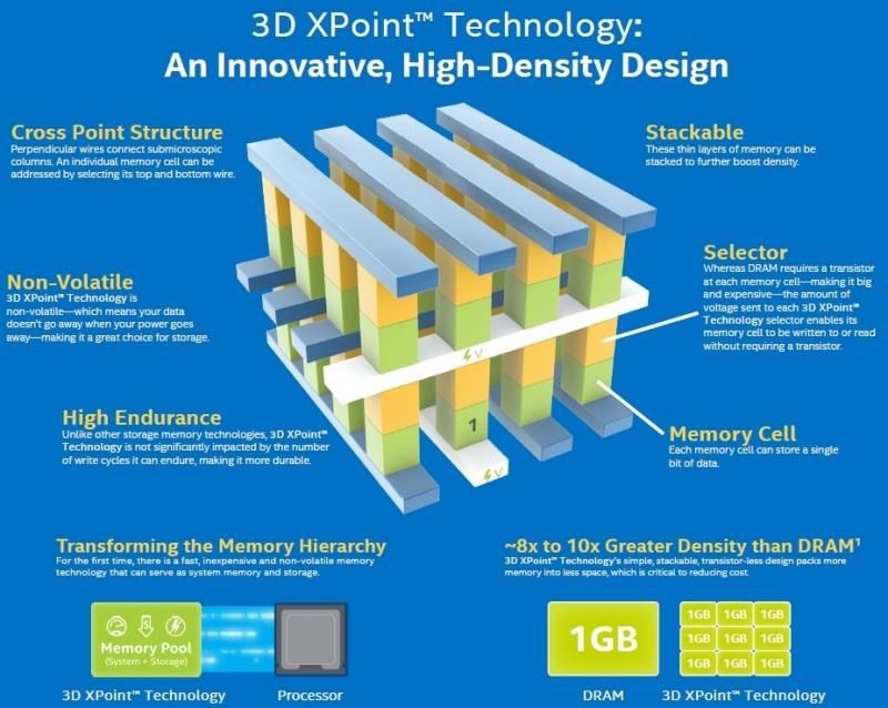
3 – Emerging memory technologies
 TOP ELECTRODE
PCRAM Technology
• Principe de fonc/onnement : changement de
 phase du volume ac/f de l’élément de PCM
 stockage de l’informa/on
 ACTIVE
 HEATER
 VOLUME
 ETAT RESET ETAT SET
 Phase amorphe • Ecriture: changement de phase
 Phase cristalline

• Lecture: contraste de résistance électrique induit par effet Joule sous
 l’applica/on d’une impulsion
 entre la phase amorphe et la phase
 électrique
 cristalline. intensity
 RESET SET

 time
 temperature
 amorphisation crystallisation
 liquid
 Tmelting ~ 600°C
 nucleation
 and growth
 of crystals
 Tglass

 Initial Initial
 state state
 time
 ~ 10 ns ~ 100ns

 7-mars-17 28
3 – Emerging memory technologies
PCRAM Technology
• Mémoire non-vola8le (NVM)
• Temps d’accès court (12ns)
• Ecriture et effacement rapide (100ns)
• Tension de fonc8onnement basse (3V)
• Ra8o Roff/Ron important (x1000)
• Haute endurance (1012 cycles)
• Réten8on prouvée à 10 ans à 150°C y compris à
 température de soudage ! From Intel / Micron websites
• Intégra8on 2D démontrée dans une architecture
 crossbar pour applica8ons de stockage (cf. 3D XPoint)
• Technologie la plus mature parmi les candidates au
 remplacement de la flash (technologie industrielle)

Défis
• Dérive de résistance et courant de reset rela8vement haut affectent la mise à
 l’échelle de la cellule mémoire (élément de stockage et transistor de sélec8on)

 7-mars-17 29
3 – Emerging memory technologies
ReRAM Technology
Varia/on résistance d’une structure Métal\Isolant\Métal contrôlée électriquement
 2 Etats 2 Opéra/ons
 HRS à Haute résistance (Etat « 0 ») Set à passage de l’état HRS à LRS
 LRS à Basse résistance (Etat « 1 ») Reset à passage de l’état LRS à HRS

 Métal RESET Métal

 LRSIsolant SET HRS
 Isolant

 Métal Métal
 Oxide-base RAM (OxRAM) Conduc/ve Bridge RAM (CBRAM)
 Filament conducteur = chaine d’atomes
 Filament conducteur = chaine de lacunes métalliques (Ag, Cu)
 d’oxygène (migra/on)

 Switching filamentaire unidimensionnel dans les 2 cas

 7-mars-17 30
3 – Emerging memory technologies
ReRAM Technology

AVANTAGES INCONVENIENTS
• Structure simple, facile à fabriquer • Etape ini8ale de forming à plus
• Fort poten8el pour la réduc8on de haute tension pour créer le filament
 taille (mécanisme filamentaire)
 • Variabilité importante de l’état HRS
• Faible tension (1V – 3V)
• Courants de programma8on 10-100µA
• Vitesse de commuta8on < 100ns
• Coût énergé8que ~ 100pJ/bit
• Endurance > 108 cycles (OxRAM)
• Réten8on de l’informa8on
 > 10 ans à 70°C
• Intégra8on en BEOL à faible
 température mais aussi
 compa8ble FEOL (OxRAM)
• Des produits déjà démontrés
 7-mars-17 31
Emerging Technologies : Fe-RAM

 Shosuke F. et al., First demonstration and performance improvement of ferroelectric HfO2-based resistive switch with low
 operation current and intrinsic diode property, VLSI 2016

7-mars-17 Your Name / Affilia8on 32
Emerging Technologies : Fe-RAM
 Müller J et al. Ferroelectric hafnium oxide: a CMOS-
 compatible and highly scalable approach to future
 ferroelectric memories. IEDM 2013

 Pas un effet de chargement/
 déchargement dans l’oxyde de grille
 (variation contraire de la tension de
 seuil)

 Yurchuk et al., Charge-Trapping Phenomena in HfO2-Based
 FeFET-Type Nonvolatile Memories, IEEE Transaction on
 Electron Devices Vol. 63, No. 9, sept. 2016

 ++: consommation, rapidité
 --: cyclage, rétention

 Concept de mémoire non-volatile très récent, manque de maturité,
 démonstration d’intégration au nœud 28nm HKMG
 HfO2 ferroélectrique: utilisable aussi pour des transistors MOS à faible
 pente sous le seuil (concept de capacité négative de grille)

7-mars-17 Your Name / Affilia8on 33
3 – Emerging memory technologies : MRAM

• Conductance of magne8c metal plates is larger in
the presence of a magne8c field perpendicular to
the current flow William Thomson
 1824-1907

 (R. S. Popovic, 2004)

• Currently known as Anisotropic Magnetoresistance (AMR)
• Resistance varia8on a}ained: 2%-5% in RT
 34
3 – Emerging memory technologies : MRAM

 Peter Grünberg and Albert Fert
 2007 Nobel Prize in Physics

¢ Thin stacks of FM/NM metals have seen a conductance
 increase of up to 100% when subjected to a magne8c field

 B. Guinasch et al., 1989 M. N. Baibich et al., 1988

 35
SPIN TECHNOLOGY OVERVIEW
GIANT MAGNETORISTANCE
 Peter Grünberg and Albert Fert
 2007 Nobel Prize in Physics

 • In FM/NM/FM structures, electrons are sca}ered as a result
 of interac8ons between the magne8c field and their spin

 An8-Parallel configura8on
Spin-up Spin-down 36
SPIN TECHNOLOGY OVERVIEW
GIANT MAGNETORISTANCE
 Peter Grünberg and Albert Fert
 2007 Nobel Prize in Physics

 • In FM/NM/FM structures, electrons are sca}ered as a result
 of interac8ons between the magne8c field and their spin

 Hext

 Parallel configura8on
Spin-up Spin-down 37
3 – Emerging memory technologies : MRAM

 T. Miyazaki, J. Moodera, J. Slonczewski
 (not in the pictures: M. Jullière)

 ¢ Spin-Dependent Transport (SDT): spin-up and spin-down have
 different probabili8es of tunneling an FM/I/FM structure

 An8-parallel configura8on
Spin-up Spin-down 38
3 – Emerging memory technologies : MRAM

 T. Miyazaki, J. Moodera, J. Slonczewski
 (not in the pictures: M. Jullière)

 ¢ Spin-Dependent Transport (SDT): spin-up and spin-down have
 different probabili8es of tunneling an FM/I/FM structure

 Parallel configura8on
Spin-up Spin-down 39
3 – Emerging memory technologies : MRAM
 Field Induced Switching Current Induced Switching Voltage Induced Switching
 Writing current
 Magnetic field
 Writing current Magnetoelectric RAM
 (MeRAM)

 V+

 Toggle
 Spin Transfer
 ¢ First MRAM genera8on access
 Torque
 ¢ Two combined transistor ¢ No external magne8c field
 magne8c fields
 ¢ Spin polarized current
 Magnetic field V-
 Heating current
 access
 transistor

 ¢ Very low current
 ¢ Voltage-controlled magne8c
 Write path anisotropy effect
 access
 Thermally Assisted transistor
 access Spin Orbit
 Switching
transistor Torque
 ¢ Free layer blocked at room ¢ Three terminals
 temperature
 ¢ SOT switching not fully understood
 ¢ Heat current + magne8c field (Rashba effect + Spin Hall Effect)

 40
3 – Emerging memory technologies : MRAM

• Vitesse à l’écriture (~ns)
• Courant d’écriture ~5MA/cm² ó 15uA pour 20nm,
 diminue avec la surface de la MTJ
• Endurance (>1014-15 )
• Intégra/on sur CMOS
 • Tension d’écriture et résistance (~kΩ) compa8ble avec CMOS Magnetic
 • ~3 masques supplémentaires element level
 • Température back-end faible (
 immune aux radia/ons
• Compromis entre :
 • Vitesse et consomma8on à l’écriture
 • Réten8on et consomma8on à l’écriture
• Scalabilité assurée jusqu’à 14 nm
 • Stabilité propor8onnelle au volume
 • Courants d’écriture très pe8ts : risque d’écriture lors de la lecture

 41
3 – Emerging memory technologies : MRAM

 STT-MRAM Cache memory
 Everspins MRAM Arduino Shield

MRAM based memresistor – Human Brain – IEF/CEA Crocus MRAM flexible sensors

 42
3 – Emerging memory technologies : Overview

• All these technologies are Non-vola8le, based on
 resistance switching, with fast access 8me
• Two important aspects to consider
 • Technology maturity
 • Système integra8on (easy to replace actual memory)
 Metricx PCM OxRAM CBRAM PSTT MRAM FeFET Flash
 Endurance 4 4 2 5 1 3
 Energy 2 3 3 4 5 1
 Integra/on 3 5 4 2 5 3
 Scalability 4 5 5 4 3 1
 Reten/on 5 4 4 3 2 3
 Speed 4 3 3 5 4 1
 Maturité 3 3 2 2 1 5

 43
Techno overview summary

•J. Joshua Yang, Dmitri B. Strukov & Duncan R. Stewart
Nature Nanotechnology 8, 13–24 (2013)

 44
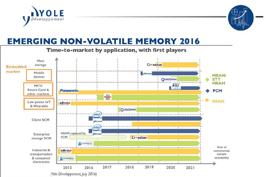
3 – Emerging memory technologies : Overview
• Actual market of emerging technologies is about 50 Millions $ - 80 billions for
 DRAM and Flash
• 2021: 4,6 billions $, a market growth of 110% per year
• All the majors semiconductors companies are leading this market – but lot of
 start-up too !

 Yole market report
 45
Summary

1 – Context and objec8ves of the lecture
2 – Classical technologies and memory architecture
overview (SRAM, DRAM, FLASH)
3 – Emerging memory technologies
4 – Compu8ng with Non-Vola8le memory technologies
 - For high performance compu8ng applica8ons
 - For Embedded applica8ons (Non-vola8le processor)
 - For secure applica8ons
5 - Conclusions

 46
Mo8va8on
• Solu/on MRAM
 PCRAM
 • Go towards non-vola8le systems using emerging NVMs FeRAM
 ReRAM
 • Current NVMs issues : Speed, Dynamic energy, Reliability
 …

 Cache NV Cache
 On-chip Embedded
 GPU Non-Volatile GPU
 CPU SRAM MRAM
 CPU

 High performance bus High performance bus

 Flash DDR Non-volatile Memory DDR
 eFPGA Controller Controller FPGA Controller Controller

 External Flash External DRAM External MRAM External MRAM

 Where and how to place MRAM to:
 reduce total power consumption ?
 keep same or get better performance ?
 47
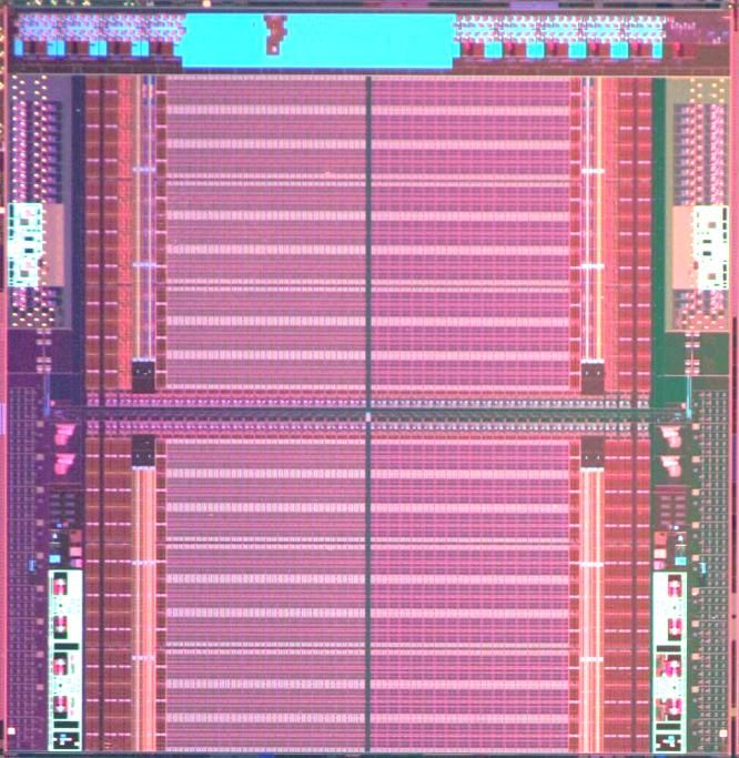
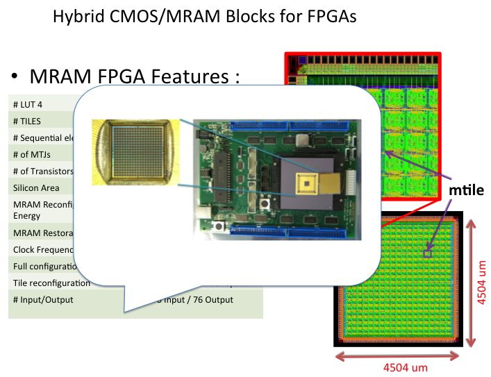
MRAM Research @ LIRMM

01/23/2015 48
Contribu8ons
1. Evalua8on of MRAM-based cache memory
 hierarchy:
 • Explora8on flow and extrac8on of memory ac8vity
 • L1 and L2 caches based on STT-MRAM and TAS-MRAM

2. Non-vola8le compu8ng
 • Instant-on/off capability for embedded processor
 • Analysis and valida8on of Rollback mechanism

3. Secure applica8ons with NVM

 49
MRAM applied to cache NV Cache On-Chip • Possible studies CPU SRAM High performance bus Performance comparison New architectures DDR 3D-Stacking Controller capability of ENERGY SPEED MRAM External DRAM NV Memory Logic layer Non-volatile Cache AREA Cache POTENTIAL APPLICATIONS ? ¢ SRAM vs MRAM fast (SRAM) Hybrid SRAM/ ¢ Benefits of MRAM Low leakage CPU Cache MRAM cache slow High density (MRAM) Non-vola8lity Take advantages of MRAM Mitigate drawbacks of MRAM Low leakage write latency High density write energy Non-volatility 50
MRAM applied to cache
 NVM exploration flow

 Benchmarks
 NVM memory array

 1. Define the architecture gem5* Memory Modeling (NVSim**, SPICE…)
 Latency Prototype
 Full-system simulator
 § Single/Multi-core
 2. Explore MRAM-based
 Architecture level cache configurations
 Circuit level
 § L1, L2, L3, Hybrid… Execu8on 8me
 # Reads / Writes
 3. Extract many useful information
 # Hits / Misses
 § Runtime, cache energy,
 cache transactions…
 Access energy
 Total L1/L2 energy consump8on Static power

* N. Binkert et al., “The gem5 simulator,” ACM SIGARCH Computer Architecture News, Aug. 2011.
** X. Dong et al., “NVSim: A Circuit-Level Performance, Energy, and Area Model for Emerging Nonvolatile Memory,” IEEE Transactions on Computer-Aided Design of Integrated Circuits and
Systems, Jul. 2012 .

 51
MRAM applied to cache
 Experimental setup
 From single to multi-core architecture
 ARMv7 ISA
 Private L1 instruction/Data
 Shared L2
 (Additional levels of caches possible)
 Main Memory

 Core Core Core
 1 2
 … N

 L1 I/D L1 I/D L1 I/D

 Shared L2
 45nm 45nm 130nm 120nm
 DDR3

 SRAM SRAM
STT-MRAM TAS-MRAM
 (Baseline) (Baseline)

 52
MRAM applied to cache
 Circuit-level analysis:
 Area Models (NVSim) & Prototype

 SRAM STT-MRAM

 100 512kB L2 32kB L1
 Node Technology
 (mm²) (mm²)
 10 SRAM 1.36 0.091
 45nm
Area (mm²)

 STT-MRAM 0.82 0.117
 1
 SRAM 9.7
 0,1 120nm -
 TAS-MRAM 11.7

 0,01
 8kB 16kB 32kB 64kB 128kB 256kB 512kB 1MB 2MB 4MB

 ¢ MRAM is denser for large cache capacity
 ¢ MRAM cell size smaller than that of SRAM
 ¢ MRAM needs large transistors for write
 ¢ TAS-MRAM cache larger due to field lines
 53
MRAM applied to cache
 Circuit-level analysis:
 Models (NVSim) & Prototype
 Read Write Standby
 Latency Energy Latency Energy Leakage
 Node Technology
 (ns) (nJ) (ns) (nJ) (mW)
 SRAM 4.28 0.27 2.87 0.02 320
 512kB 45nm /2.2 ≈ 2.1 2.5 /14
L2 cache STT-MRAM 2.61 0.28 6.25 0.05 23

 SRAM 5.95 1.05 4.14 0.08 82
 120nm /8
 TAS-MRAM 35 1.96 35 4.62 10

 STT-MRAM ≈ SRAM MRAM > SRAM MRAM SRAM

 Latency Energy Latency Energy Leakage
 Node Technology
 (ns) (nJ) (ns) (nJ) (mW)
 32kB
L1 cache SRAM 1.25 0.024 1.05 0.006 22
 45nm /7
 STT-MRAM 1.94 0.095 5.94 0.04 3.3
 MRAM > SRAM MRAM > SRAM MRAM
MRAM applied to cache
 Case study

• Quad-core architecture: Core Core Core Core
 1 2 3 4
 – Frequency 1GHz
 L1 I/D L1 I/D L1 I/D L1 I/D
 – ARMv7 ISA 32 kB 32 kB 32 kB 32 kB

 – Private L1 I/D
 Shared L2 512 kB
 – Shared L2
 – DDR3 Main memory DDR3 512 MB

• Benchmarks
 – SPLASH-2
 • Mostly high performance compu8ng
 – PARSEC
 • Anima8on, data mining, computer vision, media processing

 55
MRAM applied to cache
 Architecture-level analysis:
 gem5
Read/Write ratio L2/L1 access ratio

 Number of accesses
 Benchmark
 L1 cache L2 cache
 ~2 billions
 SPLASH-2 ~26 millions
 (0.5 billions/CPU)
 ~12 billions
 PARSEC ~16 millions
 (3 billions /CPU)

 Static/Dynamic energy ratio

 L2 à 90%
 Static energy
 L1 à 80%

 56
MRAM-based L2
 Execution time

 STT-MRAM L2 (45 nm) TAS-MRAM L2 (130 nm)
 Normalized execu8on 8me

 1,4 SRAM
 1,2 Baseline
 1
 0,8
 0,6
 0,4
 0,2
 0

• Observa8ons: barnes ocean2
 – STT shows good performance 100

 Cache miss rate (%)
 • L2 has small impact in overall performance 80

 – For TAS, 14% of penalty in average (SPLASH-2) 60

 • Depends on applica8ons 40
 (Cache miss rate, L1/L2 access ra8o) 20

 0
 Execu8on 8me

 57
MRAM-based L2
 Total L2 cache energy
 consumption

 STT-MRAM L2 (45 nm) TAS-MRAM L2 (130 nm) SRAM
 Baseline
 1,0
 Normalized L2 energy

 0,8
 0,6
 0,4
 0,2
 0,0

• Observa8ons:
 fluidanimate (read) fluidanimate (write)
 – Up to 90% of gain for STT

 Bandwidth (GigaBytes/s)
 radix (read) radix (write)
 – From 40% to 90% for TAS 1,6
 End of fluidanimate
 • Due to the very low leakage of MRAM-based cache 1,2
 End of radix
 0,8
 0,4
 0
 Execu8on 8me

 58
MRAM-based cache
 Summary

• NVM explora/on flow available
 – Input from models or silicon chip
 – Memory ac8vity analysis
• Is MRAM suitable for cache ?
 – Good candidate for lower level of cache (L2 or last level cache)
 • Up to 90% of energy gain
 • No or small performance penalty
 • More memory capacity using MRAM
 • Cache L2 is up of 20% energy consump8on of overall system
 – Not suitable for upper level of cache (L1) for high performance – but
 depending of the applica8on some gain in energy
 • Micro-architectural modifica8ons required to mask latency
 • Not detailed in this presenta8on but full evalua8on of cache L1 done too

 59
Contribu8ons

1. Evalua8on of MRAM-based cache memory
 hierarchy:
 • Explora8on flow and extrac8on of memory ac8vity
 • L1 and L2 caches based on STT-MRAM and TAS-MRAM

2. Non-vola8le compu8ng
 • Instant-on/off capability for embedded processor
 • Analysis and valida8on of Rollback mechanism

3. Secure applica8ons with NVM
 60
MRAM-based processor
Normally-off computing Cache
 Non-volatile
 On-Chip
 SRAM
 CPU

 High performance bus

• Two concepts: DDR
 Controller
 – Instant on/off
 • Restore processor External DRAM
 state

 – Backward error recovery
 (Rollback)
 • Restore previous valid state

 61
MRAM-based processor
 Fetch Decode Execute Memory Write back
 Instant on/off & Rollback
 Instruc8on NV Data NV
 Register
 Register Reg

 ALU
 bus bus Reg
 file
 file

 Address decoder Address decoder

 Instruc8on Data
 Non-vola8le register
 Cache Cache
 +
 Non-vola8le Memory
 Memory bus interface Memory bus interface

 +
 Checkpoint Memory (Rollback)
 MRAM
 Main memory
 MRAM-based register

 Write driver (lev)

 MRAM CMOS FF Read
 Main memory
 (Checkpoint Memory)
 Write driver (right)

 Layout of NV Flip-Flop
 (28nm FDSOI, 90nm STT)

B. Jovanovic, R. Brum, L. Torres, Comparative Analysis of MTJ/CMOS Hybrid Cells based
on TAS and In-plane STT Magnetic Tunnel Junctions, IEEE Transactions on Magnetic,, 2014. 62
MRAM-based processor
 Case study: Amber 23 processor
 (ARM based instruction)
 3-stage pipeline FEATURES
 Fetch Decode Execute

Instruc8on Register

 ALU
 bus file • 3-stage pipeline
 • 16x32-bit register file
 Pipeline registers • 32-bit wishbone system bus
 Address decoder • Unified instruction/data cache
 Unified Instruc/on/Data (16 kBytes)
 Cache • Write through
 Memory bus interface • Read-miss replacement policy
 • Main memory (> Mbytes)
 • Multiply and multiply-accumulate
 operations
 Main memory

Ø Implementation of both instant-on/off and rollback (Verilog code modified)

Ø Duplication of the registers to emulate the non-volatility
 63
Instant on/off
 Previous stage Next stage
 0

Instant on/off 1

 clk SAVE enable
 RESTORE
 clk
 Reg

1 Save the register’s state NV reg

 Main memory based on MRAM
2 POWER DOWN
 Data preserved
 Main memory based on MRAM
3 POWER UP
 Data available

 Previous stage Next stage
 0

 4
 1

 RESTORE clk SAVE enable
 clk
 Reg

Restore the register’s state NV reg

 64
Instant on/off
 Instant-on/off: backup energy

 ¢ 1644 Flip-Flops saved
 ¢ Flip-Flops are backed-up in parallel

 ¢ Backup energy:
 à less than 1nJ for STT-MRAM
 à less than 10nJ for TAS-MRAM

 ¢ [1] The required current to erase and
 program flash can vary from 4 to 12 mA

[1] “Benchmarking mcu power consumption for ultra-low-power applications,” White paper, Texas Instruments

 65
Instant on/off
 Instant-on/off: Restore energy

 ¢ 1644 Flip-Flops restored
 ¢ Flip-Flops are restored in parallel

 ¢ Restore energy:
 à 20pJ for both STT-MRAM and TAS-
 MRAM
 ¢ [1] Wang et al. showed that the energy
 consump8on to restore 1607 Flip-Flops
 from off-chip flash (on-chip flash) is
 1.3µJ (0.6µJ)
[1] “A 3us wake-up time nonvolatile processor based on ferroelectric flip-flops,” in ESSCIRC (ESSCIRC),
Proceedings of the. IEEE, 2012
 66
Instant on/off
 Instant-on/off: sleep mode

 Without instant-on/off With instant-on/off

Minimum Tsleep required to be
 more energy efficient

 67
Instant on/off
 Instant-on/off: sleep mode
 Switching activity à 0.5/cycle

 Synthesis of the Amber 23 Pactive = 173 mW (40 MHz)
(65nm CMOS low-power HVT process) Pleakage = 12 mW

 Technology Minimum Tsleep
 STT-MRAM 130 ns
 TAS-MRAM 968 ns
 OxRAM 4.9 µs
 PCRAM 69 µs

 • Not considering the power down/up circuitry
 • Cache warm-up penalty to consider
 • Area overhead to consider
 68
Rollback
 ON OFF
 Rollback NORMAL EXECUTION
 Main Checkpoint
 memory memory
 - Only the main memory contents are modified
 - The checkpoint memory is powered off

 Previous
 ON Save ON
 0 Next stage
 stage
CHECKPOINT

 = +
 1

 RESTORE clk SAVE enable Main Checkpoint
- Save registers Reg clk memory memory
- Save memory NV reg

 ON Restore ON
ROLLBACK Previous
 stage
 0 Next stage

 +
 1

 SAVE
 Main Checkpoint
1. Stall the processor RESTORE clk enable
 memory memory
 clk
2. Restore checkpoint Reg
 NV reg
3. Execution

 69
Rollback
 Rollback
 Buffer (128 entries)

(Memory part) Address
 NORMAL EXECUTION
 Main Checkpoint
 - Only the main memory contents are modified memory memory
 - Buffer to save addresses of modified memory locations

 ON OFF
 CHECKPOINT ROLLBACK
 - Only the modified memory locations are copied - Only the modified memory locations are restored

 Buffer (128 entries) Buffer (128 entries)

 Main Checkpoint Main Checkpoint
 memory memory memory memory

 ON Save ON ON Restore ON

 70
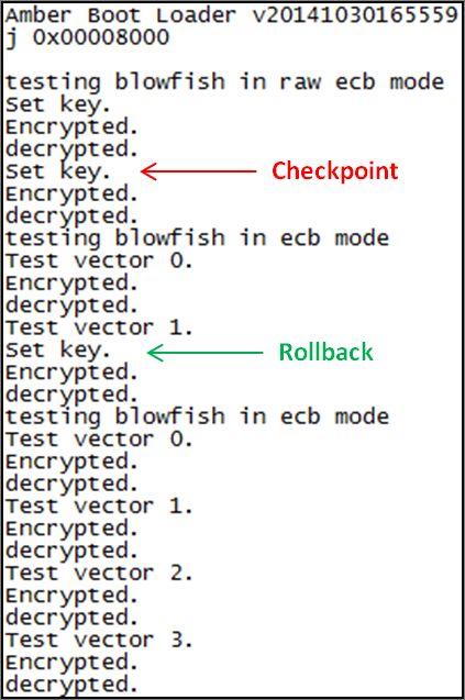
Rollback
 Rollback: validation (b)

 (a)

 Fig. 12: Validation of the rollback capability (terminal outputs of the blowfish applica-
 tion)
 Checkpoint
created here

 …
 Checkpoint
restored here
 Fig. 13: Checkpoint count for different address buffer size (blowfish application)

 ACM Transactions on Embedded Computing Systems, Vol. 9, No. 4, Article 39, Publication date: March 2010.

 71
Rollback
 Rollback: validation

 • Dhrystone 2.1 applica8on
 Checkpoint
created here • Register part:
 – Same 8me/energy as intant-on/
 off to backup/restore
 – Area overhead to consider

 … • Memory part:
 – To be evaluated more precisely
 Checkpoint – We know how to evaluate
restored here
 checkpoint memory size
 – Penalty due to cache warm-up to
 consider

 72
Summary

 Instant-on/off & Rollback
 Architectural changes

 73
Contribu8ons

1. Evalua8on of MRAM-based cache memory
 hierarchy:
 • Explora8on flow and extrac8on of memory ac8vity
 • L1 and L2 caches based on STT-MRAM and TAS-MRAM

2. Non-vola8le compu8ng
 • Instant-on/off capability for embedded processor
 • Analysis and valida8on of Rollback mechanism

3. Secure applica8ons with NVM
 74
WHAT ABOUT SECURITY …
 Akio Fukushima*, Takayuki Seki, Kay Yakushiji, Hitoshi Kubota, Hiroshi Imamura, Shinji Yuasa, and Koji Ando
 National Institute of Advanced Industrial Science and Technology (AIST), Spintronics Research Center, Tsukuba, Ibaraki 305-8568, Japan
 E-mail: akio.fukushima@aist.go.jp
 Received May 23, 2014; accepted July 7, 2014; published online July 25, 2014

 Generation of practical random numbers (RNs) by a spintronics-based, scalable truly RN generator called “spin dice” was demonstrated. The
 generator utilizes the stochastic nature of spin-torque switching in a magnetic tunnel junction (MTJ) to generate RNs. We fabricated eight
 perpendicularly magnetized MTJs on a single-board circuit and generated eight sequences of RNs simultaneously. The sequences of RNs of
 True Number
 Smart Efficient TRNG
 different MTJs were not correlated with each other, and performing an exclusive OR (XOR) operation among them improved the quality of the RNs.

 Generator The RNs obtained by performing a nested XOR operation passed the statistical test of NIST SP-800 with the appropriate pass rate.

 based on MRAM
 © 2014 The Japan Society of Applied Physics

 R
 andom numbers (RNs) are a fundamental building
 Pulse circuit
 block of modern cryptographic systems. Much effort MgO-cap Electrode
 Physically has been devoted to developing better random
 Physically Unclonable
 number generators (RNGs). Taxonomically, RNGs can be
 FeB
 or
 Unclonable
 categorized into two distinct groups: pseudo-RNGs (PRNGs) MgO-barrier
 Free

 Func8on
 Function using MRAM
 and truly RNGs (TRNGs). PRNGs are implemented in CoPt/Ru/CoPt Reference
 Random bit
 software and use deterministic algorithms to generate a
 STT-MRAM-Based PUF Architecture exploiting Magnetic Tunnel Junction Fabrication-Induced Variability

 Electrode
 no dedicated circuit technique is needed to implement our solution. The schematic
 sequence of RNs. They require seeds of RNs and will always representation of our design is shown in Fig. 7. Here, we emphasize the active cells
 and the reference cells sets. The number of active cells in our memory array is
 generate the same sequence of RNs from the same seed.
 Fukushima & al (2015)
 # = # ∙ # , where #Ar represents the number of rows (i.e., number of Word
 Lines), while #Ac represents the number of columns (i.e. number of Bit/Source Lines
 Thus, they are considered to be cryptographically insecure. Fig. 1. Schematic diagram of spin dice. A current pulse was injected into a
 in our array.
 For highly secure data encryption we need TRNGs, which are p-MTJ to switch the magnetization in the free
 #Ac Columns layer by STT. The magnetic
 Active Cells

 Dedicated logic for secure
 implemented in hardware and generate a sequence of RNs
Secure elements
 configuration of the p-MTJ was observed by measuring the resistance and
 converted into A0an RB by a comparator.

 Address Decoder
 using a nondeterministic physical event such as transmission #Rc Columns Reference Cells

 Elements based on MRAM

 #Ar Rows
 A1

 of a photon through a half mirror,1) chaotic fluctuation of

 …

 #Rr Rows
 An

 a semiconductor laser,2–6) or flux transmission in a single MTJs) integrated on a single-board circuit. We show that
 flux quantum device.7) However, all of these TRNGs have temperature compensation for switching probability could
 An+1
 a drawback in scalability, which is important for a system be easily achieved by adjusting the amplitude of the current
 An+2 Address Decoder
 Read / Write Selector

 …
 expected to handle a growing amount of data securely. pulse. We also show that the quality
 Am
 I I of RNs could be im-
 R Ref

 Side Channel
 Since 2007, we have been studying a spintronics-based proved by performing an XOR operation on those generated
 Sense Enable

 Side Channel Analysis
 WD SA

 TRNG referred to as “spin dice”,8–10) in which binary RNs or
 Analysis by different p-MTJs. We evaluated the quality of the RNs by
 DATA_IN

 Fig. 7. Schematic representation of our PUF solution implementation
 DATA_OUT

 of MRAM memories
 random bits (RBs) are generated by using the stochastic using the statistical test suite NIST SP-80018) and confirmed
 In all case studies, for simplicity, we have used square memory arrays, so # = #
 nature of spin-transfer-torque (STT) switching11–15) in mag- that they were
 However, practical Vatajelu
 truly RNs.
 this is not a requirement
 & al (2015)
 for viable PUF implementation. Depending on the
 application and/or allowed area, different ratios can be chosen. The number o
 netic tunnel junctions (MTJs). The basic mechanism for Figure 1reference
 shows cellsthein theschematic
 implementationdiagram of where
 is # = # ∙ # , spin#Rcdice. Thethe
 represents
 number of columns (i.e., the number of MTJ devices connected in series), and #Rr
 generation of an RB is the same as that for writing a data bit film stack represents
 of the the p-MTJ number consisted
 of rows (i.e., the ofnumber of branches of75
 the following: a 2-nm-
 series MTJ). The
ultra-low-voltage operation.
 2014
 W HAT ABOUTIt SECURITY
d, scalable truly RN generator called “spin dice” was demonstrated. The
 is known that thermal agitation True … causesNumber the switching
 field of a small magnet to (a)have a distribution.20) Similarly,
 magnetic tunnel junction (MTJ) to generate RNs. We fabricated eight Generator
ated eight sequences of RNs simultaneously. The sequences of RNs of the switching current of a p-MTJ nano-pillar also has a
xclusive OR (XOR) operation among them improved the quality of the RNs.
 statistical test of NIST SP-800 with the appropriate pass rate.
 distribution as a result of thermal agitation, which yields the
 Smart Efficient TRNG based on perpendicular STT-MRAM
 switching probability expressed as21)
 ( " ! "2 # )
 Appl. Phys. Express 7,t 083001 (2014) I
 Pulse circuit
 P sw ðIÞ ¼ 1 $ exp $ exp $! 1 $ ; ð1Þ
 Table I. R for the raw!bits ·
 Ic0XOR
 0 and for after XOR, XOR , and 2
 fabricate
 3
 MgO-cap Electrode
 operations are performed. The mean values were obtained from 120 sets of
 will pro
 FeB where t is the1 ©duration
 10 bits. Errorsof
 9
 are the
 definedcurrent
 as «1·. pulse, ¸0 is the attempt numbers
 Free or
 MgO-barrier time, ¦ is the thermal stability parameter R · of the nanomagnet, ing cand
 Raw XOR XOR 2
 XOR suitable
 3

 CoPt/Ru/CoPt Reference
 Random bit
 and Ic0 is the MTJ1
 critical switching
 4.18 « 0.52
 (c) current at 0 K. enormou
 1.044 « 0.022
 In Fig. 2(c)MTJ2
 the switching
 3.95 « 0.40 probabilities P sw obtained from

 Psw
 Psw
 Electrode 1.000 « 0.009
 3
 4 © 10 switching events
 MTJ3 4.34 « 0.54
 are plotted
 1.029 « 0.026 as a function of current,
 MTJ4 4.76 « 0.30
 which is well MTJ5
 reproduced
 3.93 « 0.42 by Eq. (1) with ¸0 = 1 ns, t = 200
 1.001 « 0.011 1) T. Je
 Main principle
 Fig. 1. Schematic diagram of spin dice. A current pulse was injected into a 1.030 « 0.021 Rev.
 p-MTJ to switch the magnetization in the free layer by A.
 STT.Fukushima
 The magneticet al.
 ns, ¦ = 109, and
 MTJ6 I4.29=
 c0 « 0.30 0.96 mA. As 0.998 shown« 0.010
 in Fig. 2(c), P
 2) sw
 A. U
 configuration of the p-MTJ was observed by measuring the resistance and MTJ7 3.65 « 0.41 Oow

 converted into an RB Rby a comparator.
 gradually increases with increasing
 MTJ8 4.68 « 0.44
 1.028 « 0.015 current from I = 0.7 to Nat.
 R R R R 3) I. Re
 0.8 mA, which enables us to precisely control Psw by altering 0241
 I I I I I 4) I. Ka
 I 0 0 0 0 0 the current. The temperature dependence of Psw at I = 0.73 4, 58
 MTJs) integrated
 (a) on a single-board
 (b) (c) circuit. We(d) show (e)that 18)
 5H
 temperature compensation for switching probability could
 0 mA is shown Table II. Pass rate of the randomness tests of NIST SP-800.
 Fig.in2.Fig.Switching2(d). At properties
 each temperature, of the 2 © 10(a)
 p-MTJ.
 5) K.
 Yosh
 Pass rate
 be easily achieved by adjusting the amplitude
 Time
 of the current switching events
 field. (b)wereResistance
 measured
 Raw
 to
 versus
 XOR 2obtain P . One
 current.
 XOR sw XOR
 3 (c) P can see 5512
 sw 6)vers
 X. L
 Excite pulse
 pulse.
 Reset pulse
 We also show that the quality of RNs could be im-
 P state 50% that Psw exhibits good linearity
 dependence
 MTJ1 of Psw. between
 0.000
 0.000
 29 and 38 °C with Supe a
 7) T. Su

 proved by performing an XOR operation on those generated ¹1
 slope of 0.037 °C . Therefore, the change
 MTJ2 0.000
 0.417in Psw caused by
 8) A. F
 Paten
 by different p-MTJs. We evaluated 100%
 the quality of the RNs by MTJ3 0.000
 the temperatureMTJ4 variation 0.000of «10 °C can be easily compen-
 0.167 9) A. F
 using the statistical test suite NIST SP-80018) and confirmed 0.467 Ext.
 sated for by varying
 MTJ5 the0.000
 current 0.058 by % &30 µA. 10) S. Yu
 that they were practical truly RNs.
 AP state 50%
 practically
 MTJ6 at zero magnetic field. TheH. Kr
 0.000
 Figure 1 shows the schematic diagram of spin dice. The Figure 3 schematically shows the procedure 0.475 for the rolling Bone
 Initial state
 AP
 of the spin dice.
 states
 MTJ7 were
 0.000 212 and 411 ³, respe Nom
 film stack of the p-MTJ consisted of the following: a 2-nm- MTJ8The AP 0.000 and P states in the p-MTJ 11)are
 0.075
 J. C.
 thick FeB magnetic free layer with a MgO cap layer, a 1-nm- Fig. 2(b), the P to AP
 assigned to the binary values “0” and “1”, respectively. 13) (AP to P) swit
 12)
 The
 L. B
 F. J.
 thick
Fig.
 Akio3. MgO barrier,
 Spin dice
 Fukushima*, and Reset
 process. a CoPt/Ru/CoPt
 Takayuki and excite pulsesreference
 Seki, Kay Yakushiji, layer.
 are applied The
 sequentially.
 Hitoshi at aShinji
 Kubota, Hiroshi Imamura, current
 Yuasa, and of Koji0.75Ando mA Spin (¹0.27
 dice: A mA), Phys
 film wastruly
 scalable fabricated
 random into a pillargenerator
 number shape by based
 a combination of
 on spintronics, Applied Physics Express 7,is083001
 of 0.590 that (2014)
 obtained for an infinite number of RBs. They 76 0830
 14) J. Z.
 160 mV (¹110 mV). The fact that the r Abra
WHAT ABOUT SECURITY … True Number
 Generator
Smart Efficient TRNG based on perpendicular STT-MRAM
(instead current pulse, external field is used) 50 Millions of random bits

 TRNG
 MRAM
 source 1
 Random
 number

 MRAM
 source 2

 Correc8on TRNG Output

 MRAM
 source n

 77

Experiment done with IEF, Thibault DEVOLDER NIST Test
WHAT ABOUT SECURITY …
 Secure elements

 • Non-Vola8lity help security (and also Energy !)
 • Persistent data storage
 • Authen8ca8on
 • Ba}ery backed-memories
 • Secure CPU Boot

 NV – SRAM Non-Volatile SRAM/MRAM cell
 2 NV state
 1 Volatile State

 Read speed 39 ps (1.5 f) Density 25.000nm2/3bits

 Read Energy 5.8 fJ SNM 314 mV

 Write Energy 56 fJ DR Yes (1)

 Sta/c Power 396 nW WVD Yes (1)

B. Jovanovic, R. Brum, L. Torres, Comparative Analysis of MTJ/CMOS Hybrid Cells based on TAS
and In-plane STT Magnetic Tunnel Junctions, IEEE Transactions on Magnetic, 78
WHAT ABOUT SECURITY …
 Secure elements

 • Non-Vola8lity help security (and also Energy !)
 • Persistent data storage
 • Authen8ca8on
 • Ba}ery backed-memories
 • Secure CPU Boot
 • ….

 Non-Volatile SRAM/MRAM cell

 • First evalua8on of NV CPU @ LIRMM : Cache
 • 32-bit RISC like processor memory

 • Valida8on of checkpoint/rollback capability
 NV Memory
 • Non-Vola8le register bank (instead Vola8le)
 CPU
 • Low performance overhead Registers
 • Non-vola8le memory from register level to main memory NV Registers
 (Checkpoint)

B. Jovanovic, R. Brum, L. Torres, Comparative Analysis of MTJ/CMOS Hybrid Cells based on TAS
and In-plane STT Magnetic Tunnel Junctions, IEEE Transactions on Magnetic, 79
WHAT ABOUT SECURITY …
 Secure elements

Magnetic Logic Unit Match In place

 XOR Function Authentication function/comparison

Symetric Cryptography à Elementary operations XOR, Substitution, Shift

 80
The high fabrication-induced variability affecting the electric characteristics of the
 MTJ device guarantees the unpredictability, HAT ABOUT W the SECURITY
 unclonability and the uniqueness Physically
 of …
 the PUF solution (as it is shown in Section 5). For a PUF solution to be useful,Unclonable it has
 toSTT-MRAM-Based
 be reproducible (see Section 2 for definition). This condition
 PUF Architecture exploiting Magnetic Tunnel Junction Fabrication-Induced Variability 39:11
 is met, if after Func8on
 each
 run of the
 no dedicated algorithm
 circuit technique is needed toon a same
 implement our solution. device,
 The schematic the obtained results match with high
PUF solution
 probability.
 representation exploits is shown inthe differential
 Since the MTJ and access transistor
 of our design Fig. 7. Here, we emphasize thesensing active cells during read operation,
 parameter values are set by
 and the reference cells sets. The number of active cells in our memory array is
based
 # = on read
 fabrication,
 # ∙ # , where
 thecurrent
 #Ar
 read current
 represents the comparison
 number of
 distribution
 rows (i.e., against
 number
 Lines), while #Ac represents the number of columns (i.e. number of Bit/Source Lines)
 of Word a reference
 (IR) and value.
 the reference current (Iref) drift in
 the
 in oursame
 array. way for one device operated under the same environmental conditions
 #Ac Columns Active Cells
 (temperature and voltage). This characteristic guarantees high reproducibility of the
 results. However, due to the unavoidable and unpredictable noise in the circuit, there
 Address Decoder

 A0 #Rc Columns Reference Cells

 is an uncertain sensing zone for the sense amplifier. The bits falling in this zone, i.e.
 #Ar Rows
 A1
 …

 #Rr Rows
 the bits for which |IR-Iref| is smaller than the sensing margin of the SA, can induce a
 An

 meta-stable state, which will be randomly stabilized to '0' or '1' depending on the
 noise in the circuit. These cells can be read randomly as '1' or '0' at different runs of
 An+1
 An+2 Address Decoder

 the algorithm, and I are denoted as nondeterministic active cells in Fig 4. The
 Read / Write Selector
 …

 Am
 I
 existence of these nondeterministic cells reduces the reproducibility of the PUF
 R Ref
 Sense Enable
 WD SA

 solution. DATA_IN DATA_OUT

 Fig. 7. Schematic representation of our PUF solution implementation

 In all Active
 case studies,
 cellsfor simplicity,
 Reference we have usedin  AP
 cells square mmemory arrays, so # = # .
 agnetization  (logic  ‘1’) Logic  ‘0’ Logic  ‘1’ Nondeterministic logic state
 However, this is not a requirement for viable PUF implementation. Depending on the
 application and/or allowed 80 area, different ratios can be chosen. The number of80
 # of occurrences
 # of occurrences

 reference cells in the implementation is # = # ∙ # , where #Rc represents IR the
 number of columns (i.e., 60 the number of MTJ devices connected in series),
 represents the number of rows (i.e., the number of branches of series
 and #Rr60
 I refMTJ). The ‘1’ ‘0’
 equivalent resistance is given
 40 by equation (5): 40
 1 1 2 3
 20   =   ∑# 1 (5) 20
 ∑#
 0
 with RMTJ-i being the resistance of7the i-th MTJ 0
 8 device on 9 a row, for10 = 1: # .11In our 7 8 9 10 11
 case study, = , since the first step of theI proposed
 [A] PUF implementation
 x 10
 -5 I [A] -5
 x 10
 requires all reference cells be set to '1'. Ideally, we target an equivalent resistance
 Fig.
 =4. The
 so theimplementation
 reference current Iref bestrategy
 equal to the ofnominal
 the proposed
 current for read PUF '1' solution: 1) Write all cells to '1'; 2) Read each cell;
 operation ( ). This condition is achieved if and only if the number 3) Use the read value
 of rows equals the
 number of columns in our reference cells array, i.e., # = # . This is mandatory
 both for our implementation and for when the circuit is used as memory block.
ElenaHowever,
 Ioana Vatajelu,
 when theGiorgio Di used
 Natale, Mario Barbareschi, Lionel Torres, Marco Indaco, Paolo Prinetto STT-MRAM-Based PUF Architecture exploiting
 In the next section we describe the simulation set-up and demonstrate the viability of
Magnetic Tunnel
 required
 circuit is
 Junction
 to be
 as memory
 = ( + Fabrication-Induced
 block, the equivalent
 )/2 (as explained is Section Variability,
 resistance
 ACMreliable
 3) to guarantee JETC,read
 is
 2015 81
You can also read