Gate-on-Drain Overlapped L-Shaped Channel Tunnel FET as Label-Free Biosensor
←
→
Page content transcription
If your browser does not render page correctly, please read the page content below
Silicon
https://doi.org/10.1007/s12633-021-01285-z

    ORIGINAL PAPER

Gate-on-Drain Overlapped L-Shaped Channel Tunnel FET
as Label-Free Biosensor
Suman Das 1 & Bikash Sharma 1

Received: 22 April 2021 / Accepted: 19 July 2021
# Springer Nature B.V. 2021

Abstract
In this work gate-on-drain L-shaped channel Tunnel FET is proposed to detect various biomolecules through label-free bio-
sensing detection technique. Biomolecules can be detected in the proposed structure through modulation of ambipolar current
between channel and drain. Modulation of ambipolar current is performed by extending gate over drain in order to create a gate to
drain overlap (cavity) by etching the specific portion of the gate. Trapped biomolecules within cavity gets immobilized.
Immobilized biomolecules change the drain to channel tunneling width, thus changing the ambiploar leakage current. Drain
doping and cavity length was fine-tuned to achieve better sensitivity in terms of ambipolar current and ambipolar knee voltage
shift with and without presence of biomolecules. A maximum sensitivity of 3.8 × 10⁷ is achieved for drain doping of 5 × 10¹⁹
donors/cm3 and cavity length of 60 nm. A high value of sensitivity is achieved for each biomolecules when drain doping ranged
from 1019 donors/cm3 to 5 × 10¹⁹ donors/cm3 and cavity length ranged between 40 nm to 50 nm. Effect of differently charged
biomolecules on sensitivity has also be structured.

Keywords Tunnel FET . Biosensor . Label free detection . Gate on drain overlap . Dielectric modulation . Ambipolar leakage

1 Introduction                                                             Tunnel FET (TFET) is one of the emerging devices which
                                                                       overwriting the conventional MOSFET as a biosensor due to
Detection of biomolecules using biosensor has become a fast-           its band to band tunneling mechanism. It is overcoming the
growing field of study in present COVID 19 pandemic situa-             issue of sub-60 mV/decade subthreshold swing for MOSFET
tion. It creates enormous research interest among researchers          at room temperature and also TFET emerging as a promising
to discover different approach to detect the biomolecules. Lots        candidate for various sensing application [11–16]. Dielectric
of attempt has been made to make biosensor [1, 2]. Field effect        modulated TFET with various structures [6–9, 11–16] have
transistor (FET) based biosensors (bio-FET) [3–11] are mostly          been reported since last decades which is able to produce
drawing attention for its label free detection of biomolecules.        higher sensitivity. The higher sensitivity in biosensors means
The existence of biomolecules in free air change the properties
of bio-FET such as current, threshold voltage, subthreshold
swing, transconductance, etc. Apart from these advantages,
bio-FET is compatible with CMOS technology which support
system on chip configurations, smaller dimensions and used
to detect biomolecules from the air, making change in channel
conductance.

* Bikash Sharma
  ju.bikash@gmail.com

1
     Department of Electronics and Communication Engineering, Sikkim
     Manipal Institute of Technology, Sikkim Manipal University,       Fig. 1 Schematic of gate-on-drain overlapped L-shaped channel TFET
     Sikkim 737136, India                                              (GDOL-TFET)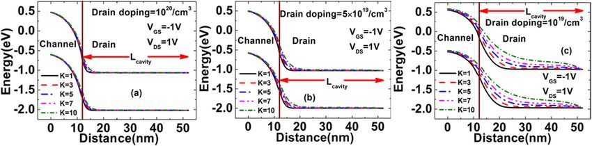
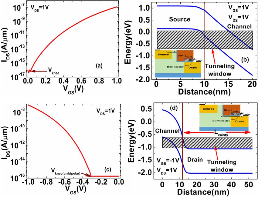
Silicon

Fig. 2 (a) ON state drain current
of GDOL-TFET at VDS = 1 V (b)
Energy band profile of source
channel junction at VGS = 1 V and
VDS = 1 V. (c) OFF state drain
current of GDOL-TFET at
VDS = 1 V (d) Energy band
profile of channel drain junction
at VGS = -1 V and VDS = 1 V

detectability of various biomolecules from air with a small                 channel to drain at negative gate voltage by extending gate
change in electrical parameters. Lots of attempt has been made              over drain thus making a cavity to trap the biomolecules.
to increase the sensitivity of TFET based biosensor using ei-               Various studies have been carried out to reduce the ambipolar
ther by material engineering or modulating the device struc-                leakage by overlapping gate on drain and increasing the di-
ture. Most of the results reported by various authors based on              electric constant of gate on drain overlap region [19]. Overlap
drain current modulation for different biomolecules at positive             between gate and drain, widens the tunneling barrier width at
gate voltage. In this literature an attempt has been made to                the channel-drain interface at negative gate voltages, which
design a silicon-based L-shaped channel TFET, following                     modulate the ambipolar current. In this manuscript for the first
the experimental structure reported by Kim et al. [17], at state            time a gate-on-drain overlapped L-shaped channel TFET
of art technology node [18]. Sensing of biomolecules have                   (GDOL-TFET) has been reported to sense different biomole-
been achieved by modulating the ambipolar current between                   cules having dielectric constant between K = 1 to 10 which

Fig. 3 Variation of ambipolar leakage current w.r.t. drain doping (a) ND = 1020 donors/cm3 (b) ND = 7 × 10¹⁹ donors/cm3 (c) ND = 5 × 10¹⁹ donors/cm3
(d) ND = 3 × 10¹⁹ donors/cm3 (e) ND = 1019 donors/cm3 for different biomolecules
Silicon

Fig. 4 Energy band diagrams of drain channel interface at different drain doping (a) ND = 1020 donors/cm3 (b) ND = 5 × 10¹⁹ donors/cm3 (c) ND = 1019
donors/cm3 for different biomolecules

works on the phenomenon of reduction in ambipolar current                        source voltage (VGS) greater than the knee voltage (Vknee) of
due to gate to drain overlap.                                                    the device. Vknee is the minimum gate to source voltage re-
                                                                                 quired for the device to enter into sub-threshold region. At
                                                                                 VGS > Vknee the energy band of channel region start to bend
                                                                                 and the valance band of source start to overlap with the con-
2 Device Structure, Operating Principle                                          duction band of channel thus creating a tunneling window,
and Simulation Setup                                                             which will be responsible for electron flow from source to
                                                                                 channel. This band to band tunneling depends on the tunnel-
The schematic of gate-on-drain overlapped L-shaped TFET
                                                                                 ing width and tunneling area of the tunneling junction be-
(GDOL-TFET) is shown in Fig. 1. Here an L shaped channel
                                                                                 tween source to channel. Tunneling junction area depends
device structure is taken into consideration due to its vertical
                                                                                 on the gate to source overlap and width of the vertical channel
tunneling mechanism from source to channel which in turns
                                                                                 (Wch) region. After tunneling, electrons will accumulate in the
increasing the band to band tunneling current rather than lat-
                                                                                 channel-oxide interface which will be swept away by the drain
eral tunneling device structures. The gate length is considered
                                                                                 voltage to the drain region thus rising a drain current between
as 13 nm based on latest technology roadmap. The width of
                                                                                 drain to source. The drain current and its corresponding ener-
channel (Wch) and thickness of oxide (SiO2) are considered as
                                                                                 gy band diagram is shown in Fig. 2(a) and (b) which defines
10 nm and 0.6 nm respectively. The work function of gate
                                                                                 the operation.
metal is chosen as 4.1 eV. One cavity is created to immobilize
                                                                                    But the main concern with this structure is the ambipolar
the biomolecules between gate and drain, which have length
                                                                                 leakage which generate at positive VDS and negative VGS. At
Lcavity = 40 nm and height Hcavity = 10 nm respectively. This
                                                                                 negative VGS the energy band of channel under gate region
cavity is used to decrease the ambipolar leakage current as
                                                                                 will move upward and at positive VDS the energy band of
well as is used to detect the biomolecules. A 0.6 nm thick
                                                                                 drain region will move downward. At a particular gate bias,
SiO2 is introduced throughout cavity to minimize the leakage
                                                                                 VGS=Vknee(ambipolar) the valance band of channel start to over-
current as well as uniform doping concentration of P+ source,
                                                                                 lap conduction band of drain as a result electron start to tunnel
N channel and N+ drain are considered with doping concen-
                                                                                 through the tunneling window and a tunneling current can be
tration of 1020 acceptors/cm3, 1017 donors/cm3 and 1020 ac-
                                                                                 obtained which is undesirable for digital circuit application
ceptors/cm3 respectively.
                                                                                 where leakage current should be minimum. The drain current
    The operation of the device is shown in Fig. 1. The opera-
                                                                                 and its corresponding energy band diagram is shown in Fig.
tion depends on vertical electron tunneling from the valance
                                                                                 2(c) and (d) which state the operation.
band of source to the conduction band of channel at gate to

Table 1   Variation of I Air I dielectric for different biomolecules (K = 1 to 10) at different drain doping, ND (/cm3). Lcavity is considered as 40 nm
                                           I Air
Drain doping, ND(/cm3)                             I dielectric

                                           K=1                      K=3                      K=5                      K=7                           K=10

1019                                       1                        150                      7857                     2×10⁵                         1.55×10⁶
3×10¹⁹                                     1                        120                      7100                     1.95×10⁵                      2.23×10⁷
5×10¹⁹                                     1                        100                      6700                     1.86×10⁵                      2.07×10⁷
7×10¹⁹                                     1                         90                      6100                     1.79×10⁵                      1.95×10⁷
1020                                       1                         80                      5600                     1.7×10⁵                       1.7×10⁶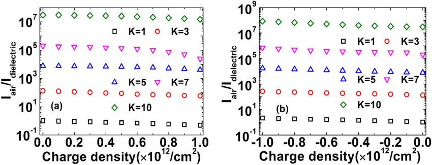
Silicon

Table 2 Variation of Vknee for different biomolecules (K = 1 to 10) at              method to reduce the ambipolar leakage is overlapping the
different drain doping, ND (/cm3). Lcavity is considered as 40 nm
                                                                                    gate on drain [19]. Overlap between gate and drain increases
Drain doping, ND(/cm3)        Vknee                                                 the capacitive coupling between gate and drain thus reducing
                                                                                    the ambipolar current. Gate on drain overlapped tunnel FET as
                              K=1              K=3    K=5     K=7      K=10         bio sensing application was first reported by abdi. et al. [24].
1019                          0                0.13   0.26    0.42     0.54
                                                                                    But here for the first time gate-on-drain overlapped method is
                                                                                    applied to L-shaped tunnel FET for bio sensing application.
3×10¹⁹                        0                0.09   0.19    0.31     0.56
                                                                                        Different biomolecules have different dielectric constant.
5×10¹⁹                        0                0.07   0.16    0.26     0.48
                                                                                    Based on this fact cavity is filled with different biomolecules
7×10¹⁹                        0                0.04   0.14    0.24     0.32
                                                                                    with different dielectric constant and ambipolar current is
1020                          0                0.05   0.13    0.22     0.29
                                                                                    measured each time. Sensitivity of this device is obtained by
                                                                                    i) ID,air/ID,biomolecules where ID,air is the ambipolar current when
                                                                                    cavity is filled with air and ID,biomolecules is the ambipolar drain
    All simulation results are obtained by Silvaco Atlas, ver-                      current when cavity is filled with biomolecules ii)
sion 3.20.2.R [20]. Non-local band to band tunneling are taken                      Vknee,ambiploar shift between Vknee,ambiploar of air in cavity and
into account to obtain the band to band tunneling between                           Vknee,ambiploar of biomolecules in cavity. Results section is
source to channel. To incorporate mobility effect concentra-                        divided with three portions viz. i) Optimization of drain dop-
tion dependent mobility model and CVT Lombardi model are                            ing w.r.t sensitivity ii) Optimization of cavity length w.r.t sen-
triggered. Due to high doping in source and drain region band                       sitivity. iii) Effect of positive and negative charged biomole-
gap narrowing model is enabled. To get the recombination                            cules in cavity.
effect Shockley-Read-Hall recombination is used with
Fermi-Dirac distribution statistics.                                                3.1 Optimization of Drain Doping

                                                                                    Doping concentration of drain region influence the sensitivity
                                                                                    of GDOL-TFET as biosensor. Figure 3 shows the variation of
3 Results and Discussions                                                           ambipolar leakage current for different drain doping under the
                                                                                    influence of different biomolecules in cavity. Dielectric con-
Minimization of ambipolar leakage current was carried out by                        stant of biomolecules are taken as K = 1, 3, 5,7,10. From Fig.
different authors in last decade [21–23]. Out of which one                          3(a) one can notice that as the dielectric constant is increasing,

Fig. 5 Variation of sensitivity at
different drain doping for
different biomolecules (a)
sensitivity w.r.t. current (b)
sensitivity w.r.t. knee voltage
shift. Lcavity is considered as
40 nm

Table 3   Variation of I Air I dielectric for different biomolecules (K = 1 to 10) at different length of cavity, Lcavity. Drain doping, ND is taken as 5 × 10¹⁹/cm3
                             I Air
Lcavity                              I dielectric
(nm)
                             K=1                             K=3                        K=5                           K=7                                K=10

40                           1                               100                        6700                          1.86×10⁵                           2.07×10⁷
50                           1                               133                        7800                          2.02×10⁵                           3.05×10⁷
60                           1                               171                        8600                          2.2×10⁵                            3.87×10⁷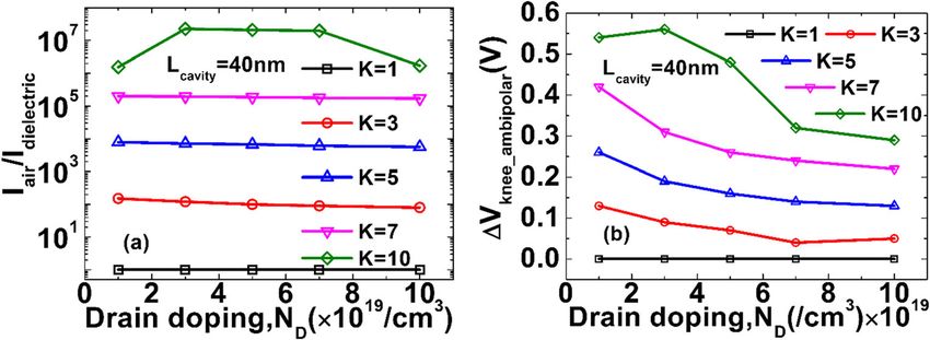
Silicon

Table 4 Variation of Vknee for different biomolecules (K = 1 to 10) at          Tables 1 and 2. From Fig. 5(a) and Table 1 it is clear that for
different length of cavity, Lcavity. Drain doping, ND is taken as 5 × 10¹⁹/
                                                                                highly doped drain region the sensitivity is less for a particular
cm3
                                                                                value of K. When doping is decreased the sensitivity is in-
Lcavity        Vknee                                                            creasing. Highest sensitivity is achieved for K = 10 and drain
(nm)                                                                            doping = 3 × 10¹⁹ donors/cm3. From Fig. 5(b) and Table 2 the
               K=1           K=3         K=5          K=7           K=10
                                                                                same trend is noticed throughout the range of K. For low
40             0             0.07        0.16         0.26          0.48        doped drain the Vknee(ambipolar) shift is high whereas for high
50             0             0.09        0.19         0.31          0.57        doping Vknee(ambipolar) shift is low. Maximum Vknee(ambipolar)
60             0             0.1         0.21         0.33          0.63        shift is achieved for K = 10 and drain doping = 3 × 10¹⁹ do-
                                                                                nors/cm3. But if we concentrate on overall trend of both Fig.
                                                                                5(a) and (b) one can understand that for the range of doping
                                                                                from 1019donors/cm3 to 5 × 10¹⁹ donors/cm3 the I air I dielectric
the capacitive coupling between drain and gate throughout the                   ratio and Vknee(ambipolar) shift is well enough to detect different
cavity length is increasing which resulting in less band bend-                  biomolecules ranging from K value 3 to 10. Drain doping
ing in drain region and wider tunnel width in drain-channel                     cannot be decreased below 1019 donors/cm3 as depicted from
interface. Wider tunnel width means less tunnel current and                     Fig. 3(e). It is justifying that at this doping the ambipolar
reduction in ambipolar leakage. The band bending for differ-                    current of K = 7 and K = 10 will be same and the device will
ent K values at drain doping, ND = 1020 donors/cm3 is shown                     not be able to detect the difference between these two
in Fig. 4(a). From Fig.3(b)-(e) it is clear that for a particular K             biomolecules.
value as the doping is decreasing the ambipolar leakage is
decreasing and the Vknee(ambipolar) is shifting towards more
negative value. This phenomenon can be explained by energy                      3.2 Optimization of Lcavity
band diagram of channel drain interface for VGS = -1 V and
VDS = 1 V as shown in Fig. 4(a)-(c). For a particular K value                   Effect of length of cavity, Lcavity on ambipolar current for
as the drain doping is decreasing the drain energy band                         different biomolecules present within cavity is shown in Fig.
throughout the cavity is bending less and tunneling width is                    6. From Fig. 6 one can observe that, for a particular value of K
increasing which producing less ambipolar leakage current.                      when cavity length increases, the overlap between cavity and
   Sensitivity is calculated through I air I dielectric ratio and               drain also increases. The increased cavity area will trap more
Vknee(ambipolar) shift, ΔVknee(ambipolar) as shown in Fig. 5,                   and more biomolecules within the cavity. These immobilized
                                                                                biomolecules will affect the band bending of drain region and

Fig. 6 Variation of ambipolar leakage current w.r.t. Lcavity (a) Lcavity = 40 nm (b) Lcavity = 50 nm (c) Lcavity = 60 nm for different biomolecules

Fig. 7 Variation of sensitivity at
different value of Lcavity for
different biomolecules (a)
sensitivity w.r.t. current (b)
sensitivity w.r.t. knee voltage shift
Silicon

Fig. 8 Variation of sensitivity
w.r.t various positive and
negative charge density for
different biomolecules (a)
positively charged biomolecules
(b) negatively charged
biomolecules

tunneling width between channel and drain will increase thus                           sensitivity is either increased or decreased, which is well
generating less ambipolar drain current. Figure 7, Tables 3 and                        established in our manuscript.
4 shows the sensitivity w.r.t. Lcavity for different biomolecules
at drain doping, ND = 5 × 10¹⁹/cm3. From Fig. 7, Tables 3 and
4 it is clear that for larger value of Lcavity, I air I dielectric ratio and           Acknowledgements

Vknee(ambipolar) shift is increasing. But designer should keep in
                                                                                       Authors Would Like to Thank AICTE, Govt. of India and SMIT, SMU for the
mind that increasing Lcavity means increments in total gate                            Support of the Work.Authors’ Contributions Both the authors have con-
length also, which is not feasible all the time at the edge of                         tributed equally.
device miniaturization. Increase in Lcavity by 10 nm is not
s i g n i f i c a n t l y i m p r o v i n g t h e I air I dielectric r a t i o a n d   Funding This work was supported by All India Council for Technical
                                                                                       Education (AICTE) Govt. of Indiaunder Research Promotion Scheme for
Vknee(ambipolar) shift. So it will be justified if we keep the                         North-East Region (RPS-NER) vide ref.: File No. 8–139/RIFD/RPS-
Lcavity in between 40 nm to 50 nm.                                                     NER/Policy-1/2018–19.

                                                                                       Data Availability Yes
3.3 Effect of Positive and Negative Charged
Biomolecules in Cavity                                                                 Declarations
The effect of positive (p-type) and negative charge (n-type)                           Ethics Approval and Consent to Participate This is an original work by
immobilized in cavity will either improve or degrade the sen-                          the authors and the results presented are true as achieved. This workhas
sitivity of the biosensor. In the proposed structure sensitivity                       not been submitted elsewhere in any form or language.
depends on the drain depletion. Negatively charged biomole-
                                                                                       Informed Consent Not Applicable.
cules depletes the N+ drain region resulting in better sensitiv-
ity, whereas positively charged biomolecules shows the oppo-
                                                                                       Consent for Publication Yes
site effect. Figure 8 depicts the variation of sensitivity with
respect to various positive and negative charge density for                            Conflict of Interest Not Applicable.
different biomolecules.
                                                                                       Competing Interests The work is a part of the sponsored project men-
                                                                                       tioned in the funding. It has been carried out atSMIT, where both the
                                                                                       authors are faculty in the ECE Dept.
4 Conclusion
                                                                                       Research Involving Human Participants and/or Animals                Not
In this manuscript we have proposed a gate-on-drain L-shaped                           Applicable.
channel Tunnel FET for label free biosensor based on modu-
lation of ambipolar current depending on the cavity between
drain and gate. Sensitivity was varied depending on drain                              References
doping, length of cavity and charge density of biomolecules.
Drain doping is optimized at a range of 1019 donors/cm3 to                              1.   Mehrotra P (2016) Biosensors and their applications–a review. J
                                                                                             Oral Biol Craniofacial Res 6(2):153–159
5 × 10¹⁹ donors/cm3. Highest sensitivity is achieved for K =
                                                                                        2.   Kougianos E (2006) Biosensors : a tutorial review. IEEE Potentials
10 and drain doping = 3 × 10¹⁹ donors/cm3. Length of cavity                                  25(2):35–40
is proposed to be optimized at 40 nm to 50 nm. Also depend-                             3.   Narang R, Sasidhar Reddy KV, Saxena M, Gupta RS, Gupta M
ing on the charged density for different biomolecules                                        (2012) A dielectric-modulated tunnel-fet-based biosensor for label-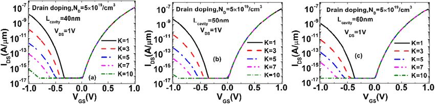
Silicon

      free detection: analytical modeling study and sensitivity analysis.    15.   Dwivedi P, Singh R (2020) Investigation the impact of the gate
      IEEE Trans Electron Devices 59(10):2809–2817                                 work-function and biases on the sensing metrics of TFET based
 4.   Sarkar D, Banerjee K (2012) Fundamental limitations of                       biosensors. Eng Res Express 2(2):025043
      conventional-FET biosensors: quantum-mechanical-tunneling to           16.   Singh D, Pandey S, Nigam K, Sharma D, Yadav DS, Kondekar P
      the rescue. Device Res Conf - Conf Dig DRC:83–84                             (2017) A charge-plasma-based dielectric-modulated Junctionless
 5.   Kanungo S, Chattopadhyay S, Gupta PS, Sinha K (2016) Study and               TFET for biosensor label-free detection. IEEE Trans on Elec Dev
      analysis of the effects of SiGe source and pocket doped channel on           64(1):271–278
      sensing performance of dielectrically modulated tunnel FET based       17.    Kim SW, Kim JH, Liu TK, Choi WY, Park B (2016)
      biosensor. IEEE Trans Electron Devices 63(6):2589–2596                        Demonstration of L-shaped tunnel field-effect transistors. IEEE
 6.   Kanungo S, Chattopadhyay S, Gupta PS, Rahaman H (2015)                        Tran Elec Dev 63(4):1774–1778
      Comparative performance analysis of the dielectrically modulated       18.   The International Technology Roadmap for Semiconductors
      full-gate and short-gate tunnel FET-based biosensors. IEEE Trans             (ITRS) (2015) [Online]. Available: http://www.itrs2.net
      Electron Devices 62(3):994–1001                                        19.   Abdi DB, Jagadesh Kumar M (2014) Controlling Ambipolar cur-
 7.   Narang R, Saxena M, Gupta M (2015) Comparative analysis of                   rent in tunneling FETs using overlapping gate-on-drain. IEEE J
      dielectric- modulated FET and TFET based biosensor. IEEE                     Electron Devices Soc 2(6):187–190
      Trans Nanotechnol 14(3):427–435                                        20.   SILVACO Inc (2016) ATLAS user’s manual,” A 2-D Device
 8.   Ghosh B, Akram MW (2013) Junction less tunnel field-effect tran-             Simulator Software Package, Santa Clara, CA, USA, [Online].
      sistor. IEEE Electron Device Lett 34(5):584–586                              Available: http://www.silvaco.com
 9.   Chandan VB, Nigam K, Sharma D (2018) Junctionless based di-
                                                                             21.   Ashita LSA, Alharbi AG, Rafat M (2018) Ambipolar leakage sup-
      electric modulated electrically doped tunnel FET based biosensor
                                                                                   pression in electron–hole bilayer TFET: investigation and analysis.
      for label-free detection. IET Circuits, Devices Syst 13(4):452–456
                                                                                   J Comput Electron 17:977–985
10.    Sarkar D, Banerjee K (2012) Proposal for tunnel-field-
                                                                             22.   Hu VPH, Wang CT (2018) Optimization of III–V heterojunction
       effecttransistor as ultra-sensitive and label-free biosensors. Appl
                                                                                   tunnel FET with non-uniform channel thickness for performance
       Phys Lett 100(14):143108
                                                                                   enhancement and ambipolar leakage suppression. Jpn J Appl Phys
11.   Im H, Huang XJ, Gu and Choi Y K 2007 A dielectric-modulated
                                                                                   57(4S):04FD18
      field-effect transistor for biosensing. Nature Nanotech 2:430–434
12.   Verma M, Tirkey S, Yadav S, Sharma D, Yadav DS (2017)                  23.   Imenabadi RM, Saremi M, Vandenberghe WG (2017) A novel
      Performance assessment of a novel vertical dielectrically modulat-           PNPN-like Z-shaped tunnel field- effect transistor with improved
      ed TFET-based biosensor. IEEE Tran on Elec Dev 64(9):3841–                   Ambipolar behavior and RF performance. IEEE Tran on Elec Dev
      3848                                                                         64(11):4752–4758
13.   Kumar S, Singh Y, Singh B, Tiwari PK (2020) Simulation study of        24.   Abdi DB, Kumar MJ (2015) Dielectric modulated overlapping
      dielectric modulated dual channel trench gate TFET-based biosen-             gate-on-drain tunnel-FET as a label-free biosensor. Superlattice
      sor. IEEE Sensors J 20(21):12565–12573                                       Microst 86:198–202
14.   Venkatesh P, Nigam K, Pandey S, Sharma D, Kondekar PN (2017)
      A dielectrically modulated electrically doped tunnel FET for appli-    Publisher’s Note Springer Nature remains neutral with regard to jurisdic-
      cation of label free biosensor. Superlattice Microst 109:470–479       tional claims in published maps and institutional affiliations.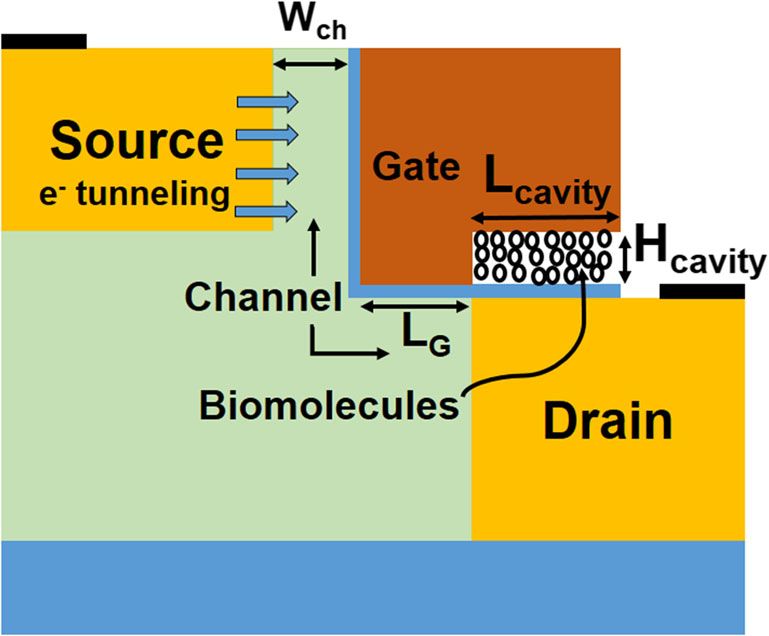
You can also read