HIGH-PERFORMANCE, HIGHLY BENDABLE MOS2 TRANSISTORS WITH HIGH K DIELECTRICS FOR FLEXIBLE LOW-POWER SYSTEMS - THE UNIVERSITY OF TEXAS AT AUSTIN
←
→
Page content transcription
If your browser does not render page correctly, please read the page content below
ARTICLE
High-Performance, Highly Bendable
MoS2 Transistors with High‑K
Dielectrics for Flexible Low-Power
Systems
Hsiao-Yu Chang,† Shixuan Yang,‡ Jongho Lee,† Li Tao,† Wan-Sik Hwang,§ Debdeep Jena,§ Nanshu Lu,‡ and
Deji Akinwande†,*
†
 Microelectronics Research Center and the Department of Electrical and Computer Engineering, The University of Texas at Austin, Austin, Texas 78758, United States,
‡
 Department of Aerospace Engineering and Engineering Mechanics, The University of Texas at Austin, Austin, Texas 78712, United States, and §Department of
Electrical Engineering, University of Notre Dame, Notre Dame, Indiana 46556, United States

    ABSTRACT While there has been increasing studies of MoS2 and other two-dimensional (2D)
    semiconducting dichalcogenides on hard conventional substrates, experimental or analytical
    studies on flexible substrates has been very limited so far, even though these 2D crystals are
    understood to have greater prospects for flexible smart systems. In this article, we report detailed
    studies of MoS2 transistors on industrial plastic sheets. Transistor characteristics afford more than
    100x improvement in the ON/OFF current ratio and 4x enhancement in mobility compared to
    previous flexible MoS2 devices. Mechanical studies reveal robust electronic properties down to a bending radius of 1 mm which is comparable to previous
    reports for flexible graphene transistors. Experimental investigation identifies that crack formation in the dielectric is the responsible failure mechanism
    demonstrating that the mechanical properties of the dielectric layer is critical for realizing flexible electronics that can accommodate high strain. Our
    uniaxial tensile tests have revealed that atomic-layer-deposited HfO2 and Al2O3 films have very similar crack onset strain. However, crack propagation is
    slower in HfO2 dielectric compared to Al2O3 dielectric, suggesting a subcritical fracture mechanism in the thin oxide films. Rigorous mechanics modeling
    provides guidance for achieving flexible MoS2 transistors that are reliable at sub-mm bending radius.

KEYWORDS: MoS2 . flexible transistor . polyimide . graphene . field-effect transistor . transition metal dichalcogenides . mobility .
bending radius . crack formation . critical strain

F
       uture ubiquitous smart electronic sys-                   outstanding radio frequency properties;510
       tems are envisioned to afford arbitrary                   however, its lack of a bandgap is a major
       form factors, robust elasticity, high                    drawback since low-power switching or digital
speed charge transport, and low-power con-                      transistors cannot be realized.11 This drawback
sumption, a combined set of attributes that                     has consequently motivated the search for
transcend existing Si-based electronics.13 Ide-                other layered atomic sheets with substantial
ally, these smart systems will be integrated                    bandgaps such as the semiconducting transi-
and realized seamlessly on environmentally                      tion metal dichalcogenides (TMDs).12,13
friendly flexible or plastic substrates. A major                    Molybdenum disulfide (MoS2) is a proto-
contemporary challenge concerns the choice                      typical TMD that has been attracting rapidly
of the semiconducting material suitable for                     growing interest owing to its large semi-
high-performance field-effect transistors (FETs)                  conducting bandgap (∼1.8 eV for mono-
on a flexible substrate.1,2,4 In the past decade,                layer and ∼1.3 eV for bulk films), which is
organic and amorphous silicon have been                         ideal for low-power electronics on hard                         * Address correspondence to
widely explored but their carrier mobilities                                                                                    deji@ece.utexas.edu.
                                                                and soft substrates.12,1418 In addition, its re-
(typically e1 cm2/V 3 s) are too low for high-                  ported high carrier mobility (up to 200 cm2/V 3 s               Received for review March 22, 2013
speed transistors operating at nanosecond                       at room temperature),17 high strength,19                        and accepted May 13, 2013.
cycles.1,4 More recently, graphene has at-                      and large surface to volume ratio make it a
                                                                                                                                Published online May 13, 2013
tracted substantial interest for high-perfor-                   compelling semiconducting nanomaterial for                      10.1021/nn401429w
mance flexible electronics owing to its high                     high speed flexible transistors and sensors. Pu
carrier mobility (>10 000 cm2/V 3 s) and                        et al. reported a flexible MoS2 FET with ion-gel                 C 2013 American Chemical Society

CHANG ET AL.                                                                                    VOL. 7     ’   NO. 6     ’   5446–5452        ’   2013                          5446
                                                                                                                                                           www.acsnano.org
ARTICLE
Figure 1. (a) AFM analysis shows the thickness of a MoS2 flake which is around 15 nm. The height profile of MoS2 flake is
scanned along the dotted line. (b) From the Raman spectrum of the MoS2 flake, the peak spacing between the E12g and A1g
vibration mode is 25 cm1 confirming that the MoS2 flake is a multilayer film.28 (c) The schematic depiction of the flexible
bottom gate device structure. (d) The optical microscope picture for the MoS2 device after the S/D patterned by e-beam
lithography. The channel length is 1 μm and the MoS2 flake with thickness of around 10 nm shows dark blue color in the
optical image. (e) The photograph of the flexible sample made on industrial polyimide sheet with cured liquid PI on the
surface (total thickness is ∼102 μm).

gate dielectric that showed high flexibility.16 However,       tensile strain. These results indicate that MoS2 is likely
the low cutoff frequency (∼107), highest mo-        tion and the optical microscope image of the MoS2
bilities (∼30 cm2/V-s), highest gate control (subthreshold    device made on polyimide. Figure 1e displays the
slope ∼82 mV/decade), and intrinsic gain above 100 on         photograph of the fabricated flexible sample.
flexible substrates at ambient conditions. Furthermore, a         Electrical characteristics of the flexible MoS2 FETs were
study of the device mechanical flexibility reveals robust      then evaluated under ambient conditions. Representative
characteristics down to a bending radius of 1 mm.             transfer (IDVG) characteristics are shown in Figure 2a,b.
Comparative studies of the two high-k dielectrics (Al2O3      The extracted low-field mobility of the fastest device is
and HfO2) used in this research determine that crack          30 cm2/(V 3 s) (Figure 2c) using the Y-function method
                                                                                      √
formation in the dielectric is the failure mechanism. The     which is defined as ID/ gm (ID is the drain current, gm is the
crack propagation velocity is substantially reduced in        transconductance) and is especially suitable for studying
HfO2 owing to its lower Young's modulus,2224 which           device physics because it excludes the contact resistance
in addition to its higher permittivity, suggests it is a      effect on the mobility.29,30 The details of the mobility
superior gate dielectric in terms of both electrical and      extraction are provided in the Supporting Information
mechanical properties particularly under momentary            (Figure S2 and S3 in the Supporting Information). Our

CHANG ET AL.                                                           VOL. 7   ’   NO. 6   ’   5446–5452   ’   2013                        5447
                                                                                                                       www.acsnano.org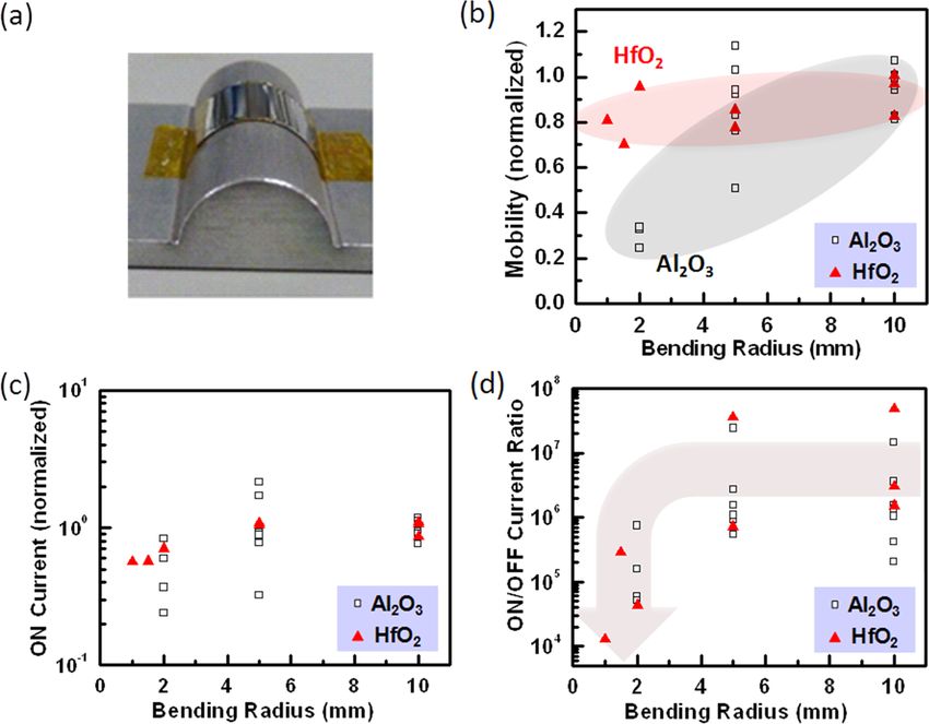
ARTICLE
Figure 2. A representative MoS2 FET (W/L = 3/1 μm) made with Al2O3 as gate dielectric on flexible PI. (a) IDVG characteristics
in log scale. The ON/OFF current ratio is more than 7 orders of magnitude, and √the subthreshold slope (SS) is ∼82 mV/decade.
(b) IDVG characteristics in linear scale. (c) The experimental Y-function (=ID/ gm) profile showing the characteristic linear
profile for extracting the low-field mobility. The extracted low-field mobility is 30 cm2/(V 3 s). (d) IDVD characteristics indicates
negligible Schottky barrier in the linear region, and current saturation at high fields.

studies of the mobilitythickness dependence reveals                order to ensure no detrimental impact to device flex-
an inverse relation (see Figure S4 in the Supporting                ibility and elasticity as we will elucidate subsequently.
Information), in agreement with a prior study over a                This will involve investigation of the parameter space of
similar thickness range.17 The ON/OFF switching ratio               the passivation material including thickness, stiffness,
is more than 107, and the subthreshold slope is ∼82                 permittivity and adhesion to the TMD to prevent dela-
mV/decade. Output (IDVD) characteristics shows neg-                mination or early cracking under deformation.
ligible Schottky barrier in the linear region, and current             Tensile strain is applied to the devices by convexly
saturation at high fields as shown in Figure 2d. In                  bending the flexible substrate using a home-built
addition, the device intrinsic gain (gm/gds) exceeded               mechanical bending fixture (Figure 3a). Electrical mea-
100, an important metric for small-signal amplification              surements were then undertaken in order to examine
(see Figure S5 in the Supporting Information). These                the stability of several device parameters that had
device characteristics represent the state-of-the-art for           been subjected to the strain condition. The device
MoS2 FETs on flexible substrates, with 4 higher                     parameters include mobility, ON current, and ON/OFF
mobility and >100 greater ON/OFF ratio compared                    switching ratio. A study of the mechanical flexibility of
to a previously reported MoS2 device.18 These results               ten devices was conducted in order to arrive at con-
are comparable with unpassivated MoS2 FETs realized                 clusions. Owing to the random orientation of MoS2
on Si substrates,14,31 indicating that its unique electri-          prepared by mechanical exfoliation, the direction of
cal properties can be accessed on hard and soft sub-                the tensile strain cannot be precisely controlled. Or-
strates alike which is a welcome benefit for flexible                 ientation measurements of the devices indicate that
electronics. Further improvement of the device perfor-              they are aligned or typically within 35° of the channel
mance can be achieved by mobility enhancement                       length direction (the current conducting direction).
through passivation with a high-k dielectric to enhance             The devices were held for 10 s at each bending radius,
the local screening effect and suppress Coulomb scat-                and then released for the measurement. The precise
tering as previously reported,14,3133 and reducing the             direction of the applied strain is not critical in this
contact resistance by using low work function metals,               study, because the devices fail due to mechanical
such as Scandium, to minimize the Schottky barrier at               fatigue of the dielectric as evidenced by crack forma-
the contact.17 However, for flexible MoS2, the device                tion which we will discuss shortly afterward. For our
passivation entails further research beyond what has                work and purpose, all our devices were mechanically
been achieved on hard substrates, requiring not just                bent until device failure was observed which allowed us
the investigation of dielectric films with high-permittiv-           to complete our mechanical modeling studies. Future
ity but also consideration of its mechanical properties in          studies will aim to evaluate the electrical performance

CHANG ET AL.                                                                 VOL. 7    ’   NO. 6   ’   5446–5452    ’   2013                        5448
                                                                                                                               www.acsnano.org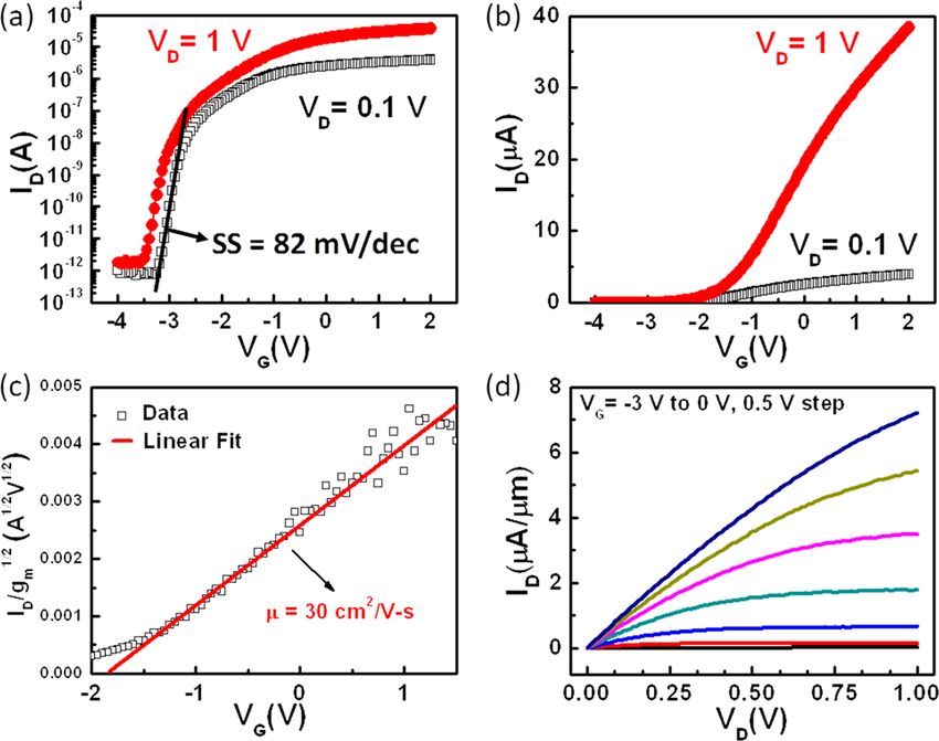
ARTICLE
Figure 3. A study of the mechanical flexibility of MoS2 FETs with Al2O3 and HfO2 gate dielectrics. (a) The photograph of the
flexible MoS2 sample at a bending radius of 5 mm on the experimental bending fixture. (b and c) The dependence of the
normalized low-field mobility (VD = 0.1 V) and ON current (VD = 1 V) on the bending radius, respectively. Mechanically robust
devices provide functional electrical characteristics down to a bending radius of 1 mm for HfO2 dielectric and 2 mm for Al2O3
dielectric. (d) The ON/OFF current ratio (VD = 1 V) versus bending radius is greater than 104 down to 1 mm bending radius for
HfO2 dielectric. Substantial degradation occurs below 1 mm bending radius owing to the onset of gate dielectric failure.

and reliability of the device as a function of the number        device sample as illustrated in Figure 4a. Without the
of mechanical bending cycles.                                    Kapton substrate, the thinner 26 um PI affords a greater
   Figure 3bd shows the dependence of the normal-               range of tensile strain to be studied, and maintained
ized mobility, normalized ON current, and ON/OFF                 the same surface property as the device structure. We
current ratio on the bending radius respectively. De-            did not perform our own measurements of the
vice characteristics are robust down to a bending                Young's modulus of each dielectric material but
radius of 1 mm for HfO2 dielectric and 2 mm for Al2O3,           materials fabricated in similar conditions are measured
which we attribute to the high deformability of MoS2,19          to have EHFO2 = 73.4 GPa, and EAl2O3 = 163.3 GPa,
and the relatively low strain placed on the dielectric           respectively.22 Stretch tests were subsequently done
thin films. For instance, MoS2 devices on HfO2 retain             using a home-built mechanical test fixture in situ under
functional properties with less than 30% mobility                optical microscope (Figure 4b). The stretch tests re-
degradation and 104 ON/OFF ratio after deformation               vealed formation of channel cracks aligned perpendi-
of 1 mm bending radius. At or below 2 mm bending                 cular to the stretch direction in the dielectric materials
radius, MoS2 devices with Al2O3 dielectric show sig-             as shown in Figure 4c. Fracture in dielectrics results in
nificant degradation owing to structural damage to the            increased scattering sites which degrades electron
dielectric. Similar significant failure was observed for          mobility and drive current. Moreover, the growing
devices with HfO2 dielectric below 1 mm bending                  density of dielectric cracks lead to increased gate
radius, while between 2 mm and 1 mm bending radius,              leakage and subsequent device failure. A quantitative
a gradual or soft degradation is observed. The Raman             count of the crack density as a function of the applied
spectrum of the MoS2 remains unchanged and the                   tensile strain can be seen in Figure 4d. The critical strain
AFM analysis shows that MoS2 with various thickness in           and saturation crack density are extracted using an
the range of 7.920.1 nm remains intact after the                empirical model that is applicable to this work.34 The
bending test, confirming that device failure is caused            result suggests a slightly higher critical strain for HfO2
by dielectric failure, but not by damage to MoS2 (see            (1.72%) compared to Al2O3 (1.69%). We found the crack
Figures S6S9 in the Supporting Information).                    density of HfO2 saturates at slightly higher values
   To unambiguously identify the mechanism respon-               (∼10%) compared to that of Al2O3, which is consistent
sible for device failure after severe bending, the gate          with the expectations that films with lower strength
dielectric structural integrity was investigated under           (σmax = Eεcr, where εcrAl2O3 ≈ εcrHfO2 but EAl2O3 > EHfO2)
varying tensile strains. For this purpose, HfO2 and Al2O3        exhibit lower saturation crack spacing.35 We note that
films are deposited on 26-μm-thick rectangular PI (PI-            device failure is not determined by saturation crack
2574) strips, with a sample cross-section similar to the         density but by the onset of crack formation and

CHANG ET AL.                                                              VOL. 7   ’   NO. 6   ’   5446–5452   ’   2013                        5449
                                                                                                                          www.acsnano.org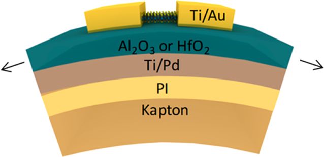
ARTICLE
Figure 4. (a) Test structure for the stretching experiments to elucidate the mechanical reliability of selected gate dielectrics
on flexible PI. (PI 26 μm/Ti 2 nm/Pd 50 nm/Al2O3 or HfO2 25 nm) (b) Photograph of the stretcher test fixture. The stretching
direction was along the x-direction. (c) Optical microscope image of the sample of HfO2 at strain ∼2.5%. The parallel cracks
aligned to the y-direction are due to tensile stress. (d) The dependence of the crack density on tensile strain for Al2O3 and
HfO2. The stretch test shows that the critical crack onset strain is around 1.69% and 1.72%, and the crack density saturates at
145 and 164 mm1 for Al2O3 and HfO2, respectively.

the velocity of crack propagation which we elucidate              from the initial status to the final status of each layer,36
subsequently.                                                     as illustrated in Figure S11. The detailed calculations
   Time-dependent observation of the crack formation              can be found in the Supporting Information. Figure S12
and propagation reveal that the crack propagation is              is used to derive the bending strain, or εb. Suppose the
substantially slower in HfO2 compared to Al2O3 (two               as-fabricated multilayer sample has an intrinsic radius
video recordings are provided as supplementary med-               of curvature R1 at the neutral axis and it is then
ia files). The measured average crack propagation                  mechanically bent to R2, if y is the distance from the
velocity is 4.9 and 28.4 μm/s for HfO2 and Al2O3,                 dielectric layer to the neutral axis, the strain in the
respectively, which is quantitatively consistent with             oxide layer due to mechanical bending is derived in the
the exponential relation between crack growth velo-               Supporting Information. Total strain (εtot) in the di-
city V and the energy release rate (G ∼ Eε2, where                electrics is then the superposition of the thermal strain
εcrAl2O3 ≈ εcrHfO2 but EAl2O3 > EHfO3) for subcritical fracture   and the bending strain, i.e., εtot = εt þ εb, which
in thin oxide films.23,24 This measurement suggests                corresponds to the total stress in the dielectrics. Ther-
that HfO2 dielectric will be more reliable under mo-              mal strain, bending strain, and total strain are shown
mentary deformation while the reliability under stea-             graphically as functions of substrate thickness (ts) and
dy-state conditions is expected to be similar.                    substrate modulus (Es) at a given bending radius in
   To reveal the controlling parameters on device                 Figure S13. It is visually revealed in the plot that
bendability, we perform detailed mechanics analysis               although the εtot curve mainly follows the shape of
in dielectric thin films accounting for both residual              the εb curve, the contribution from εt is nontrivial, and
strain due to thermal process during sample fabrica-              therefore cannot be omitted.
tion and mechanical strain induced by the bending                    To determine the bendability of the device, i.e., the
test. Sample fabrication involved several steps of                minimum bending radius measured from the bottom
thermal process. For example, the liquid polyimide (PI-           of the device before the dielectric layer starts to crack
2574) is cured at 300 °C on the Kapton substrate and              (rmin), we take the criterion of εtot = εcr for the dielectric
the dielectric was deposited at 200 °C by ALD. Mis-               layer, where εcr is the critical crack onset strain as is
match of the coefficients of thermal expansion (CTE) in             measured in Figure 4d. Solving this equation yields the
the multilayers will induce residual stresses and an              rmin as a function of the thickness and Young's modulus
intrinsic curvature to the elastic multilayer stack before        of the substrate (ts and Es), as well as the thickness and
the bending test. The strain in the dielectric layer              Young's modulus of the dielectric layer (td and Ed). The
corresponding to the residual stress due to thermal               result shows very weak dependence of rmin on td or Ed,
process is named thermal strain, or εt. It can be                 but rather quite sensitive to ts and Es. Figure 5a shows
calculated by just considering the temperature change             the minimum bending radius, rmin, as a function of the

CHANG ET AL.                                                                VOL. 7   ’   NO. 6   ’   5446–5452   ’   2013                        5450
                                                                                                                            www.acsnano.org
ARTICLE
Figure 5. (a) The predicted minimum bending radius (rmin) as a function of the substrate thickness with substrate modulus
fixed at Es = 2.5 GPa (Kapton). (b) The predicted minimum bending radius as a function of the substrate modulus with
substrate thickness fixed at ts = 76 μm. Curves in (a) and (b) are representative of both HfO2 and Al2O3 films. Decreasing the
substrate thickness or modulus can enhance the bendability of the flexible device. The dashed lines in the figures represent
the conditions closest to the current experimental samples.
substrate thickness ts for a given substrate material, breakdown or complete device failure are observed at a
Kapton (Es = 2.5 GPa). Since there is little effect from bending radius of 2 mm for both HfO2 and Al2O3 di-
dielectric modulus and thickness, this curve is repre- electrics respectively (Figure 3).
sentative of both Al2O3 and HfO2 thin films used in this
paper under steady-state or long-term tensile strain. CONCLUSIONS
The plot reveals that decreasing the substrate thick- In summary, we report the first comprehensive
ness is an effective way to enhance the bendability of studies of MoS2 FETs using conventional solid-state
the flexible transistor. This is because decreased sub- high-k dielectrics on flexible substrates. Our studies
strate thickness will shift the neutral axis closer to the yield the highest MoS2 device properties on flexible
dielectric layer. The linearity of the curve in Figure 5a substrates to date, with ON/OFF ratio greater than 107,
arises from the coincidence that we are using Kapton subthreshold slope of ∼82 mV/decade, and low-field
as the substrate which has the same modulus as the mobility of 30 cm2/(V 3 s). Furthermore, experimental
liquid polyimide. If we fix the thickness of the substrate investigation of the mechanical flexibility reveals that
to be 76 μm and vary the substrate modulus, the device characteristics are functional down to a bend-
minimum bending radius is shown in Figure 5b. It is ing radius of 1 mm for HfO2 gate dielectric. Compara-
clear that the softer substrate will offer better bend- tive studies of the two high-k dielectrics (Al2O3 and
ability. It is because decreased substrate modulus will HfO2) used in this research determine that HfO2 affords
also shift the neutral axis closer to the dielectric layer. a slower crack propagation which, in addition to its
As a result, the limiting bending radius of our sample higher permittivity, makes it a more attractive gate
could be as small as 0.45 mm if ultrathin or ultrasoft dielectric especially for momentary device deforma-
substrates are employed. Dashed lines in both figures tion. These results indicate that MoS2 is likely the most
highlight the conditions closest to the current experi- suitable semiconducting material for low-power, high
mental samples. The model predicts a minimum allow- speed devices for flexible electronics, and smart sys-
able bending radius of 2.55 mm, which is consistent tems owing to its unique combination of large band-
with the experimental observation that gradual electrical gap, high mobility, and high strength.
MATERIALS AND METHODS the Raman spectroscopy of MoS2 samples. A Veeco tapping-
mode atomic force microscope was used for thickness, mor-
Material and Device Preparation. We used commercially avail-
phology and surface analysis.
able polyimide (Kapton) with a thickness of 76 μm as the flexible
substrate, and spin-coated an additional liquid polyimide film Conflict of Interest: The authors declare no competing
(PI-2574 from HD Micro Systems) on the surface with a thickness financial interest.
of 26 μm to reduce the surface roughness. The liquid polyimide
was cured at 300 °C for 1 h. Ti/Pd (2/50 nm) deposited by Acknowledgment. This work was supported in part by the
electron beam evaporation was used as the bottom gate Office of Naval Research and the NSF-NASCENT Engineering
electrode, and Al2O3 or HfO2 (25 nm) deposited at 200 °C by Research Center. The experimental work has been carried out at
atomic layer deposition (ALD) method as the gate dielectric. the Microelectronic Research Center, a facility supported by the
National Nanotechnology Infrastructure Network (NNIN). H.-Y.
MoS2 devices were prepared by mechanical exfoliation from
Chang acknowledges financial support from the Study Abroad
commercial crystals (SPI supplies) onto the flexible substrate for
Scholarship provided by Taiwanese government.
this study. Source/drain contacts were defined by electron
beam lithography, and Ti/Au (2/50 nm) were deposited by Supporting Information Available: Additional data and anal-
electron beam evaporation followed by the lift off process. ysis, including device characteristics and the hysteresis of the
Material Characterization. Renishaw In-Via Raman Microscope MoS2 devices, the method of extracting low-field electron mobi-
with HeCd blue laser (442 nm wavelength) was employed for lity, Raman spectra before and after the bending test, and the
CHANG ET AL. VOL. 7 ’ NO. 6 ’ 5446–5452 ’ 2013 5451
www.acsnano.orgARTICLE
tensile strain modeling. Two videos about the propagation of 21. Lee, J.; Kaake, L. G.; Cho, J. H.; Zhu, X. Y.; Lodge, T. P.; Frisbie,
cracks in both Al2O3 and HfO2 are also provided. This material is C. D. Ion Gel-Gated Polymer Thin-Film Transistors: Operat-
available free of charge via the Internet at http://pubs.acs.org. ing Mechanism and Characterization of Gate Dielectric
Capacitance, Switching Speed, and Stability. J. Phys. Chem.
C 2009, 113, 8972–8981.
REFERENCES AND NOTES 22. Ilic, B.; Krylov, S.; Craighead, H. Young's Modulus and
1. Nathan, A.; Ahnood, A.; Cole, M. T.; Sungsik, L.; Suzuki, Y.; Density Measurements of Thin Atomic Layer Deposited
Hiralal, P.; Bonaccorso, F.; Hasan, T.; Garcia-Gancedo, L.; Films Using Resonant Nanomechanics. J. App. Phys. 2010,
Dyadyusha, A.; et al. Flexible Electronics: The Next Ubiqui- 108, No. 044317.
tous Platform. Proc. IEEE 2012, 100, 1486–1517. 23. He, J.; Xu, G.; Suo, Z. Experimental Determination of Crack
Driving Forces in Integrated Structures. AIP Conf. Proc.
2. Reuss, R. H.; Chalamala, B. R.; Moussessian, A.; Kane, M. G.;
2004, 3.
Kumar, A.; Zhang, D. C.; Rogers, J. A.; Hatalis, M.; Temple, D.;
24. Tsui, T. Y.; McKerrow, A. J.; Vlassak, J. J. Constraint Effects on
Moddel, G.; et al. Macroelectronics: Perspectives on Tech-
Thin Film Channel Cracking Behavior. J. Mater. Res. 2005,
nology and Applications. Proc. IEEE 2005, 93, 1239–1256.
20, 2266–2273.
3. Lee, J.; Tao, L.; Parrish, K. N.; Hao, Y.; Ruoff, R. S.; Akinwande, 25. Liu, K. K.; Zhang, W.; Lee, Y. H.; Lin, Y. C.; Chang, M. T.; Su,
D. Multi-Finger Flexible Graphene Field Effect Transistors C. Y.; Chang, C. S.; Li, H.; Shi, Y.; Zhang, H.; et al. Growth of
with High Bendability. Appl. Phys. Lett. 2012, 101, 252109– Large-Area and Highly Crystalline MoS2 Thin Layers on
2521094. Insulating Substrates. Nano Lett. 2012, 12, 1538–1544.
4. Chason, M.; Brazis, P. W.; Zhang, J.; Kalyanasundaram, K.; 26. Lee, Y. H.; Zhang, X. Q.; Zhang, W.; Chang, M. T.; Lin, C. T.;
Gamota, D. R. Printed Organic Semiconducting Devices. Chang, K. D.; Yu, Y. C.; Wang, J. T.; Chang, C. S.; Li, L. J.; et al.
Proc. IEEE 2005, 93, 1348–1356. Synthesis of Large-Area MoS2 Atomic Layers with Chemi-
5. Geim, A. K.; Novoselov, K. S. The Rise of Graphene. Nat. cal Vapor Deposition. Adv. Mater. 2012, 24, 2320–2325.
Mater. 2007, 6, 183–191. 27. Zhan, Y.; Liu, Z.; Najmaei, S.; Ajayan, P. M.; Lou, J. Large-Area
6. Petrone, N.; Dean, C. R.; Meric, I.; van der Zande, A. M.; Vapor-Phase Growth and Characterization of MoS2 Atom-
Huang, P. Y.; Wang, L.; Muller, D.; Shepard, K. L.; Hone, J. ic Layers on a SiO2 Substrate. Small 2012, 8, 966–971.
Chemical Vapor Deposition-Derived Graphene with Elec- 28. Lee, C.; Yan, H.; Brus, L. E.; Heinz, T. F.; Hone, J.; Ryu, S.
trical Performance of Exfoliated Graphene. Nano Lett. Anomalous Lattice Vibrations of Single-and Few-Layer
2012, 12, 2751–2756. MoS2. ACS Nano 2010, 4, 2695–2700.
7. Petrone, N.; Meric, I.; Hone, J.; Shepard, K. L. Graphene 29. Ghibaudo, G. New Method for the Extraction of MOSFET
Field-Effect Transistors with Gigahertz-Frequency Power Parameters. Electron. Lett. 1988, 24, 543–545.
Gain on Flexible Substrates. Nano Lett. 2012, 13, 121–125. 30. Fleury, D.; Cros, A.; Brut, H.; Ghibaudo, G. In New Y-Func-
8. Lin, Y. M.; Dimitrakopoulos, C.; Jenkins, K. A.; Farmer, D. B.; tion-Based Methodology for Accurate Extraction of Electri-
Chiu, H. Y.; Grill, A.; Avouris, P. 100-GHz Transistors from cal Parameters on Nano-Scaled MOSFETs, IEEE
Wafer-Scale Epitaxial Graphene. Science 2010, 327, 662. International Conference on Microelectronic Test Struc-
9. Ramón, M. E.; Parrish, K. N.; Chowdhury, S. F.; Magnuson, tures, ICMTS 2008; March 2427, 2008; IEEE: New York,
C. W.; Movva, H. C. P.; Ruoff, R. S.; Banerjee, S. K.; Akin- 2008; pp 160165.
wande, D. Three-Gigahertz Graphene Frequency Doubler 31. Wang, H.; Yu, L.; Lee, Y.-H.; Shi, Y.; Hsu, A.; Chin, M. L.; Li, L.-J.;
on Quartz Operating Beyond the Transit Frequency. IEEE Dubey, M.; Kong, J.; Palacios, T. Integrated Circuits Based
Trans. Nanotechnol. 2012, 11, 877–883. on Bilayer MoS2 Transistors. Nano Lett. 2012, 12, 4674–
10. Lee, J.; Parrish, K. N.; Chowdhury, S. F.; Ha, T.-J.; Hao, Y.; Tao, L.; 4680.
Dodabalapur, A.; Ruoff, R. S.; Akinwande, D. State-of- 32. Jena, D.; Konar, A. Enhancement of Carrier Mobility in
the-art Graphene Transistors on Hexagonal Boron Nitride, Semiconductor Nanostructures by Dielectric Engineering.
High-k, and Polymeric Films for GHz Flexible Analog Nano- Phys. Rev. Lett. 2007, 98, 136805.
electronics. In IEDM Technical Digest; IEEE: New York, 2012. 33. Liu, H.; Ye, P. D. MoS2 Dual-Gate MOSFET With Atomic-
11. Schwierz, F. Graphene Transistors. Nat. Nanotechnol. Layer-Deposited as Top-Gate Dielectric. IEEE Electron De-
2010, 5, 487–496. vice Lett. 2012, 33, 546–548.
12. Neto, A. H. C.; Novoselov, K. New Directions in Science and 34. Jen, S. H.; Bertrand, J. A.; George, S. M. Critical Tensile and
Technology: Two-Dimensional Crystals. Rep. Prog. Phys. 2011, Compressive Strains for Cracking of Al2O3 Films Grown by
74, 082501. Atomic Layer Deposition. J. App. Phys. 2011, 109, No.
13. Xu, M.; Liang, T.; Shi, M.; Chen, H. Graphene-Like Two- 084305.
Dimensional Materials. Chem. Rev. 2013, 113, 3766–3798. 35. Leterrier, Y.; Wyser, Y.; Månson, J.; Hilborn, J. A Method to
14. Radisavljevic, B.; Radenovic, A.; Brivio, J.; Giacometti, V.; Kis, Measure the Adhesion of Thin Glass Coatings on Polymer
A. Single-Layer MoS2 Transistors. Nat. Nanotechnol. 2011, Films. J. Adhes. 1994, 44, 213–227.
6, 147–150. 36. Hsueh, C. Thermal Stresses in Elastic Multilayer Systems.
15. Kim, S.; Konar, A.; Hwang, W.-S.; Lee, J. H.; Lee, J.; Yang, J.; Thin Solid Films 2002, 418, 182–188.
Jung, C.; Kim, H.; Yoo, J.-B.; Choi, J.-Y.; et al. High-Mobility
and Low-Power Thin-Film Transistors Based on Multilayer
MoS2 Crystals. Nat. Commun. 2012, 3, 1011.
16. Pu, J.; Yomogida, Y.; Liu, K. K.; Li, L. J.; Iwasa, Y.; Takenobu, T.
Highly Flexible MoS2 Thin-Film Transistors with Ion Gel
Dielectrics. Nano Lett. 2012, 12, 4013–4017.
17. Das, S.; Chen, H. Y.; Penumatcha, A. V.; Appenzeller, J. High
Performance Multilayer MoS2 Transistors with Scandium
Contacts. Nano Lett. 2013, 13, 100–105.
18. Yoon, J.; Park, W.; Bae, G. Y.; Kim, Y.; Jang, H. S.; Hyun, Y.; Lim,
S. K.; Kahng, Y. H.; Hong, W. K.; Lee, B. H.; et al. Highly Flexible
and Transparent Multilayer MoS2 Transistors with Graphene
Electrodes. Small 2013, 10.1002/smll.201300134.
19. Bertolazzi, S.; Brivio, J.; Kis, A. Stretching and Breaking of
Ultrathin MoS2. ACS Nano 2011, 5, 9703–9709.
20. Cho, J. H.; Lee, J.; He, Y.; Kim, B. S.; Lodge, T. P.; Frisbie, C. D.
High-Capacitance Ion Gel Gate Dielectrics with Faster
Polarization Response Times for Organic Thin Film Tran-
sistors. Adv. Mater. 2008, 20, 686–690.
CHANG ET AL. VOL. 7 ’ NO. 6 ’ 5446–5452 ’ 2013 5452
www.acsnano.orgYou can also read