Hijacking Power and Bandwidth from the Mobile Phone's Audio Interface
←
→
Page content transcription
If your browser does not render page correctly, please read the page content below
Hijacking Power and Bandwidth
                           from the Mobile Phone’s Audio Interface

                                            Ye-Sheng Kuo, Thomas Schmid, Prabal Dutta
                                                    Computer Science & Engineering Divison
                                                            University of Michigan
                                                             Ann Arbor, MI 48109
                                                 {samkuo,thschmid,prabal@eecs.umich.edu

ABSTRACT
We endow the digital mobile phone with an analog interface that
can parasitically power external peripherals and transfer data to and
from them using the existing headset interface. Our design delivers
several milliwatts at 3 V to a load and offers a bidirectional com-
munications channel at a data rate of 300 bps. We demonstrate a
simple oscilloscope application using this new functionality.                                      1234
                                                                                     Figure 1: The iPhone headset plug and its pinout. iPhones use
1.     INTRODUCTION                                                                  a 3.5 mm phono jack/plug to output audio to headphones and
   The mobile phone is the most pervasive personal communica-                        receive input from a microphone. The headphone connections
tions and computing platform ever created and yet, among its var-                    are: (1) left earphone (tip), (2) right earphone (ring), (3) com-
ious analog interfaces, only one is open, standardized, and widely                   mon/ground (ring), and (4) microphone (sleeve). The measured
accessible: the headset port. In this paper, we take a closer look                   impedance between the left (or right) earphone and common is
at this ubiquitous interface and assess its utility for augmenting the               33 Ω. The measured impedance between the microphone and
mobile phone with a range of phone-powered peripherals. We show                      common is approximately 640 Ω.
that the mobile phone headset port can be used to efficiently power
external peripherals and communicate with them, enabling many
new phone-centric applications. But, why use the headset port at                         This project poses several engineering and research challenges.
all? One reason is that it is an open, simple, and ubiquitous inter-                 The output from the audio jack is a low voltage signal, often even
face with documented electrical and mechanical specifications, as                    lower than typical transistor threshold voltages. To be useful, it
Figure 1 shows. Perhaps even more important, the headset interface                   must be converted to a higher voltage using energy harvesting and
is backward- and forward-compatible with most mobile phones in                       voltage boosting circuits that can operate with input AC voltages in
use today, so the mobile phone could form the basis for many health                  the 200 mV level. Due to the limited voltage headroom, simple rec-
and communications applications in developing regions.                               tification is difficult without substantial power losses. It may also
   The motivation for such mobile phone peripherals comes from                       require maximum power point tracking. Matching the harvesting
several quarters. First, the emergence of mobile phone accessories                   circuit’s cost, complexity, and conversion efficiency with the ideal
like the Square Card Reader [1] suggest that simple peripherals that                 audio waveform also presents an iterative co-design problem. Us-
can leverage the headset port have commercial appeal. Second, re-                    ing the audio output to deliver power and data functionality requires
searchers focused on developing regions have a need for low-power                    exploring several design tradeoffs and concerns.
vital signs devices that could directly interface to a mobile phone                      In this paper, we characterize the power available from the au-
and be powered from it. Third, leading academics have argued for                     dio jack, design a circuit to harvest this power, and evaluate the
reformulating introductory computer science curriculums around                       efficiency of the conversion. We find that the headset can deliver
the mobile phone, but this paper shows how many important elec-                      approximately 16 mW per channel from the iPhone’s headset port.
trical engineering concerns like power, communications, and em-                      We present a circuit that can harvest energy from a single chan-
bedded systems can also be explored in this context. This proposal                   nel and an audio signal that when played on the phone can maxi-
seeks to enable additional devices like the Square Card Reader, pro-                 mize the output power from the harvesting circuit. We also demon-
vide a basis for new phone peripherals, and enable greater student                   strate that a pair of (coded) audio signals can be generated by the
engagement by allowing EECS students to tinker with their phones.                    phone processor and transmitted to both the energy harvesting cir-
                                                                                     cuit (power) and a microcontroller (signal) and where the signal can
                                                                                     be decoded by the microcontroller. Conversely, we show that the
                                                                                     microcontroller can also generate a coded signal that can be read
Permission to make digital or hard copies of all or part of this work for            by the mobile phone’s microphone input and decoded by the phone
personal or classroom use is granted without fee provided that copies are            to present a stream of digital data. Finally, integrating all of the var-
not made or distributed for profit or commercial advantage and that copies           ious pieces, we present a simple oscilloscope application that runs
bear this notice and the full citation on the first page. To copy otherwise, to      partly on the mobile phone and partly on an external microcon-
republish, to post on servers or to redistribute to lists, requires prior specific   troller powered using the mobile phone’s right audio channel. The
permission and/or a fee.
ISLPED’10 Design Contest Austin, TX, USA                                             two processors communicate using the left audio channel (phone to
Copyright 200X ACM X-XXXXX-XX-X/XX/XX ...$10.00.                                     microcontroller) and microphone (microcontroller to phone).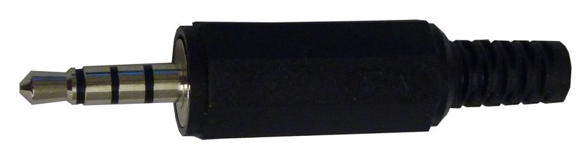
2. ENERGY HARVESTING
Our first design goal is to harvest energy from the headset jack
of a mobile phone, convert it into a more usable form, and achieve
high conversion efficiency in the process. We begin by characteriz-
ing the AC waveforms that are available, the output impedance of
the headset port, and the range of variables available for manipula-
tion. We then design and evaluate an energy harvesting circuit to
convert the available power into a more usable form.
2.1 Determining Available Power
We now explore the question of how much power can be har-
vested from iPhone’s headset port. To do so, we use the Faber
Acoustical iPhone SignalScope Pro software [2] to generate a range
of audio frequencies, from 20 Hz to 24 kHz, and output them over
the iPhone’s audio port. We find that the output power is indepen-
dent of frequency, so we use a 5 kHz AC tone in our subsequent
experiments. Table 1 shows the settings to generate the output.
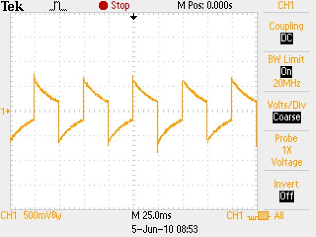
Figure 3: The audio output waveform observed when a 20 Hz
square wave is transmitted over the audio output channel. The
Parameter Value sharp transitions followed by characteristic exponential-decay
Hardware iPhone 3GS [3] curves show the output is AC-coupled, eliminating the simple
Software SignalScope Pro [2] option of driving the audio output with a constant DC voltage.
Function Signal Generator
Output Headphones
Type Tone 2.2 Design Space Exploration
Frequency 20 Hz to 24 kHz (5 kHz nom) We next explore the question of how to efficiently harvest the
Amplitude 0.00 dB energy produced from the headset output. The two engineering
Pan 0.000% challenges are to increase the signal amplitude and convert the AC
Volume Maximum signal into a DC one. Figure 2 shows that the open circuit volt-
age, Voc , is less than 500 mV and that the maximum power point
Table 1: Experiment parameters for determining the available voltage, Vmpp , occurs at 240 mV. These voltages are far below the
power from the iPhone 3GS headset port. turn on voltages of switching regulators (typically in the range of
800 mV to 900 mV). They are also below the required startup volt-
A load resistance is connected between the right audio channel age, after rectification, of ultra-low voltage step-up DC-DC con-
and common line on the headset. The load is varied from 0 Ω verters, like the Seiko S-882Z [4], which require 300 mV to start.
to 15 kΩ and the output voltage and load current are measured at Rectification losses can be significant in both high-power and
several points. A linear fit of the data yields the (essentially linear) low-voltage systems. In our case, for example, to achieve maxi-
IV curve shown in Figure 2. From these data, we generate the mum power transfer, an RMS current of 66 mA is required. When
power transfer curve, which shows that maximum power transfer rectified using even a low-Vf Schottky diode like the DFLS120L,
occurs at 240 mVrms and 66.0 mArms, for a 3.6 Ω load. a 200 mV forward voltage drop occurs (See Fig 1 in reference [5]),
meaning that 80% of the power is lost during rectification, and only
175 17.5 20% can be delivered to the load.1 Synchronous rectification is
sometimes used to reduce losses, where a FET switch is used in-
150 15 stead of a diode [10]. In low-voltage applications like ours, the
problem is generating a sufficiently high gate drive voltage to turn
Output current (mA, rms)
125 12.5 on the FET switch. Given the low voltages involved, this would
Output power (mW)
require many stages of (inefficient) voltage multiplication ladders.
100 10
We end this section on design alternatives by eliminating two
simple, but ultimately unworkable, options: harvesting DC directly
75 7.5
from the audio output and harvesting DC from the microphone bias
voltage. Figure 3 shows the waveform that is observed on the audio
50 5
output when a 20 Hz square wave signal is generated on the phone.
The characteristic exponential decay curves suggest that the output
25 2.5
is AC-coupled, and is therefore a high-pass filter that blocks DC.
0 0
This eliminates the possibility of simply generating a DC output
0 100 200 300 400 500 voltage to power the external devices. Using the microphone bias
Output voltage (mV, rms)
voltage is also difficult because we plan to use it as the data input
channel to the phone, which will be modulated externally.
Figure 2: Available power from the iPhone headset jack. These
data show that it is possible to draw 15.8 mW from an ideally- 1
matched load of 3.6 Ω, which is enough to power many low- This assumes that only a single rectifier diode is on the path, which
would of course reduce the available power by 50%. If two diodes
power electronics. To be useful, however, the power must be are on the path, as would be the case for a bridge rectifier, the losses
rectified from AC to DC, boosted to a few volts, and filtered. would be substantially higher.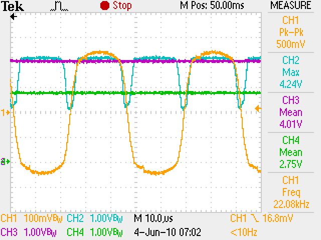
2                3                         4                          5                             6

    2.3          Harvesting Energy Efficiently                                                          2.4    Design Evaluation
       To sidestep the two basic engineering challenges – low-supply                                       To evaluate the performance of our design, we implement the
    voltage and need for rectification – we use a step-up microtrans-                                   energy harvesting
                                                                                                                 A         circuit, as shown in Figure 5. The circuit only
    former, followed by FET-based rectification, followed by (parallel)                                 requires a footprint of 1.0” x 0.35” (although the current board in-
    blocking Schottky diode(s), followed by filter capacitors, as shown                                 cludes a 0.15” unused area for manufacturing reasons) and several
    in Figure 4. One key element of the design, the microtransformer,                                   header export lines. The circuit’s small size makes it suitable for
    leverages a recently introduced device for flyback and step-up for                                  embedding inside a headset plug, like the one shown in Figure 1.
    energy harvesting applications. These new transformers are small
    (6 mm x 6 mm x 3.5 mm), have high coupling coefficients (> 0.95),
                                                                                                                B
    and are available in a range of turns ratios [6]. We use a 1:20 ratio.

                 T1
                           Q1         Q3
             1

                  4

     J1 1                                          D1
                                                                                          R1
       2    L1        L2                       A        C

                                           1 J2             C1   C2       1 J3       C3
                                                                                                        Figure 5: Energy harvesting circuit. The transformer, Schottky
                                                                                 +             D2
             2

                  3

                                           2                              2
                           Q2        Q4
                                                                                                        diode, LED,
                                                                                                                 C    and resistor are visible on the top side. The FET
                                                                                                        rectifier and filter capacitors are visible on bottom side.

                                                                                                           Figure 6 shows a trace of the circuit in operation. The iPhone
    Figure 4: The energy harvesting circuit. A 1:20 microtrans-
                                                                                                        generates a 22 kHz, 500 mV peak-to-peak square wave that is low-
    former boosts the input voltage. A FET bridge efficiently rec-
                                                                                                        pass filtered (substantially lower excitation frequencies result in
    tifies the AC signal to DC. Parallel Schottky diodes provide
                                                                                                        poor power transfer). The RMS value of the signal is 207 mV,
    low-loss blocking to prevent the output filter capacitor from
                                                                                                        meaningDthat approximately 15 mW is delivered by the phone, or
    discharging through the FET bridge. An (optional) LED with
                                                                                                        about 90% of peak power. Channel 1 (orange) shows this filtered
    current-limiting resistor provides a visual power indicator.
                                                                                                        audio output signal. Channel 2 (blue) shows a peak 4.24 V sig-
                                                                                                        nal after rectification using the FET bridge. Channel 3 (magenta)
       The stepped-voltage is passed through a FET bridge for rectifi-                                  shows the output after passing the rectified signal through (a single)
    cation. Since the stepped-up voltage is substantially higher than                                   blocking diode, which drops 230 mV at peak current, providing
    the FET threshold voltage, the FETs are in conduction and offer                                     at worst a 94.5% efficiency. Channel 4 (green) shows the voltage
    marginal loss. Another benefit to stepping-up the voltage is a re-                                  across the
                                                                                                                 E LED after the signal passes through a high-side current-
    duction in current flow through the blocking diode, and therefore                                   limiting resistor measured to be 699 Ω.
    a reduction in forward voltage drop. However, since the diode is
    an exponential device, this unfortunately does not result in a sub-
    stantial decrease in the forward voltage drop, but it does eliminate
    the voltage drop from a second diode in the rectifier. And, since
    the diode forward voltage drop is a small fraction of the rectified
    voltage, this design incurs a small inefficiency compared to direct
    rectification of the low-voltage signal.
       Matching the load and source impedances is critical to achieving
    high-efficiency power transfer from a power supply to its load. In
    this case, the impedance offered by the microtransformer’s primary
    winding should be matched to the iPhone’s audio output port’s
    impedance of 3.6 Ω. The transformer’s datasheet states that the pri-
    mary DC resistance is 200 mΩ and primary inductance is 25 µH,
    which we verified empirically. Since the transformer’s DC resis-
    tance is small compared to the power supply’s output impedance,
    we focus on the transformer’s impedance. The impedance, XL ,
    offered by an inductor is
                                 XL = jωL = j2πf L.
                                                                                                        Figure 6: Energy harvesting circuit operation. Channel 1 (or-
      Rearranging to solve for f , the desired excitation frequency, gives                              ange) shows the filtered audio excitation signal. Channel 2
                                                    XL                                                  (blue) shows the signal after rectification. Channel 3 (magenta)
                                           f=           .                                               shows the output after passing through a blocking diode which
                                                    2πL
                                                                                                        drops. Channel 4 (green) shows the voltage across the LED.
      Substituting our measured impedance and inductance values gives
                                       3.6 Ω                                                               The power supply ripple is less than ±10 mV as long as the audio
                                f=             = 22.9 kHz.                                              signal is present and the load is static. Our design currently does
                                     2π × 25µH
                                                                                                        not include voltage regulation for several reasons: (i) it may not be
       The target excitation frequency sits just at the edge of the what                                needed in some applications; (ii) it is not needed for our example
    the iPhone is capable of producing. Fortunately, however, we have                                   application; (iii) the output voltage and power supply buffering is
    complete control over the excitation frequency within the audio                                     often specific to the particular application. These results show we
    band, so we can generate a 22 kHz waveform which will achieve                                       can harvest energy from the phone’s headset port, and convert it
    near optimal power transfer to the energy harvester circuit.                                        into a more useful form, using a simple and inexpensive circuit.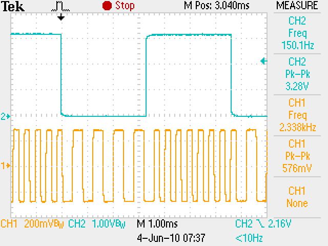
3.      DATA COMMUNICATIONS
   Our second design goal is to provide bi-directional communica-
tions between the mobile phone and a peripheral microcontroller.
The requirements for this communication channel are: (i) it must
operate in the audio frequency range, and (ii) it must be easy to
implement on a microcontroller. The second requirement is neces-
sary as we need to implement both the modulator and demodulator
functions inside of a microcontroller since most other integrated
circuits that provide a modulation and demodulation functionality
are not sufficiently low power, drawing tens of milliwatts [7].
   Given these two requirements, we use the well-established Bell
202 signaling technique. Bell 202 employs frequency shift key-
ing (FSK) using two tones. A digital zero, or “space,” is rep-
resented by a 1200 Hz tone, while a digital one, or “mark”, is
represented by a 2200 Hz tone. Unlike the Bell 202 standard,
which specifies 1200 baud communications, we chose to use a
lower data rate of 300 baud in order to facilitate an implementa-
tion on a low-power microcontroller. At the digital level, we use                             Figure 8: The data stream and its modulated transmission from
low-voltage RS-232 signaling to create a virtual universal asyn-                              the microcontroller to the phone. The top trace shows a 300 bps
chronous receiver/transmitter (UART) abstraction over the audio                               data stream, where a zero-bit is shown from 2.0 ms to 5.3 ms,
serial bit stream. Since the UART protocol adds a start and stop bit                          followed by a one-bit from 5.3 ms to 8.6 ms. The bottom trace
to every byte, the effective data rate is 30 bytes/sec.                                       shows the FSK-encoded transmission of this data, where the
   In order to efficiently implement FSK encoding and decoding on                             zero-bit is encoded as a 1200 Hz tone and the one-bit is encoded
a microcontroller, it is useful to make maximum use of the micro-                             as a 2200 Hz tone. Although the microcontroller-generated sig-
controller peripherals. W. Lutsch describes one such implemen-                                nals are square waves, they they do undergo some low-pass fil-
tation that uses several hardware features to efficiently modulate                            tering.
and demodulate FSK signals [8]. Figure 7 presents an overview of
our implementation of this software-defined radio approach. Using
these hardware accelerators allows for much lower-power opera-                                Figure 8). This signal is sent through a low-pass filter before it is
tion than would otherwise be possible.                                                        fed into the microphone port of the phone. This filtering reduces
                                                                                              the high frequency components of the square wave.
                                                                                                 The left channel headphone output is a ground-referenced AC
 From Phone      AC Coupling   Comparator    Timer Compare
                                                                   LP Filter
                                                                               To Phone Mic   signal. Unfortunately, we cannot directly process this signal in
 Left Channel     at Vcc/2      at Vcc/2       Signal Gen.
                                                                                              the microcontroller, and thus we AC couple it to a voltage divider
                                Edge Time       Tone
                                                                                              whose midpoint is set to the microcontroller’s Vcc/2. The main
                               Measurement     Encoder                                        idea behind the FSK decoder is to measure the zero-crossing time
                                                                                              of the signal, and decide on the frequency. We achieve this by com-
                                  Tone                       0/1
                                 Decoder
                                                                                              paring the signal to Vcc/2 in a comparator that is internally con-
                        0/1                                                                   nected to a timer capture unit. In software, we calculate the time
                                UART RX        UART TX                                        difference between rising and falling edges using the timer capture
  From Phone                                                                                  interrupt. The result of this decision is then output on a digital IO
 Right Channel     Power       Vcc
 Common           Harvester    GND                                                            line that is externally connected back into the receive port of the
                                                MSP430 MCU
                                                                                              UART peripheral. The UART receiver is then responsible for de-
                                                                                              coding the signal at 300 baud.
Figure 7: Data communications system architecture. The                                           Implementing the FSK encoder and decoder on the phone is eas-
phone’s headset port exports four wires: right channel, left                                  ier as we have a more powerful processor available. This allows
channel, mic, and common. The right channel provides power                                    us to use more sophisticated algorithms. We implement a non-
to the energy harvesting circuit. The left channel provides data                              coherent FSK demodulator on the phone [9]. In non-coherent FSK
output from the phone to the microcontroller. The mic pro-                                    demodulation, the incoming signal is correlated with four differ-
vides data input from the microcontroller to the phone. Both                                  ent signals, a pair of sine/cosine signals at 1200 Hz, and a pair of
the phone and the microcontroller implement FSK modulators                                    sine/cosine signals at 2200 Hz. The correlation value of the two
and demodulators.                                                                             pairs is sampled and added together. Then, the sums of the two
                                                                                              pairs are compared to each other in order to decide which frequency
   The main communication interface for an application running on                             is currently transmitted. A state machine processes the stream of
the microcontroller is the UART receiver and transmitter peripher-                            ones and zeros to detect the UART start bit, before it decodes the
als. The pins of both the receive and transmit unit of the UART are                           byte value transmitted in the FSK signal.
connected to other microcontroller peripherals for more processing.                              The FSK encoder on the phone creates a continuous-phase sig-
   On the encoder side, the UART transmitter generates the data                               nal that switches between the two tones according to the bit that is
bits at 300 baud (Channel 2, blue, on Figure 8). These bits are fed                           transmitted. Figure 9 shows the audio spectrum used by the phone.
back to the microcontroller into an interrupt line. A timer compare                           Two peaks are clearly visible at 1200 Hz and 2200 Hz, plus the
unit generates the correct frequency according to the bit coming                              22 kHz tone used to power the energy harvester. A test of the com-
from the UART transmitter. The output of the timer compare is a                               munication channel from microcontroller to phone found a bit error
square wave at either 1200 Hz or 2200Hz (Channel 1, yellow, on                                rate of 0.3 · 10−3 over a run length of 27,872 bytes.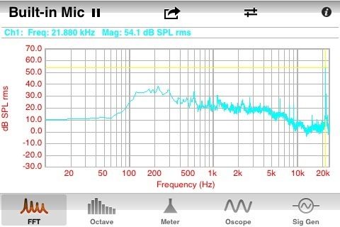
Voltage Divider Epic DevKit with Communication
with Potentiometer TI MSP430 MCU Filters
Energy Headset Simple Oscilloscope
Harvester Audio Port Application on iPhone
(a) Noise spectrum
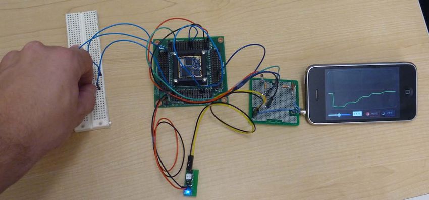
Figure 10: Prototype phone-centric oscilloscope application in
full operation. The system consists of four distinct subsystems
which are all shown working together: (i) iPhone; (ii) commu-
nication filters; (iii) energy harvester; (iv) microcontroller with
potentiometer simulating a resistive sensor. The blue LED, lo-
cated at the bottom of the energy harvester, is turned on and
clearly visible in this figure.
(b) Communications spectrum
Figure 9: Audio spectrum utilization. Figure 9(a) shows the
noise spectrum of the system (and the 22 kHz power tone). The
sound pressure level is less than 40 dB. Figure 9(b) shows the
audio spectrum with data communications and power. Two
peaks are clearly visible at 1200 Hz and 2200 Hz, as well as the
22 kHz tone used to provide power). We use the FFT function
in SignalScope Pro software on the iPhone to show the audio Figure 11: Screenshot of the iPhone Oscilloscope application.
spectrum usage of our system [2]. The slider controls the sampling rate by sending the slider value
to the microcontroller over the left audio channel. The sampled
ADC value from the microcontroller is sent to the phone over
4. APPLICATIONS the microphone channel and is visualized on the oscilloscope
Our final design goal is to show that the various pieces of the screen and displayed in a textbox next to the slider. This figure
system – energy transfer, data input, and data output – can all be illustrates integrated operation of all four system components.
combined into a single, integrated, and fully-functional application.
For that purpose, we designed a prototype handheld oscilloscope,
as shown in Figure 10. This system illustrates a canonical handheld box shows the last received measurement. The data are transmitted
instrument that uses the phone’s display for visualization, and the from the microcontroller at regular sample intervals. A slider al-
microcontroller’s ADC to measure an external signal. lows the user to change the sampling rate from about 1/10 to 30 Hz,
At the heart of this system is the application running on the the limit given the 300 bps encoding of the FSK signal. The slider
phone. It generates a 22 kHz tone on the right audio channel to setting is sent over the left channel to the microcontroller, which
power the microcontroller using the energy harvesting circuit. The decodes the signal and changes its sample rate accordingly.
left audio channel sends an FSK modulated data stream to the mi- The microcontroller draws a mere 0.7 mA at 2.8 V while running
crocontroller. The phone’s microphone input receives an FSK- the full application including FSK encoder and decoder, UART, and
modulated data stream from the microcontroller. The phone ap- ADC to sample the sensor. This is less than 2 mW, leaving signifi-
plication implements a non-coherent FSK demodulator as well as a cant power for more sophisticated sensing and signal conditioning.
continuous-phase FSK modulator. One of the motivations for harvesting energy, rather than directly
The user interface provides visual feedback to the user of the powering a peripheral with an external battery, is to reduce the form
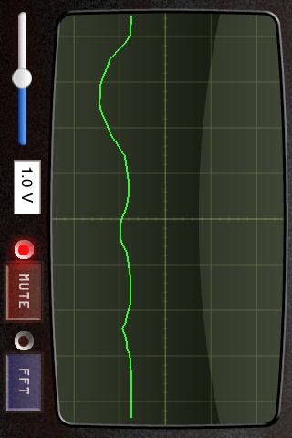
voltage measured using the microcontroller’s ADC input. Figure 11 factor of a peripheral. While the prototype is large due to the use
shows a screenshot close-up of the application running on an iPhone. of a development kit and protoboard, the active components used
The graph displays a historic view of measured data, while the text could be integrated onto a much smaller circuit board. For example,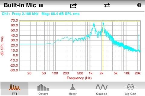
the two largest components – a transformer and a TI MSP430F1611          Acknowledgments
microcontroller – measure a mere 6 mm x 6 mm and 9 mm x 9 mm,            We would like to thank Eric Brewer for originally suggesting this
respectively. In the next version, we plan to use a newer TI MSP430      problem and the anonymous reviewers for their helpful feedback.
(
You can also read