ML4027-DCO-HLB-X Technical Reference - CFP2 DCO MCB - MSA Compliant
←
→
Page content transcription
If your browser does not render page correctly, please read the page content below

ML4027-DCO-HLB-X
  Technical Reference
 CFP2 DCO MCB – MSA Compliant

Table of Contents
1.     General Description........................................................................................................ 3
2.     ML4027-DCO-HLB-X test board – key features ................................................................ 3
3.     Ordering Information ..................................................................................................... 3
4.     Power-Up and Operation ............................................................................................... 3
     4.1      ML4027-DCO-HLB-3 .......................................................................................................... 3
     4.2      ML4027-DCO-HLB-5 .......................................................................................................... 4
5.     Operating Conditions ..................................................................................................... 4
6.     LEDs Indicators............................................................................................................... 5
7.     MDIO Interface .............................................................................................................. 5
8.     Hardware Signals ........................................................................................................... 5
     8.1      MDIO Control ................................................................................................................... 6
     8.2      HW Control ....................................................................................................................... 6
9.     FTDI Chip ....................................................................................................................... 7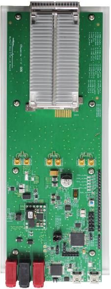
1. General Description
The ML4027-DCO-HLB-X is a CFP2-DCO Module Compliant Board. It is designed to provide an
efficient and easy method of programming and testing CFP2-DCO modules.
The ML4027-DCO-HLB-X is designed to simulate an ideal environment for CFP2-DCO module
testing, making the host board as electrically transparent as possible, and allowing a more
accurate assessment of the module performance.
2. ML4027-DCO-HLB-X test board – key features
CFP2-DCO MSA Form Factor
Supports eight TX & RX Lanes
MDIO interface
FTDI Chip accessible through USB connector
Access to Control/Alarm signals provided through pin headers
Current Sense
Voltage Sense
Temperature Sense
3. Ordering Information
Default
Part Number Description
Configuration
Single supply ML4027-DCO-HLB-3 power-up using single supply 3.3 V
Dual Supply ML4027-DCO-HLB-5 power-up using dual supply (5 V AND 3.3 V)
4. Power-Up and Operation
The powering up method depends on the default configuration, based on the part number.
The different methods are described below.
4.1 ML4027-DCO-HLB-3
The ML4027-DCO-HLB-3 part number is powered up using single supply, as described below:
1. U13 jumper should be populated
2. Connect the banana plug (U8) to 3.3 V
3. Connect the GND to the banana plug (U5)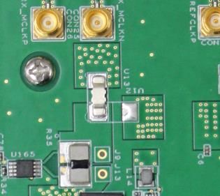
4.2 ML4027-DCO-HLB-5

The ML4027-DCO-HLB-5 part number is powered up using dual-supply, as described below:

      1.   U12 jumper must be populated
      2.   Connect banana plug (U8) to 3.3 V, AND
      3.   Connect banana plug (U14) to 5 V
      4.   Connect the GND to the banana plug (U5)

When dual supply is used, the user has the ability to control the module input voltage to one of
three voltage levels: 3.15 V, 3.3 V or 3.45 V.

The image below shows the common-pad SMD jumper, that could be populated on U12 or U13,
depending on the ordering part number.

                                                U13

                                                                U12

                                  Figure 1: SMD Jumper Population Option

After board power up, and in order to communicate to the board, connect the host to your PC
using a Type-B mini to Type-A USB cable through one of the USB connectors, depending on the
user application, where two options are available:
      1- USB_MICRO: where communication is established through the microcontroller.
      2- USB_FTDI: where communication is established through the FTDI chip.

5. Operating Conditions

Based on the used powering method, as described in the previous section, the input voltage
supply must follow the table below.

 Parameter        Symbol Condition                        Min         Typical     Max    Unit
 +5               P5V     Supply from U14 (P5V Pin)         -              +5      -
                                                                                          V
 +3.3             P3V3    Supply from U8 (P3V3 Pin)       +3.0             +3.3   +3.6
6. LEDs Indicators
The ML4027-DCO-HLB-X boards, include on-board LEDs, for quick debugging and monitoring
purposes. LEDs are summarized below:
LED D11 indicates whether a USB cable is plugged or not in the JR4 connector
(USB_MICRO).
LED D3 indicates whether a USB cable is plugged or not in the USB connector
responsible to communicate with the FTDI (USB_FTDI).
LEDs D12 and D13, are used for diagnostic purposes.
o If the green LED, D13, is on: USB is locked and device is recognized by the USB driver.
o If the red LED, D12, is on: USB not connected or USB driver not found.
o If both LEDs are off: Board not powered correctly or firmware is corrupted.
LED D7: PRG_ALRM1 signal Monitoring
LED D8: PRG_ALRM2 signal Monitoring
LED D10: PRG_ALRM3 signal Monitoring
LED D17: RX_LOS signal Monitoring
LED D18: MOD_ABS signal Monitoring
LED D16: GLB_ALRMn signal Monitoring
7. MDIO Interface
The MDIO bus can be driven from two sources: Microcontroller or FTDI chip.
The MDIO source is selected by the user by selecting jumpers placement. The placement shown
below is used when the MDIO bus is driven from the microcontroller (default placement). To
use the other option (FTDI chip), both jumpers need to be moved to the opposite position.
Figure 2: MDIO source selection
8. Hardware Signals
Hardware alarm pins, hardware control pins and MDIO pins can be accessed from the software
via USB or through on-board pin headers. The dip switch U153 (HW_CNTRL) allows switching
signaling pins control between software and hardware. And the dip switch U153 (S_MDIO) allows
to operate the board via external MDIO.The image below shows the default state of the switch, where in this case the signals are
controlled through software. To access these signals via pin headers, the switches should be
moved to the opposite side (switch to GND).
Figure 3: Dip Switch U153
8.1 MDIO Control
When the S_MDIO switch is moved to ground, the user could apply external MDIO through pin
headers as shown below.
The user could access the MDIO bus for both MDIO 3.3 V (U155 pin header) and MDIO 1.2 V
(TP4 and TP6 pins).
Figure 4: MDIO Pins
8.2 HW Control
When the HW_CTRL switch is moved to ground, the user could control the CFP2 control signals
from an external source. All the hardware control and monitor signals could be accessed
through pin headers shown below.
Figure 5: Control and Alarms SignalsAll hardware control signals can be driven directly to ground using jumpers, as shown below
(see Figure 4):
J3: PRG_CTRL3
J4: PRG_CTRL2
J5: PRG_CTRL1
J6: TX_DIS
J7: MOD_LOPWR
J19: MOD_RSTn. This is an independent pin. MOD_RSTn is connected to a switch for
easy access from the user.
Figure 6: HW Control Signals Jumpers
9. FTDI Chip
The communication with the FTDI chip is done through the USB connector JR5 (USB_FTDI). The
USB cable must be inserted in order to activate the FTDI Chip.
The FTDI has two output communications buses:
1- MDIO bus: in order to use the FTDI MDIO instead of the microcontroller MDIO bus, the
jumpers placement should be changed as described in section 7.
2- UART bus: the UART_TX and UART_RX signals are connected to J10 pin header.
Figure 7: FTDI blockAppendix
Below is a summary of board deviations:
In case of using dual supply it is expected to control the module input voltage to one of three
options: 3.15 V, 3.3 V, and 3.45 V.
o The initial state of the board is that the three options are as follow: 3.19 V, 3.3 V and
3.41 V
The currently sent boards have the correct voltage levels (starting serial number 20)
o The voltage levels are: 3.15 V, 3.3 V and 3.45 V.Revision History
Revision number Date Description
0.1 12/10/2019 Preliminary
Update format
Add section for ordering information (section 3)
Add paragraph for the powering up method to each part number
0.2 8/7/2020
(section 4)
Add other LEDs indicators (section 6)
Update appendix: deviation is fixed in the recent boards
North America Worldwide Asia
48521 Warm Springs Blvd. Suite 310 Houmal Technology Park 14F-5/ Rm.5, 14F., No 295
Fremont, CA 94539 Askarieh Main Road Sec.2, Guangfu Rd. East Dist.,
USA Houmal, Lebanon Hsinchu City 300, Taiwan (R.O.C)
+1 510 573 6388 +961 81 794 455 +886 3 5744 591You can also read